Note : Les descriptions sont présentées dans la langue officielle dans laquelle elles ont été soumises.
CA 02565032 2006-10-20
19207P0022CA01
A RECONFIGURABLE MIMO ANTENNA SYSTEM FOR
IEEE 802.11N SYSTEMS
FIELD OF THE INVENTION
The present invention relates to wireless local
area networks and in particular to a novel reconfigurable
MIMO antenna system for use in wireless local area
networks supporting the evolving IEEE 802.11n standard.
BACKGROUND TO THE INVENTION
Wi-Fi, or WLAN, is the name sometimes given to
the 802.11 series of wireless telecommunications standard
developed by the IEEE. The various standards were
intended for wireless communications with portable
devices, when in proximity to an access point (AP) of a
local area network.
The 802.11 standards leave connection criteria
and roaming totally open to the client or subscriber
station (SS). An AP periodically broadcasts its Service
Set Identifier (SSID) and other system configuration
information via packets or beacons. Based on the
received information, the client may decide whether to
connect to an AP.
Traditional standards within the IEEE 802.11
family include 802.11a, 802.11b and 802.11g, each of
which differ in detail. 802.11b, the first widely
accepted wireless networking standard, was released in
1999. It uses the 2.4 GHz band as its operating
frequency in North America and boasts a typical data rate
of 6.5 Mbit/s, up to a maximum of 11 Mbit/s. It uses a
-1-
CA 02565032 2006-10-20
19207P0022CA01
Carrier Sense Multiple Access with Collision Avoidance
(CSMA/CA) method (technically Complementary Code Keying
(CCK)), usually in a point to multipoint configuration,
wherein an access point communicates via an omni-
directional antenna with one or more clients that are
located in a coverage area around the access point.
802.11a, also released in 1999, has an
operating frequency in the 5 GHz band, a typical data
rate of 11 Mbit/s up to a maximum of 25 Mbit/s. It uses
a 52-subcarrier Orthogonal Frequency-Division
Multiplexing (OFDM) across 12 non-overlapping channels, 8
of which are dedicated to indoor use and 4 to point to
point. Of the 52 OFDM subcarriers, 48 are for data and 4
are pilot subcarriers with a carrier separation of 0.3125
MHz (20 MHz/64), each of which can be BPSK, QPSK, 16-QAM
or 64-QAM encoded.
802.11g was released in June 2003. Like
802.11b, it has an operating frequency in the 2.4 GHz
band, but boasts a typical data rate of 25 Mbit/s up to a
maximum of 54 Mbit/s. OFDM is used for data rates of 6,
9, 12, 18, 24, 36, 48 and 54 Mbit/s, CCK for 5.5 and 11
Mbit/s and DBPSK/DQPSK DSSS for 1 and 2 Mbit/s data
rates.
All three standards are intended to operate
across an indoor range of about 100 feet.
By contrast, the 802.11n standard, while still
evolving, is expected to operate in either the 2.4 GHz or
5 GHz bands, with a typical data rate of 200 Mbit/s up to
-2-
CA 02565032 2006-10-20
19207P0022CA01
a maximum of 540 Mbit/s, and at an indoor range of up to
160 feet. As such, it should be up to 50 times faster
than 802.11b and well over 10 times faster than 802.11a
and 802.11g. The release date of the standard is
estimated to be April 2008.
802.11n introduces multiple input multiple
output (MIMO) processing into 802.11. In MIMO
processing, a plurality of transmitter and receiver
antennas are used to allow for increased data throughput
through spatial multiplexing and increased range by
exploiting spatial or other diversity characteristics, by
coding schemes and otherwise.
Accordingly, each SS and each AP may contain a
multiplicity of antennas (the standard authorizes up to
4).
The 802.11n-oriented antenna systems for use
with APs in the prior art have contemplated using a
plurality of fixed pattern sectorized microstrip
antennas, including omni-directional antennas, because of
their relatively well-understood design and operation and
simple implementation. Nevertheless, the engineering
trade-off in so doing is that such implementations are
constrained by the limitations of such rudimentary
antennas.
SUMMARY OF THE INVENTION
Accordingly, it is desirable to provide an
802.11n-oriented wireless MIMO antenna system which
-3-
CA 02565032 2006-10-20
19207P0022CA01
provides improved signal to noise and interference ratio
(SNIR) performance.
Additionally, it is desirable to provide an
802.11n-oriented wireless MIMO antenna system that
implements and coordinates a plurality of directional
beam antennas that mimic and improve upon the performance
of fixed pattern sectorized antennas.
Furthermore, it is desirable to provide an
802.11n-oriented wireless MIMO antenna system having a
simple, easily manufactured and configurable
architecture.
BRIEF DESCRIPTION OF THE DRAWINGS
The embodiments of the present invention will
now be described by reference to the following figures,
in which identical reference numerals in different
figures indicate identical elements and in which:
Figure 1 is a block diagram of the inventive
antenna assembly in accordance with a first embodiment of
the present invention;
Figure 2 is a perspective view of a MIMO sub-
assembly in accordance with the embodiment of Figure 1;
Figure 3 is a plan view of the layout of a side
of a double-sided PCB monopole Yagi-Uda antenna used in
the MIMO sub-assembly of Figure 2;
-4-
CA 02565032 2006-10-20
19207P0022CA01
Figure 4 is a block diagram of a measurement
setup to derive simulated and measured results for the
MIMO sub-assembly of Figure 2;
Figure 5 is a plot of simulated and measured
input reflection for the double-sided PCB monopole Yagi-
Uda antenna in accordance with the embodiment of Figure
1;
Figure 6 is a plot of a simulated three-
dimensional antenna pattern at 2.4 GHz derived using
ANSOFT Corporation HFSS in accordance with the
measurement setup of Figure 4;
Figure 7 is a plot of the azimuth pattern
measurement for the measurement setup of Figure 4;
Figure 8 is a plot of the azimuth pattern
measurement for the measurement setup of Figure 4;
Figure 9 is a block diagram of components in
the embodiment of Figure 1; and
Figure 10 is a flow chart showing processing
steps in a beam selection algorithm used in the
embodiment of Figure 9.
DETAILED DESCRIPTION OF THE PREFERRED EMBODIMENTS
The present invention accomplishes these aims
by providing a novel MIMO antenna system that may
interface with a WiFi access point system using multiple
antenna technology oriented toward the evolving 802.11n
standard.
-5-
CA 02565032 2006-10-20
19207P0022CA01
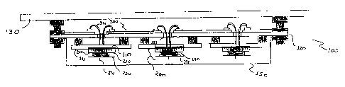
The novel antenna system comprises an antenna
assembly as shown generally at 100 in Figure 1. The
assembly 100 comprises a plurality (preferably 3) of
circular metallic disks 110, preferably deposed upon an
antenna PCB substrate 111, each of which holds a
plurality (preferably 6) of directional beam antennas
210, which in the preferred embodiment each comprise a
double-sided printed circuit monopole Yagi-Uda antenna
vertically oriented around the disk 110 circumference and
connected by an SMA conductor 220 soldered therewith, as
shown in Figures 2 and 3. Preferably, each circular
metallic disk 110 is deposited upon the antenna PCB
substrate 111 and has a 24 cm diameter. The centre
conductor 220 of the Yagi-Uda antenna 210 is soldered to
its driver 213, while the reflector 212 and directors
214, 215 are soldered to ground.
The disks 110 are suspended below a planar
board 120 having holes 121 cut therein co-axial with the
centre of each disk 110. Preferably, the planar board
120 is comprised of Perspex (TM) material. The holes 121
permit electrical connection by way of cables 901 to pass
from the antenna components mounted on one side thereof
to the control circuitry 900 mounted on the other side.
Because of the large number of identical Yagi-
Uda antennas 210 that make up the inventive antenna
system (in the preferred embodiment 18),
manufacturability and reproducibility concerns are
addressed by printing the monopoles 210 on a monopole
-6-
CA 02565032 2006-10-20
19207P0022CA01
dielectric substrate 211 that is vertically mounted in
spoke-like fashion around each horizontal disk 110.
The inventive use of double-sided PCB
manufacturing technology permits more accurate monopole
heights that correspond to more accurate beam shapes and
design flexibility, while maintaining stability, good
gain, wide bandwidth and low return loss characteristics.
Simulations have shown that performance is also generally
improved over discrete wire monopole Yagi-Uda antennas.
Each Yagi-Uda antenna 210 has one reflector
212, one driver 213 and two director elements 214, 215
and is made by etching identical strips on both sides of
the PCB dielectric substrate 211. The double-sided
pattern of such an antenna provides both symmetrical
pattern and a higher radiation efficiency over prior
attempts to mass produce Yagi-Uda antennas using single
sided PCB techniques.
Preferably, the monopole dielectric substrate
211 is thin, of approximately 0.787 mm, to avoid
dielectric losses, and manufactured from FR4 material
having a permittivity of 4.2 and a tangent loss of 0.02.
In a preferred embodiment, each monopole
dielectric substrate has a length of 8 cm and a width of
3 cm. To achieve operation in the 2.43 GHz, band as
shown in Figure 3, the reflector 212 is preferably 27.5
mm long, the driver 213 is 24.6 mm long, the first
director 214 is 21.7 mm long and the second director 215
is 22.4 mm long. The reflector 212 and driver 213 are
-7-
CA 02565032 2006-10-20
19207P0022CA01
separated by 25.5 mm, while the driver 213 and first 214
and second directors 215 are each separated by 21.2 mm.
Each strip is 2 mm wide and the distal ends of each strip
are connected through the substrate by vias 218. An SMA
conductor 219 is connected to the driver 213 and adapted
to conductively engage the SMA conductor 220 on the disk
110.
The positioning of the directional beam antenna
210 about the disk 110 is an important factor for
determining the performance of the inventive MIMO antenna
sub-assembly shown generally in Figure 1. Preferably,
the near edge of each antenna substrate is positioned 25
mm from the centre of the disk 110. This can be
facilitated by a cylindrical horizontal spacer hub 140
mounted coaxially with the centre of the disk 110 as
shown in Figure 1. The horizontal spacer hub 140 is not
shown on Figure 2 for clarity purposes only.
Simulations have shown that the double sided
PCB monopole Yagi-Uda antenna 210 has high efficiency and
a beam pattern that is symmetrical due to the double
sided etching. The input reflection is well below -10dB
through a bandwidth of 150 MHz without any extra matching
circuits.
The monopole implementation has the advantage
of being of shorter length compared to a dipole Yagi-Uda
antenna and an easier feed with good matching. In the
preferred embodiment, the Yagi-Uda monopole antenna 210
has a height of almost a quarter wavelength, that is half
-8-
CA 02565032 2006-10-20
19207P0022CA01
of the height of conventional printed circuit Yagi-Uda
dipole antennas and thus boasts a low profile.
Each of these directional beam antennas 210
generate a beam with an azimuth beamwidth so that
together, the antennas 210 co-located on a disk 110
generate a 360 coverage pattern.
A sectorized sleeve monopole antenna 231, which
is preferably an omni-directional antenna, is co-located
coaxially with each disk 110 on a small ground plane 230
above the directional beam antennas 210 as shown on
Figure 1.
Any desired vertical spacing between the ground
plane 230 and the directional beam antennas 210 may be
provided by a second cylindrical vertical spacer hub 141
positioned coaxially with and abutting against the
horizontal spacer hub 140. Preferably, the vertical
spacer hub 141 is of larger diameter than the horizontal
spacer hub 140, as shown in Figure 1, to provide a more
stable base for the ground plane 230. However, those
having ordinary skill in this art will readily appreciate
that a single hub of appropriate dimension could replace
both the horizontal 140 and vertical 141 spacer hubs.
Each disk 110, together with the vertical
directional beam antennas 210 and the omni-directional
antenna 231 comprise a single MIMO antenna sub-assembly
200.
Each MIMO antenna sub-assembly 200 is separated
from its neighbour, in order that it intercepts an
-9-
CA 02565032 2006-10-20
19207P0022CA01
independent data stream from a wireless subscriber. The
throughput is thus additively enhanced when compared to
single antenna systems such as that covered by the
802.11a, 802.11b and 802.11g standards.
Preferably, the MIMO antenna sub-assemblies 200
are positioned in a linear array to minimize mutual
shadowing. Simulations suggest that the antenna assembly
100 is preferably mounted on a ceiling 130 similar to a
fluorescent tube light fixture.as shown in Figure 1. In
order to protect the sensitive antenna elements, the
antenna assembly 100 is preferably enclosed by a radome
150.
Figure 4 shows the measurement setup used to
generate certain simulation and measurement results
relating to the MIMO sub-assembly 200.
Figure 5 shows a three-dimensional simulated
pattern at 2.4 GHz derived using ANSOFT Corporation HFSS.
The pattern shown is for the inventive MIMO sub-assembly
200 at an elevation angle of 75 and an omni-directional
monopole antenna operating at a frequency of 2.5 GHz.
Figure 6 shows a measured antenna beam pattern
for the MIMO sub-assembly 200.
Figure 7 shows an overlay of simulation results
of an omni-directional monopole antenna operating at a
frequency of 2.5 GHz and the MIMO sub-assembly at an
elevation angle of 75 .
-10-
CA 02565032 2006-10-20
19207P0022CA01
Figure 8 shows an additional overlay of a
simulation result of the MIMO sub-assembly at an
elevation angle of 90 .
Figure 9 is a block diagram of processing
components, shown generally at 900 in Figure 9. The
processing components 900 are connected to the omni-
directional antenna 231, the plurality of directional
beam antennas 210 and an 802.11n compliant processor 970
and comprise a beam selector switch 905, a plurality of
pre-selector filters 910, 915, a plurality of RF transmit
/ receive converters 920, 925, a plurality of power
amplifiers for transmission 921, 926, a line switch 930,
a processor assembly 940, a beam transmit / receive
switch 950, an omni transmit / receive switch 955, a
receive omni / beam switch 960 and a transmit omni / beam
switch 965.
The beam selector switch 905 is connected to
each of the directional beam antennas 210 corresponding
to a single MIMO antenna sub-assembly 200 via cables 901
and to the pre-selector filter 910. It provides
electrical RF connection between the selected antenna
from the directional beam antennas 210, each of which
corresponds to a beam, and the pre-selector filter 910.
Typically, the switching time for the beam selector
switch 905 is on the order of 150 ns.
There is a pre-selector filter 910 associated
with the selected directional beam antennas 210 and a
pre-selector filter 915 associated with the omni-
directional antenna 231. The pre-selector filter 910 is
-11-
CA 02565032 2006-10-20
19207P0022CA01
connected to the output of the beam selection switch 905
and the RF transmit / receive converter 920. The pre-
selector filter 915 is connected between the omni-
directional antenna 231 via cables 901 and the RF
transmit / receive converter 925. The pre-selector
filters 910, 915 condition the signal
received/transmitted along its associated antenna.
The RF transmit / receive converter 920 is
connected to the pre-selector filter 910, to the line
switch 930 and receives control signals 947 from the
processor assembly 940. The RF transmit / receive
converter 925 is connected to the pre-selector filter
915, to the omni transmit / receive switch 955 and
receives control signals 946 from the processor assembly
940. The RF transmit / receive converters 920, 925
convert signals received from its associated pre-selector
filter 910, 915 from RF down to baseband I & Q signals
and I & Q signals received for transmission to its
associated pre-selector filter 910, 915 from baseband up
to RF. Preferably, the RF transmit / receive converters
920, 925 are MAX 2829 IC chips with an internal low noise
amplifier and paired with an associated power amplifier
PA model number MAX 2247 and has a noise figure [NF] of
3.5 dB. Those having ordinary skill in this art will
readily appreciate that if the RF transmit / receive
converters 920, 925 do not have internal low noise
amplifiers, a discrete amplifier may be connected
therewith as appropriate.
-12-
CA 02565032 2006-10-20
19207P0022CA01
The line switch 930 is connected to the RF
transmit / receive converter 920, the processor assembly
940 and the beam transmit / receive switch 950 and
receives control signals 943 from the processor assembly
940. It tests the various beams and passes baseband I &
Q signals received from the various Yagi-Uda antennas 210
through the pre-selector filter 910 and the RF transmit /
receive converter 920 to the processor assembly 940, in
order to identify the best beam to be used for a SS, and
an operational mode in which baseband I & Q signals
directed to and emanating from the identified best beam
along the RF transmit / receive converter 920 are passed
from and to the beam transmit / receive switch 950.
The processing assembly 940 is connected to the
line switch 930. It receives control signals 971, 972
from the 802.11n compliant processor 970 and issues
control signals 947, 946, 943, 944, 945 to the RF
transmit / receive converters 920, 925, to the line
switch 930, to the beam transmit / receive switch 950, to
the omni transmit / receive switch 955 respectively.
Preferably the processing assembly 940 comprises an
analog to digital conversion subsystem 941 and a
processing subsystem 942. In a preferred embodiment, the
processing assembly is implemented in an field-
programmable gate array (FPGA). An exemplary logical
block diagram of the FPGA is shown in Figure 10.
The analog to digital conversion subsystem 941
converts baseband I & Q signals received from the line
switch 930 while in best beam selection mode to digital
-13-
CA 02565032 2006-10-20
19207P0022CA01
form and forwards the digital information to the
processing sub-system 942, where the information is
evaluated and a best beam selected for the SS in
question.
The processing subsystem 942 also receives
signals from the 802.11n compliant processor 970 in the
form of commands to move from an omni-directional mode to
a beam mode and vice versa 971, and to move from a
transmit to a receive mode and vice versa 972. The
processing subsystem 942 thereafter generates control
signals to the various switches and RF transmit / receive
converters to give effect to the commands received from
the 802.11n compliant processor 970.
The beam transmit / receive switch 950 is
connected to the line switch 930, to the receive omni /
beam switch 960, to the transmit omni / beam switch 965
and receives control signals 944 from the processing
assembly 940. The beam transmit / receive switch 950
moves, in response to control signals 944 from the
processing assembly 940, between a transmit mode in which
it passes information from the transmit omni / beam
switch 965 to the line switch 930 and a receive mode in
which it passes information from the line switch 930 to
the receive omni / beam switch 960.
The receive omni / beam switch 960 is connected
to the beam transmit / receive switch 950, the omni
transmit / receive switch 955 and the 802.11n compliant
processor 970. The receive omni / beam switch 960 moves
in response to control signals from the processing
-14-
CA 02565032 2006-10-20
19207P0022CA01
assembly 940 between an omni mode in which signals
originally received at the omnidirectional antenna 231
are passed by the omni transmit / receive switch 955 to
the 802.11n compliant processor 970 and a beam mode in
which signals originally received at a designated best
beam corresponding to one of the directional beam
antennas 210 are passed on by the beam transmit / receive
switch 950 to the 802.11n compliant processor 970.
The transmit omni / beam switch 965 is
connected to the 802.11n compliant processor 970, the
beam transmit / receive switch 950 and the omni transmit
/ receive switch 955. The transmit omni / beam switch 970
moves in response to control signals from the processing
assembly between an omni mode in which signals generated
by the 802.11n compliant processor 970 are passed to the
omni transmit / receive switch 955 for transmission by
the omnidirectional antenna 231 and a beam mode in which
signals generated by the 802.11n compliant processor 970
are passed to the beam transmit / receive switch 950 for
transmission to the designated best beam corresponding to
one of the directional beam antennas 210.
The 802.11n compliant processor 970 is
connected to the receive omni / beam switch 960, the
transmit omni / beam switch 965 and generates commands to
the processing assembly 940 including to switch between a
transmit mode and a receive mode 972. It is anticipated
that third party manufacturers will design and implement
such processors to provide Wi-Fi functionality in
accordance with the evolving 802.11n standard. In most
-15-
CA 02565032 2006-10-20
19207P0022CA01
of these cases, such processors will be expecting that
each of the MIMO antennas will be a sectorized antenna
such as the omnidirectional antenna 231, rather than a
plurality of directional beam antennas 210. In such a
scenario, some additional logic to permit the 802.11n
compliant processor 970 to generate commands to the
processing assembly 940 to switch between an omni mode
and a beam mode 971 may be appropriate.
Where, as in the preferred embodiment, the
antenna assembly 100 comprises a plurality of MIMO
antenna sub-assemblies 200, each of the MIMO antenna sub-
assemblies will interface with a common 802.11n compliant
processor 970, where the combining of the signals from
each of the MIMO antennas takes place, to increase
throughput and SINR.
In operation, when a SS is detected, preferably
by receipt of an RTS signal along the omnidirectional
antenna 231, the received antenna signal is filtered by
the pre-selector filter 915, attenuated and/or amplified
as required for noise minimization purposes and down-
converted to a series of baseband I & Q signals by
receiver circuitry on the RF transmit / receive converter
925 and fed to the the omni transmit / receive switch
955, which is initially in receive mode.
The signal is fed out of the omni transmit /
receive switch 955 and into the receive omni / beam
switch 960, which is initially in omni mode.
-16-
CA 02565032 2006-10-20
19207P0022CA01
The signal is fed out of the receive omni /
beam switch 960 and into the 802.11n compliant processor
970, where it is processed in conventional fashion.
Additionally, the 802.11n compliant processor 970
identifies an opportunity to identify a best beam for the
communications between the AP with which the antenna
assembly 100 is associated and the SS in question. It
initiates this task by notifying the processor assembly
940, along control signal 971, to move from an omni mode
to a beam mode.
In consequence thereof, if necessary, the
processor assembly 940 issues control signal 947 to the
RF transmit / receive converter 920, activating it and
sending it into receive mode, control signal 943 to the
line switch 930, sending it into best beam calculation
mode, control signal 944 to the beam transmit / receive
switch 950, sending it into receive mode.
As a result, antenna signals received at the
various directional beam antennas 210 will be
successively switched by beam selector switch 905 into
connection with the pre-selector filter 910 where it is
filtered and then attenuated and/or amplified as required
for noise minimization purposes and down-converted to a
series of baseband I & Q signals by receiver circuitry on
the RF transmit / receive converter 920 and fed to the
line switch 930, which is in best beam selection mode.
The signal received at each of the directional beam
antennas 210 is received as baseband I & Q signals by the
analog to digital conversion subsystem 941, converted
-17-
CA 02565032 2006-10-20
19207P0022CA01
into digital format and fed to the processing subsystem
942 where it is processed. From a comparison of the
digitized antenna signals, the processing subsystem 942
identifies the best beam for the SS in question.
Thereafter, processing assembly 940 issues
control signal 943 to the line switch 930 to send it into
operational mode and the 802.11n compliant processor 970
will thereafter use the identified best beam for all
communications with the SS, until superseded by a
subsequent best beam or the best beam is declared non-
functioning.
For signals received from the SS while in the
beam operational mode, antenna signals received at the
directional beam antenna 210 identified with the best
beam will be switched by beam selector switch 905, which
is activated by a control signal from the processing
assembly 940, into connection with the pre-selector
filter 910 where it is filtered and then attenuated
and/or amplified as required for noise minimization
purposes and down-converted to a series of baseband I & Q
signals by receiver circuitry on the RF transmit /
receive converter 920 and fed to the line switch 930,
which is in operational mode. As a result, the signal
received at the directional beam antenna 210 is passed as
baseband I & Q signals through the beam transmit /
receive switch 950, which, if necessary, will have been
sent into receive mode by the processing assembly 940
along control signal 944, through the received omni /
beam switch 960, which, if necessary, will have been sent
-18-
CA 02565032 2006-10-20
19207P0022CA01
into beam mode by the processing assembly 940 along
control signal 944 and to the 802.11n compliant processor
970 for processing in conventional fashion.
Those having ordinary skill in this art will
readily recognize that the processing involved in
determining the best beam will require some time and that
in the interim, there may be incoming signals from the
SS. In such an eventuality, the signals are received by
the omnidirectional antenna 231 and processed in the same
manner as the initial RTS signal. This permits the
antenna assembly 100 the luxury of not having to identify
the best beam within any minimum time period.
Additionally, there may be occasions when the
directional beam antennas 210 are not available or the
best beam estimate may be considered no longer current,
such as because of movement of the SS. In such
situations, the antenna assembly 100 may revert to using
the omnidirectional antenna 231.
During the course of processing, the 802.11n
compliant processor 970 may identify some signal that
needs to be communicated to the SS. If there is no best
beam identified for communications with the SS, the
802.11n compliant processor 970 signals the processing
assembly 940 along control signal 972 to move to a
transmit mode.
This in turn prompts the processing assembly
942, if necessary, to issue control signal 946 to the RF
transmit / receive converter 925 sending it into transmit
-19-
CA 02565032 2006-10-20
19207P0022CA01
mode, control signal 945 to the omni transmit / receive
switch 955 sending it into transmit mode, and control
signal to the transmit/omni beam switch 965 sending it
into omni mode.
As a result, signals from the 802.11n compliant
processor 970 are sent to the transmit omni / beam switch
965, to the omni transmit / receive switch 955 and to the
RF transmit / receive converter 925, where they are
converted from baseband I & Q signals into RF signals,
conditioned as necessary, sent to the pre-selector filter
915 to be filtered and transmitted to the SS along the
omnidirectional antenna 231.
On the other hand, if there is a best beam
identified for the SS, the 802.11n compliant processor
970 signals the processing assembly 940 along control
signal 972 to move to a transmit mode and, if necessary,
along control signal 971 to move to a beam mode.
This in turn prompts the processing assembly
942, if necessary, to issue control signal 947 to the RF
transmit / receive converter 920 sending it into transmit
mode, control signal 943 to the line switch 930 to send
it into operational mode, control signal 944 to the beam
transmit / receive switch 955 sending it into transmit
mode.
As a result, signals from the 802.11n compliant
processor 970 are sent to the transmit omni / beam switch
965, to the beam transmit / receive switch 950, to the
line switch 930 and to the RF transmit / receive
-20-
CA 02565032 2006-10-20
19207P0022CA01
converter 920, where they are converted from baseband I &
Q signals into RF signals, conditioned as necessary, sent
to the pre-selector filter 910 to be filtered, through
the beam selector switch 905, which is configured to
connect it to the directional beam antenna 210 associated
with the designated best beam, for transmission to the
SS.
In addition to the time interval during which
the processing assembly 940 is attempting to determine
which of the directional beam antennas 210 is to be
designated as providing the best beam, there are two
other occasions when the antenna system 100 may enter the
omni mode, namely in the case of hidden nodes, or where
there is a desire on the part of the user to transmit
omni.
Turning now to Figure 10, there is shown a flow
chart showing the processing steps involved in
determining the best beam for an SS.
Initially, one of the plurality (in the
preferred embodiment, 6) of directional beam antennas 210
is selected 1010 using the beam selector switch 905. The
received antenna signal is processed by an edge-detection
module 1020 in order to identify the start of the packet.
Once the start of the packet has been
identified, the process of calculating covariance
matrices 1030 is commenced. The performance of each beam
is identified by measuring the coefficients of the
channel defined between the multiple antennas of the SS
-21-
CA 02565032 2006-10-20
19207P0022CA01
and the multiple antennas of the antenna system 100 of
the AP. The coefficients define the effective impedance
of the channel, in terms of the phase shift and
attenuation of the signal encountered by the channel.
From the computed covariance matrices, the
maximum and minimum eigenvalues are determined by eigen
decomposition 1040.
With this information, the condition number for
the selected beam may be determined 1050. The condition
number is calculated as the ratio of the largest
eigenvalue over the smallest eigenvalue.
This process is repeated for each of the
potential best beams 1060, by returning 1062 to the
select beam step 1010 if not all of the beams have been
selected and proceeding to the next step 1061 only when
all of the beams have been selected and condition numbers
identified for each beam.
Once all of the condition numbers have been
identified, the beam corresponding to the best condition
number is stored in a look-up table entry corresponding
to the SS 1070. In addition to the best beam number (and
optionally the condition number), the MAC address for the
SS is also stored so that the best beam associated with
that SS can be later retrieved.
Those having ordinary skill in this art will
readily recognize that while the processing just
described contemplates the choice of the best beam from
among the plurality of directional beam antennas 210 in a
-22-
CA 02565032 2006-10-20
19207P0022CA01
single multi-beam assembly 200, it is certainly feasible
to consider selecting the best beam for each of the MIMO
antenna sub-assemblies 200 from among all of the
directional beam antennas 210 in order to maximize the
performance of the antenna system 100 overall, and not on
a MIMO antenna sub-assembly 200 basis only. Thus, in the
exemplary embodiment of a linear array of three MIMO
antenna sub-assemblies 200 each comprising six
directional beam antennas 210, three best beams could be
designated, each associated with one of the MIMO antenna
sub-assembly 200, but based on the overall performance
provided across all eighteen directional beam antennas
210 in the antenna assembly 100.
After all the beams are selected, the best beam
number and MAC address are stored in the look-up table.
At this point, the processing determines if the
next general interval has been reached 1080. The general
interval is a time interval chosen to represent a
convenient point at which the best beam information can
be used to switch from omni mode to beam mode. If the
general interval has not been reached 1082, the beam
selection process is repeated. If, however, the general
interval has been reached 1081, the best beam information
stored in the look-up table is handed over.
After the best beam information has been handed
over, the processing checks to see if a predetermined
time interval (in the preferred embodiment 10 ms) has
expired. The time interval represents the repeat
frequency of checking for the best beam. If the time
- 23 -
CA 02565032 2006-10-20
19207P0022CA01
interval has not expired, the processing loops back
around 1102. If the time interval has expired 1101, the
beam selection process is repeated.
The present invention can be implemented in
digital electronic circuitry, or in computer hardware,
firmware, software, or in combination thereof. Apparatus
of the invention can be implemented in a computer program
product tangibly embodied in a machine-readable storage
device for execution by a programmable processor; and
methods actions can be performed by a programmable
processor executing a program of instructions to perform
functions of the invention by operating on input data and
generating output. The invention can be implemented
advantageously in one or more computer programs that are
executable on a programmable system including at least
one input device, and at least one output device. Each
computer program can be implemented in a high-level
procedural or object oriented programming language, or in
assembly or machine language if desired; and in any case,
the language can be a compiled or interpreted language.
Suitable processors include, by way of example,
both general and specific microprocessors. Generally, a
processor will receive instructions and data from a read-
only memory and/or a random access memory. Generally, a
computer will include one or more mass storage devices
for storing data files; such devices include magnetic
disks, such as internal hard disks and removable disks;
magneto-optical disks; and optical disks. Storage
devices suitable for tangibly embodying computer program
-24-
CA 02565032 2006-10-20
19207P0022CA01
instructions and data include all forms of volatile and
non-volatile memory, including by way of example
semiconductor memory devices, such as EPROM, EEPROM, and
flash memory devices; magnetic disks such as internal
hard disks and removable disks; magneto-optical disks;
CD-ROM disks; and buffer circuits such as latches and/or
flip flops. Any of the foregoing can be supplemented by,
or incorporated in ASICs (application-specific integrated
circuits), FPGAs (field-programmable gate arrays) or DSPs
(digital signal processors).
Examples of such types of computers are the
processing sub-assembly 942 and the 802.11n compliant
processor 970 contained in antenna assembly 100, suitable
for implementing or performing the apparatus or methods
of the invention. The system may comprise a processor, a
random access memory, a hard drive controller, and an
input/output controller coupled by a processor bus.
It will be apparent to those skilled in this
art that various modifications and variations may be made
to the embodiments disclosed herein, consistent with the
present invention, without departing from the spirit and
scope of the present invention.
Other embodiments consistent with the present
invention will become apparent from consideration of the
specification and the practice of the invention disclosed
therein.
Accordingly, the specification and the
embodiments are to be considered exemplary only, with a
-25-
CA 02565032 2006-10-20
19207P0022CA01
true scope and spirit of the invention being disclosed by
the following claims.
-26-