Note : Les descriptions sont présentées dans la langue officielle dans laquelle elles ont été soumises.
CA 02565288 2006-11-01
WO 2005/122354 PCT/F12005/000267
1
ISOLATED MEASUREMENT CIRCUIT FOR SENSOR RESISTANCE
BACKGROUND OF THE INVENTION
The invention relates to measuring the resistance of a resistive
sensor, such as a PTC or NTC thermistor sensor used for monitoring the
temperature of electrical machines, particularly the windings of a squirrel
cage
motor.
In addition to protection of a squirrel cage motor based on current
measurement, thermistor sensors can be used to protect windings against
overheating, for example when the ambient temperature rises or motor cooling
is insufficient for any reason. When a squirrel cage motor is used in an
explosive atmosphere (Exe), the regulations require that the motor must be
equipped with a temperature measurement circuit and the measurement
circuit of the thermistor sensor must be galvanically isolated from the other
electronic circuits of the system. In practical three-phase motors, three
thermistor sensors are connected in series, one for the stator winding of each
phase.
The invention makes it possible to measure sensor resistance over
a wide resistance range, which enables the use of different types of sensors
while still providing a reliable indication of a short circuit or break in the
sensor
circuit. The invention can also be used in situations where high voltage
strength (insulation level) is required between the sensor circuit and SELV
electronics.
One prior art solution is based on AC technology, including an
astable multivibrator operating on a selected frequency and a galvanic
connection between the measurement circuit and the device electronics.
Galvanic isolation is implemented by means of an isolation transformer
between the thermistor sensor and measurement circuit. A disadvantage of
this solution is the non-linearity of the isolation transformer and its poor
response, particularly at low sensor resistance values, which makes it
difficult
to indicate a short circuit. Another disadvantage is the effect of capacitance
in
CONFIRMATION COPY
CA 02565288 2006-11-01
WO 2005/122354 PCT/F12005/000267
2
the sensor circuit conductors, which is summed to the measurement circuit
through the isolation transformer in addition to the actual effect of the
sensor
resistance. Galvanic isolation by an isolation transformer is simple to
implement, and the solution is inexpensive.
Another prior art solution is the use of a linear opto-isolator, but this
causes problems due to the high price of the component and large differences
in tolerance between the individual components, which makes the
implementation of calibration for the measurement circuit complicated.
Reliability and stability in long-term use are poor as well. The advantage of
this
solution is good linearity over a wide range of resistance and a rapid
operating
response.
An electric motor manufacturer most typically chooses a PTC
thermistor sensor, the resistance of which changes very sharply just below the
maximum temperature allowed for the winding insulation. A prior art solution
based on this compares the resistance value of the thermistor sensor with a
fixed threshold value. Crossover of the threshold value is indicated either by
a
change in the current load of the isolation transformer or by an opto-
isolator.
The solution is very inexpensive, but its disadvantage is the ON/OFF type
status information; no information is available on the state of change in the
resistance value ¨ for example, whether it is approaching the threshold value
slowly or rapidly. No indication of a short circuit fault in the sensor
circuit is
provided either.
There is also an integrated circuit in the market, Maxim Max 6691,
that allows the connection of four PTC or NTC sensors. The chip converts the
resistance value of each sensor to one Pulse Width Modulated (PWM) pulse;
however, the range of the pulse ratio is quite narrow. The PWM pulse ratio
decreases with increasing resistance, so the chip is most easily applicable to
a
NTC sensor. The linear operation of the circuit makes it difficult to
distinguish a
short circuit from small values of resistance. The measurement range can be
adjusted using a resistance connected in series with the sensor, but the
usable measurement range in each case is too restricted with regard to an
application for measuring the temperature of electric motor windings and
CA 02565288 2012-06-27
3
protecting them. There is no second-source manufacturer of the chip, which
means that it will bind the user to a single component supplier.
There is another integrated circuit, Smartec SMT 160-30, with an
internal temperature sensor and PWM output. Due to its physical size and
limited operating temperature range, the chip is not applicable to the
protection
of electric motor windings. The PWM frequency of the chip output is 1...4 kHz,
which also Sets excessively tight requirements for the interface component and
the circuits for analysing the measurement result.
SHORT DESCRIPTION OF THE INVENTION
A purpose of the invention is to create a measurement circuit for a
resistive sensor that would solve the problems referred to above.
According to an aspect of the present invention there is provided a
sensor resistance measurement circuit comprising:
a sensor connection that connects a resistive sensor to a voltage
divider circuit, means for supplying voltage (UD) to said voltage divider
circuit,
said means for supplying voltage comprising a non-inverting amplifier stage
for amplifying the sensor signal and a differential amplifier stage which,
based on the difference between the amplified sensor signal connected to its
inverting input and a regulated reference voltage connected to its non-
inverting input, is arranged to supply the voltage divider circuit, said
voltage
divider circuit comprising:
a resistance in series, and
means for filtering the voltage over a sensor resistance into a sensor
signal, and means for processing and further transmitting the sensor signal,
wherein the means for supplying voltage to the voltage divider circuit have
been arranged to continuously reduce the supplied voltage as a function of
the sensor resistance.
In some embodiments the means for processing and further
transmitting the sensor signal comprises:
means for amplifying the sensor signal into a signal voltage,
a sawtooth generator,
CA 02565288 2012-06-28
3a
a comparator for generating a pulse-encoded PWM signal as a result
of a comparison between the signal voltage and the output voltage of said
sawtooth generator, and
means for further transmitting said PWM signal.
According to another aspect of the present invention there is provided
a method for measuring sensor resistance, the method comprising:
supplying a voltage to a voltage divider circuit and, processing said
sensor signal for further transmission,
wherein the voltage supplied to the voltage divider circuit is
continuously reduced as a substantially logarithmic function of the sensor
resistance.
In some embodiments the method further comprises:
amplifying the sensor signal into a signal voltage, and comparing the
signal voltage with a sawtooth wave in order to generate a pulse-encoded
PWM signal for further transmission.
According to a further aspect of the present invention there is provided
a resistance measurement circuit that measures a resistance of a first
resistive element, the circuit comprising:
a voltage divider circuit having a connector that receives the first
resistive element, said voltage divider circuit comprising:
a second resistive element that is connected in series with the
first resistive element, and
a filter that filters the voltage over the first resistive element into
a signal;
a voltage supply that supplies voltage to said voltage divider
circuit; and
a first circuit that processes and further transmits the signal;
wherein the voltage supply reduces the supplied voltage as a
function of the resistance of the first resistive element; and
wherein the supplied voltage is continuously reduced as a
substantially logarithmic function of the resistance of the first resistive
element.
CA 02565288 2012-06-27
3b
In some embodiments the voltage supply comprises:
a non-inverting amplifier stage that amplifies the signal; and
a differential amplifier stage which, on the basis of the difference
between the amplified signal connected to its inverting input and a regulated
reference voltage connected to its non-inverting input, supplies a voltage to
the voltage divider circuit.
In some embodiments the first circuit comprises:
an amplification circuit that amplifies the signal into a signal voltage;
a sawtooth generator;
a comparator that generates a pulse-encoded PWM signal as a result
of a comparison between the signal voltage and the output voltage of said
sawtooth generator; and a second circuit configured to further transmit said
PWM signal.
In addition to sensor resistance measurement, the invention also
indicates a short circuit or break in the sensor circuit.
The invention is based on an electronic circuit in which conductors
from a resistive sensor located in the object to be protected ¨ typically an
WC
or PTC temperature sensor ¨ are connected to an amplifier circuit in a
feedback configuration within the voltage divider circuit. The amplffier
reduces
the DC level supplied to the voltage divider when the sensor resistance
increases. The signal is amplified, and a continuous Pulse Width Modulation
signal is generated using a sawtooth generator and comparator. The signal is
transmitted to a SELV electronic circuit in digital format through an opto-
isolator.
The frequency of the sawtooth, generator can be low, because the
time constants of the object of measurement, which are in the order of more
than one second, allow for a long response time for the measurement result.
This makes it possible to use inexpensive opto-isolators. In order to manage
resolution over a wide range of resistance measurement (50 ... 15 kr/), the
Intention is to imitate logarithmic response with an amplifier circuit that is
as
CA 02565288 2006-11-01
WO 2005/122354 PCT/F12005/000267
4
simple as possible. The more the voltage over the sensor increases, the more
the amplifier reduces the voltage supplied to the voltage divider circuit.
This
means that a better resolution is achieved at lower resistance values, which
facilitates the indication of a short circuit in the sensor circuit.
The isolation of a digital signal using an opto-isolator is a better
method than the isolation of an analogue signal using a linear opto-isolator
with poorer long-term stability.
The resolution required for the protection of an electric motor is
typically 7.5%, which means that coarse resolution is enough for the
measurement circuit, but the temperature range for measurement is wide,
typically extending to temperatures in excess of 150 C.
The arrangement according to the invention allows a wide
measurement range, in practice 50 û ... 15 kg), and is most sensitive in the 1
kS2 ... 5 IcS2 range, which covers the threshold levels of the most common PTC
or NTC thermistors. The feedback block used in the solution according to the
invention makes it possible to achieve sufficient selectivity for the
detection of
fault situations ¨ including a short circuit as well as an open circuit. The
invention makes it possible to achieve a lower price and easier calibration
compared with solutions implemented using a linear opto-isolator. Calibration
can be carried out reliably using no more than two measurement points.
Another advantage of the invention is that due to the supply voltage feedback
block used, the voltage over the sensor resistance is very low, less than 2 V,
and it is preferably supplied to the sensor through a series resistor in the
order
of 20 K2. This means that it is very safe to locate the thermistor sensor
connected to the circuit within an explosive Ex atmosphere because it remains
clearly below the critical levels for electric sparking. The low-frequency PWM
technology used in the invention also enables the use of slightly slower opto-
isolators with a high isolation voltage strength. The reliability of opto-
isolator
operation in long-term use is crucial, so the opto-isolator must be selected
from sufficiently high-quality components proportioned to the application.
Instead of PWM (Pulse Width Modulation), some other encoding
method can be used for encoding the sensor signal into a digital format.
CA 02565288 2006-11-01
WO 2005/122354 PCT/F12005/000267
SHORT DESCRIPTION OF THE FIGURES
In the following, the invention will be described in more detail
through example embodiments and references to the enclosed drawings,
5 where
Figure 1 illustrates the measurement arrangement as a block
diagram;
Figure 2 illustrates the circuit diagram of blocks C, D and E;
Figure 3 illustrates the circuit diagram of block F;
Figure 4 illustrates the circuit diagram of blocks G and H;
Figure 5 is a graph of the PWM pulse ratio [%] as a function of
sensor resistance.
DETAILED DESCRIPTION OF THE INVENTION
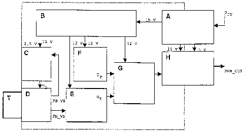
Figure 1 illustrates the sensor measurement electronic circuit as a
block diagram. The dotted line limits the area of isolated measurement
electronics, with a SELV electronic circuit on the outside.
Block A preferably comprises a secondary winding of triple-
insulated wire added to the ferrite transformer in a DC/DC switching-mode
power supply that is already included in the measurement device. This
provides the isolated measurement electronics with the required electric
power, typically 15 V, 10 mA. Other power supply configurations with the
required insulating strength can also be used.
Block B includes means for generating a regulated DC voltage,
such as 12 V, for supplying the measurement electronics; preferably, this is a
shunt regulator with associated components.
Block C comprises an amplifier stage in a feedback configuration
that supplies a DC voltage (UD) to the sensor circuit so that when sensor
resistance (Rx) increases, the supplied voltage level decreases in order to
create a function that imitates logarithmic response.
CA 02565288 2006-11-01
WO 2005/122354 PCT/F12005/000267
6
Block D comprises a voltage divider circuit consisting of a ballast
resistor in series with the sensor resistance to be measured. Furthermore, the
block includes components associated with EMC filtering and over-voltage
protection fulfilling the requirements for Ex circuits.
Block T comprises the measurement sensor connectors.
Block E comprises a non-inverting amplifier stage that amplifies the
voltage (Ux) over the sensor resistance in the voltage divider circuit.
Preferably, the amplifier gain is in the order of 8.
Block F comprises a sawtooth generator for generating a PWM
signal. The generator frequency is preferably in the order of 10 ... 100 Hz.
When protecting an electric motor, a time constant that is in the order of
more
than one second makes it possible to advantageously use a frequency of 40
Hz, for example. The amplitude of the sawtooth wave (UF) is dimensioned to
the 10 V level, for example ¨ that is, somewhat lower than the supply voltage
level chosen for the electronics, such as 12 V.
Block G comprises a comparator circuit that compares the amplified
sensor voltage signal (UE) and the output voltage (UF) of the sawtooth
generator, generating a PWM signal and driving the opto-isolator in block H.
In
addition to the opto-isolator, block H comprises a series resistance connected
to the positive supply voltage, as well as means for keeping the pulse edge
sufficiently sharp on the secondary side. The PWM output signal is transmitted
from the isolated measurement electronic circuit through the opto-isolator to
the main electronic circuit.
In order to manage the resolution of resistance measurement over
a wide measurement range (50 Q ... 15 Id2), the intention of the amplifier
circuit in block C is to imitate logarithmic response using the simplest
possible
method. At low values of thermistor resistance the output voltage ¨ that is,
the
PWM ratio ¨ increases proportionally more rapidly than at high resistance
values. This makes it easier to distinguish a short circuit from the minimum
values of the thermistor sensor. The operation of the feedback block C plays a
crucial role in this. The more the voltage (Ux) over the sensor increases, the
more block C reduces the voltage (UD) supplied to the voltage divider circuit.
Provided that a 201(0 ballast resistor is connected in series with the
thermistor
CA 02565288 2006-11-01
WO 2005/122354 PCT/F12005/000267
7
resistance Rx, the voltage supplied by block C to the voltage divider circuit
can
be stated as:
UD =10 V -6=Ux (1)
so, when observing the 8-fold gain of block E and the 0...10 V
amplitude range of the sawtooth generator (block F), the cycle ratio (nom ) of
the outgoing PWM signal is:
8. R.,
17OUT = (2)
7. Rx + 20 k5-2
Figure 2 illustrates the circuit diagram of the thermistor sensor
interface circuit (block D), the feedback amplifier stage (block C) and the
amplifier stage (block E).
The operational amplifier (A501-B) in the feedback amplifier stage
(block C) together with the resistances (R515, R524) forms a non-inverting
amplifier stage with a preferred gain ratio of two. The operational amplifier
(A501-C) together with the resistances (R510, R514) and a regulated
reference voltage Uref connected to the positive (+) input, for example +2.5
V,
forms a differential amplifier with a preferred gain ratio of three. The
capacitance (C504) connected in parallel with the resistance (R514) is
arranged to stabilise the output voltage of the feedback amplifier stage
(block
C).
The feedback amplifier stage (block C) supplies a voltage (UD) to
the sensor circuit voltage divider. The sensor circuit (block D) includes
series
resistances (R519, R520) with the combined resistance value chosen so that it
is in the same order of magnitude as the sensor resistance value, such as 20
ka A transient protector (V509), for example of the type Fairchild
Semiconductor SMBJ36CA, is connected between the sensor terminal
CA 02565288 2006-11-01
WO 2005/122354 PCT/F12005/000267
8
connectors (THER+, THER-). Furthermore, a series inductance (L501, L502)
is connected to both connectors (THER+, THER-). A capacitance (0508) is
connected between the series inductances to filter interference in the signal.
The Ex requirements for explosive atmospheres require that the
short circuit current and supply voltage of the sensor may not become too
high. For this reason, a Zener diode (V502) is connected to the circuit so
that
its cathode is connected to the connection point between the series
resistances (R519, R520) and its anode is connected to the ground potential
of the electronics (GND INTHER). The nominal voltage of the Zener diode
(V502) is in the order of a few volts, preferably 6.2 V. The resistance (R521)
and capacitance (C509) form an RC filter for filtering EMC interference out of
the sensor voltage (Ux) and thus generating the sensor signal FB_VS from the
sensor voltage. From the same connection point, the sensor signal (FB_VS) is
connected to the amplifier stage (block E) and to the positive (+) input of
the
operational amplifier (A501-B) within the feedback amplifier circuit (block
C).
Thus the feedback amplifier circuit reduces the voltage supplied to the sensor
circuit when the sensor resistance, and, therefore, the voltage (Ux) over the
sensor and the sensor signal (FB_VS) increase.
The amplifier circuit (block E) comprises an operational amplifier
(A501-A) and resistances (R509, R511) forming a non-inverting amplifier stage
with a preferred gain ratio of eight. The output voltage (UE) from the block
is
connected to the inverting (-) input of the comparator (block G).
Figure 3 illustrates the circuit diagram of the sawtooth generator
(block F). An integrated comparator circuit (N501-A), for example of the type
National Semiconductors LM293, together with its associated components
forms an astable multivibrator. A voltage divider comprising resistances
(R503,
R504) together with a capacitance (C507) generates a bias voltage to the
inverting (-) input of the comparator (N501-A). Resistances (R507, R508,
R505), a diode (V508) and a PNP transistor (V506) form a constant-current
supply that charges the capacitance (C502) and forms the positive ramp of the
sawtooth wave. A voltage follower formed of an operational amplifier (A501-D)
CA 02565288 2006-11-01
WO 2005/122354 PCT/F12005/000267
9
supplies the output voltage of the sawtooth generator (UF). The ratio of the
resistances (R522, R523) connected to the non-inverting (+) input of the
comparator circuit (N501-A) together with the bias voltage connected to the
inverting (-) input determines the turning point of the sawtooth wave. A diode
(V503) and a capacitance (C501) together with a voltage divider (R526, R527)
at the base of a NPN transistor (V505) are used to create a time delay in the
change of the state of the transistor from saturation to non-conductive state,
which ensures that the output voltage of the sawtooth wave drops close to
zero.
Figure 4 illustrates the circuit diagram of the comparator (block G)
and the isolation and output circuit (block H).
The comparator block (G) comprises an integrated comparator
circuit (N501-B) and a pull-up resistor (R518). In addition, hysteresis has
been
created with resistances (R512, R513, R528), which, together with a
capacitance (C513), prevents oscillation of the circuit. The amplified sensor
signal (UE) from the amplifier block (block E) is connected to the inverting (-
)
input of the comparator (N501-B) and the output signal of the sawtooth
generator (UF) is connected to the non-inverting (+) input.
The opto-isolator block (block H) comprises an opto-isolator (K501)
and, on the secondary side of the opto-isolator, an NPN transistor (V504), a
base-emitter resistance (R516) and a collector pull-up resistance (R517) that
prevent the phototransistor within the opto-isolator (K501) from going into
saturation and creating a sharper edge for the PWM pulse. The capacitance
(C514) connected in parallel with the resistance (R516) is arranged to limit
EMC interference.
Figure 5 is a graph where the PWM pulse ratio [%] of the output of
a measurement arrangement implemented with the component values in the
circuit diagrams of Figures 2, 3 and 4 is presented on the vertical axis as a
function of the sensor resistance [C2] presented on the logarithmic scale of
the
horizontal axis. The graph indicates a very linear area within the sensor
CA 02565288 2012-06-27
resistance range of 1 k ... 5 kg2 that is typical for applications, and shows
that
the PWM pulse ratio increases rapidly in proportion to the increase in sensor
resistance at low resistance values.
5 The
invention is applicable to any resistance measurement, and Its
measurement range can be easily customised to the application by changing
the component values in the circuit. The principle of the invention is not
particularly well suited to measuring the resistance of very low-resistance
sensors (less than 1 CI) as the current supply requirement increases. The
10 solution
according to the invention is inexpensive, so it is also economically
well applicable to resistance measurement circuits where isolation is not even
required.
Furthermore, the invention can be applied to the measurement of a
capacitive sensor if the ballast resistor is replaced with a high-quality
capacitor
connected in series. In this case, filter capacitors cannot be used at the
inputs
of the operational amplifiers within the amplifier stages (block C and block
E).
It will be easiest to use a voltage follower circuit with a high input
impedance
as a common pre-stage for these blocks and connect signal interference
filtering to the output of this stage.
An alternative method of transmitting the PWM output signal to the
measurement electronics side instead of an opto-isolator can be implemented
by the comparator (block G) connecting an additional load resistor parallel to
block A (the DC/DC transformer). The additional secondary current flowing
through the load resistor will be indicated as increased current in the
primary
winding of the DC/DC transformer on the main electronics side as well, and
this can be detected by measuring the voltage drop of a small series resistor
connected to the primary winding. Advantages of this embodiment include cost
savings and increased long-term component reliability, but, correspondingly,
the PWM frequency must be reduced from 40 Hz to less than 10 Hz, which will
increase the response time of the measurement arrangement.
CA 02565288 2006-11-01
WO 2005/122354 PCT/F12005/000267
11
Instead of PWM encoding, the sensor signal can be encoded into
digital format using some other method.