Sélection de la langue

Search

Sommaire du brevet 2567462 

Énoncé de désistement de responsabilité concernant l'information provenant de tiers

Une partie des informations de ce site Web a été fournie par des sources externes. Le gouvernement du Canada n'assume aucune responsabilité concernant la précision, l'actualité ou la fiabilité des informations fournies par les sources externes. Les utilisateurs qui désirent employer cette information devraient consulter directement la source des informations. Le contenu fourni par les sources externes n'est pas assujetti aux exigences sur les langues officielles, la protection des renseignements personnels et l'accessibilité.

Disponibilité de l'Abrégé et des Revendications

L'apparition de différences dans le texte et l'image des Revendications et de l'Abrégé dépend du moment auquel le document est publié. Les textes des Revendications et de l'Abrégé sont affichés :

  • lorsque la demande peut être examinée par le public;
  • lorsque le brevet est émis (délivrance).
(12) Demande de brevet: (11) CA 2567462
(54) Titre français: CONVERTISSEUR DE POINTE
(54) Titre anglais: SPIKE CONVERTER
Statut: Réputée abandonnée et au-delà du délai pour le rétablissement - en attente de la réponse à l’avis de communication rejetée
Données bibliographiques
Abrégés

Abrégé anglais


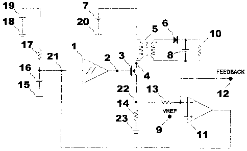
The present invention is a spike converter providing a special mode of
operation of a low power fly-back
converter in a very narrow duty cycle range in particular. This spike
operation minimizes the size of the
required reactive components such as that of the power transformer and output
capacitance. The present
invention automatically achieves low idle power consumption due to the nature
of the feedback under
fixed, narrow duty cycle or spike operation. The spike operation is defined by
the lower limit of the on time
of the switching element being generated by the sum of the propagation delays
of a current sense
comparator and an off time pulse generating comparator.

Revendications

Note : Les revendications sont présentées dans la langue officielle dans laquelle elles ont été soumises.


I claim as my invention:
1. A spike converter comprising:
(a) a DC bias supply having a positive and negative electrode where the
negative terminal is
connected to the common ground of the circuit;
(b) the positive terminal of said DC bias supply connected to one terminal of
a timing resistor;
(c) the other terminal of said timing resistor connected to one terminal of a
timing capacitor and
the input of a comparator with hysteresis and the output of a current sense
comparator;
(d) the other terminal of said timing capacitor connected to said common
ground;
(e) the output of said comparator with hysteresis connected to the gate
terminal of a switching
element, such as a MOSFET;
(f) the source terminal of said switching element connected to one terminal of
a sensing resistor
and one terminal of a current sample feed resistor;
(f) the other terminal of said sensing resistor connected to said common
ground;
(g) the other terminal of said current sample feed resistor connected to the
negative input of the
current sense comparator forming the feedback point of the converter;
(h) the positive terminal of said current sense comparator forming the voltage
reference point of
the converter;
(i) the drain terminal of said switching element connected to one terminal of
the primary
winding of a transformer;
(j) said transformer having a primary and secondary winding;
(k) the other terminal of said primary winding of said transformer connected
to the positive
terminal of the converter's DC power source;
(l) the negative terminal of the converter's DC power source connected to said
common ground;
(m) one terminal of the secondary winding of said transformer connected to the
anode of an
output rectifier;
(n) the cathode of said output rectifier forming the positive output of the
converter;
(o) the other terminal of said secondary winding of said transformer forming
the negative output
of the converter;
6

(p) an output capacitor connected between said positive and negative output
terminals;
(q) an output load in parallel with said output capacitor;
2. A spike converter as in claim 1, wherein said current sense comparator has
an output
substantially opened when the positive input is higher than the negative
input.
3. A spike converter as in claim 1, wherein the off time of said switching
element is determined by
said timing resistor and said timing capacitor.
4. A spike converter as in claim 1, wherein the on time of said switching
element is determined by
the amount of time it takes the current slope in said current sense resistor
to reach the value
defined by said voltage reference and said feedback.
5. A spike converter as in claim 1, wherein the on time of said switching
element is substantially
smaller than the off time thereby reducing said transformer and output
capacitor rating
requirements and therefore size.
6. A spike converter as in claim 1, wherein the on time of said switching
element is substantially
smaller than the off time keeping the reflected voltage on the switching
element low and thereby
reducing the required voltage handling capacity of same.
7. A spike converter as in claim 1, wherein the lower limit of the on time of
said switching element
is defined by the sum of the propagation delays of said comparator with
hysteresis and said
current sense comparator whereby said feedback forces the converter to enter
into pulse
skipping mode under light conditions.
8. A spike converter as in claim 7, wherein said pulse skipping mode causes
the converter to
consume very little power under said light load conditions.
7

Description

Note : Les descriptions sont présentées dans la langue officielle dans laquelle elles ont été soumises.


CA 02567462 2006-11-08
SPIKE CONVERTER
BACKGROUND OF THE INVENTION
1. Field of the Invention
The present invention generally relates to power converters. Specifically, the
present invention relates to
power converters for applications where power requirements are on the order of
a few watts. More
specifically, the present invention relates to those power converters having a
universal input voltage range
and needing to meet the requirements of "green" power, very low power
consumption, under light load
conditions.
2. Description of the Prior Art
Prior art embodiments customarily use a light or no load detection system by
sensing one of the parameters
related to loading and then initiating burst mode operation to reduce standby
power and to increase light
load efficiency. One such embodiment is a method whereby a comparator is used
to monitor a feedback
voltage relative to a reference level which, if exceeded, causes a burst mode
block to be activated in order
to keep idle power consumption low. Customarily, the starting point of a prior
art converter design is to set
the duty cycle around 50% for low line full load conditions which
unnecessarily increases the size and cost
of the components and thus the converter for low power applications.

CA 02567462 2006-11-08
SUMMARY OF THE INVENTION
The present invention exploits the advantages of spike mode operation which is
essentially a very low duty
cycle mode of operation of a fl,v-back converter with automatic pulse skipping
mode resulting in significant
size and cost reduction of the reactive con7ponents such as the power
transformer the output capacitance as
well as the de-rating of the switching eleinent. The present invention
provides a highly efficient power
converter for low power applications. Its low duty cycle allows the converter
to function at a lower
frequency while retaining the benefit of high frequency operation in the
selection of transformer where the
transfoimer size can be reduced to those used at frequencies several titnes
greater than here employed.
Additionally, the low duty cycle permits the reduction of the voltage rating
of the switching element,
typically a MOSFET, by approximately 20% and the current rating of the output
rectifier reducing size and
cost over prior art embodiments. Further, the present invention is practical
for low power applications such
as mobile phone chargers wherein reduced size, cost, and idle power
consumption are desirable thus
providing a superior alternative to the prior art.
2

CA 02567462 2006-11-08
BRIEF DESCRIPTION OF DRAWINGS
Figure 1 is a schematic diagram of the preferred embodiment of the present
invention.
Figure 2 is an illustration of a voltage waveform developed under operation at
one of the junction points
referenced in Figure 1 essential to the understanding of the present
invention.
Figure 3 is another illustration of a voltage wavefonn developed under
operation at one of the junction
points referenced in Figure 1 essential to the understanding of the present
invention.
Figure 4 is yet another illustration of a voltage waveform developed under
operation at one of the junction
points referenced in Figure 1 essential to the understanding of the present
invention.
Figure 5 is yet another illustration of a voltage waveform developed under
operation at one of the junction
points referenced in Figure 1 essential to the understanding of the present
invention.
Figure 6 is an illustration of a current waveform developed under operation at
one of the junction points
referenced in Figure 1 essential to the understanding of the present
invention.
DETAILED DESCRIPTION OF THE PREFERRED EMBODIMENT
In order to better understand the embodiment of the present invention, a spike
converter will be
described with reference to FIGURE 1 and corresponding waveforms in FIGURES 2
through 6. One
ternninal of a timing capacitor 16 is connected to a tiuning resistor 17 as in
FIGURE 1. The junction of said
timing capacitor 16 and timing resistor 17 is further connected to the input
of a comparator with hysteresis
1 and the output of a current sense comparator 11. A waveform as in FIGURE 3
is developed at junction
point 21. The other terminal of said timing resistor 17 is connected to the
positive terminal of a bias supply
19 and the other terminal of said timing capacitor 16 is connected to the
common ground 15. Ground points
15, 18, 20 and 23 represent a common point and are only separated for the
purposes of this illustration. The
negative terminal of bias supply 19 is connected to common ground 18.
3

CA 02567462 2006-11-08
The output of the comparator with hysteresis 1 is connected to the input
terminal of a switching
element 3, such as a MOSFET, forming the junction point 2 where a waveform as
in FIGURE 4 is
developed. The drain terminal of switching element 3 is connected to a
tenninal of the primary winding of
transformer 5 forming junction point 4 where a waveform as in FIGURE 5 is
developed. The other
terminal of said primary winding of transformer 5 is connected to the positive
terminal of the converter's
DC power source 7, a power source typically derived from rectified and
tiltered AC mains. The negative
tenninal of said DC power source 7 is connected to common ground 20.
The source terminal of switching element 3 is connected to a terminal of
sensing resistor 14 and
the a terminal of a current sample feed resistor 13 forming junction point 22.
A waveform as in FIGURE 2
is developed at junction point 22. The remaining terminal of said current
sample feed resistor 13 is
connected to the negative input of current sense comparator I1 fonning
feedback point 12. The remaining
terminal of sensing resistor 14 is connected to common ground 23. The positive
input of said current sense
comparator 11 forms voltage reference point 9.
A terminal of the secondary -Mnding of transformer 5 is connected to a
terminal of output
capacitor 8 and a terminal of load 10 forming the negative output of the
converter. The remaining terminal
of the secondary winding of transfontter 5 is connected the anode of rectifier
6. The cathode of said
rectifier 6 is connected to the remaining terminals of output capacitor 8 and
load 10 forming the positive
output of the converter. A current waveform as in FIGURE 6 is developed across
rectifier 6.
The operation of the spike converter will be described with reference to
FIGURE 1 and
corresponding wavefonns in FIGURES 2 and 3. iJnder full load and low line
condition, the voltage at the
gate terminal of switching element 3 remains zero until the voltage across
timing capacitor 16 reaches the
high threshold of comparator with hysteresis 1. Once the high threshold of
comparator with hysteresis I is
attained, the switching element 3 is turned on and cuirent ramps up with slope
VL where V is the supply
voltage and L is the inductance of the primary winding of transformer 5. Once
the ramp across the sensing
resistor 14 reaches the reference voltage as depicted by the VREF line in
FIGURE 2, current sense
comparator 11 will discharge timing capacitor 16 to the low threshold of
comparator with hysteresis 1
causing this cycle to begin again. The off time of the converter, as depicted
by the duration of tOFF in
FIGURE 2, is defined by the charge time of timing capacitor 16 via timing
resistor 17 from VLow to
4

CA 02567462 2006-11-08
VgicH> as depicted by FIGURE 3.
Since the on time of the converter, as depicted by the duration of tON in
FIGURE 2, is very brief
relative to the off time of the converter, the current feedback provides
excellent line regulation at full load.
At light load, the feedback is used to lower the current ramp threshold to
reduce the average
power. At some point under light load condition, the converter will enter into
small duty cycle mode where
the lower limit of the on time is defined by the sum of the propagation delays
of the comparators I and 11.
At this point, the current will only ramp up to the value it reaches within
the aforesaid time delay and the
feedback voltage on the negative input of current sense comparator 11 will
exceed the reference voltage for
much of the off time resulting in an extremely low duty cycle that allows the
converter to meet "green"
power specifications.
5

Dessin représentatif
Une figure unique qui représente un dessin illustrant l'invention.
États administratifs

2024-08-01 : Dans le cadre de la transition vers les Brevets de nouvelle génération (BNG), la base de données sur les brevets canadiens (BDBC) contient désormais un Historique d'événement plus détaillé, qui reproduit le Journal des événements de notre nouvelle solution interne.

Veuillez noter que les événements débutant par « Inactive : » se réfèrent à des événements qui ne sont plus utilisés dans notre nouvelle solution interne.

Pour une meilleure compréhension de l'état de la demande ou brevet qui figure sur cette page, la rubrique Mise en garde , et les descriptions de Brevet , Historique d'événement , Taxes périodiques et Historique des paiements devraient être consultées.

Historique d'événement

Description Date
Le délai pour l'annulation est expiré 2012-11-08
Demande non rétablie avant l'échéance 2012-11-08
Inactive : Demande ad hoc documentée 2012-08-10
Inactive : Abandon.-RE+surtaxe impayées-Corr envoyée 2011-11-08
Réputée abandonnée - omission de répondre à un avis sur les taxes pour le maintien en état 2011-11-08
Requête pour le changement d'adresse ou de mode de correspondance reçue 2009-02-06
Demande publiée (accessible au public) 2008-05-08
Inactive : Page couverture publiée 2008-05-07
Inactive : CIB attribuée 2007-02-14
Inactive : CIB en 1re position 2007-02-14
Inactive : CIB attribuée 2007-02-14
Exigences de dépôt - jugé conforme 2006-12-19
Inactive : Certificat de dépôt - Sans RE (Anglais) 2006-12-19
Demande reçue - nationale ordinaire 2006-12-12
Déclaration du statut de petite entité jugée conforme 2006-11-08

Historique d'abandonnement

Date d'abandonnement Raison Date de rétablissement
2011-11-08

Taxes périodiques

Le dernier paiement a été reçu le 2010-11-08

Avis : Si le paiement en totalité n'a pas été reçu au plus tard à la date indiquée, une taxe supplémentaire peut être imposée, soit une des taxes suivantes :

  • taxe de rétablissement ;
  • taxe pour paiement en souffrance ; ou
  • taxe additionnelle pour le renversement d'une péremption réputée.

Veuillez vous référer à la page web des taxes sur les brevets de l'OPIC pour voir tous les montants actuels des taxes.

Historique des taxes

Type de taxes Anniversaire Échéance Date payée
Taxe pour le dépôt - petite 2006-11-08
TM (demande, 2e anniv.) - petite 02 2008-11-10 2008-09-29
TM (demande, 3e anniv.) - petite 03 2009-11-09 2009-10-07
TM (demande, 4e anniv.) - petite 04 2010-11-08 2010-11-08
Titulaires au dossier

Les titulaires actuels et antérieures au dossier sont affichés en ordre alphabétique.

Titulaires actuels au dossier
IVAN MESZLENYI
Titulaires antérieures au dossier
S.O.
Les propriétaires antérieurs qui ne figurent pas dans la liste des « Propriétaires au dossier » apparaîtront dans d'autres documents au dossier.
Documents

Pour visionner les fichiers sélectionnés, entrer le code reCAPTCHA :


Pour visualiser une image, cliquer sur un lien dans la colonne description du document. Pour télécharger l'image (les images), cliquer l'une ou plusieurs cases à cocher dans la première colonne et ensuite cliquer sur le bouton "Télécharger sélection en format PDF (archive Zip)" ou le bouton "Télécharger sélection (en un fichier PDF fusionné)".

Liste des documents de brevet publiés et non publiés sur la BDBC .

Si vous avez des difficultés à accéder au contenu, veuillez communiquer avec le Centre de services à la clientèle au 1-866-997-1936, ou envoyer un courriel au Centre de service à la clientèle de l'OPIC.


Description du
Document 
Date
(aaaa-mm-jj) 
Nombre de pages   Taille de l'image (Ko) 
Abrégé 2006-11-08 1 14
Description 2006-11-08 5 154
Dessins 2006-11-08 2 26
Revendications 2006-11-08 2 68
Dessin représentatif 2008-04-21 1 9
Page couverture 2008-04-28 1 36
Certificat de dépôt (anglais) 2006-12-19 1 158
Avis de rappel: Taxes de maintien 2008-08-11 1 122
Avis de rappel: Taxes de maintien 2009-08-11 1 128
Avis de rappel: Taxes de maintien 2010-08-10 1 123
Rappel - requête d'examen 2011-07-11 1 119
Avis de rappel: Taxes de maintien 2011-08-09 1 121
Courtoisie - Lettre d'abandon (taxe de maintien en état) 2012-01-03 1 172
Courtoisie - Lettre d'abandon (requête d'examen) 2012-02-14 1 165
Deuxième avis de rappel: taxes de maintien 2012-05-09 1 119
Avis de rappel: Taxes de maintien 2012-08-09 1 120
Correspondance 2006-12-19 1 11
Taxes 2008-09-29 1 26
Correspondance 2009-02-06 1 28
Taxes 2009-10-07 1 33
Taxes 2010-11-08 1 26