Note : Les descriptions sont présentées dans la langue officielle dans laquelle elles ont été soumises.
CA 02568123 2006-11-10
E-CC-00218 CA
Smart Card Body, Smart Card and Manufacturing Process for Same
The present invention relates to a smart card body, a smart card and a
manufacturing process for same, and in particular to smart cards used for
subscriber
identity modules (SIM) cards.
According to a conventional manufacturing process for a smart card, a smart
card
body and a chip card module are manufactured separately. The chip card module
is
normally embedded in the smart card body before the smart card body provided
with the
chip card module is cut out.
US 6,288,904 shows a chip card module that is incorporated in a smart card
body.
A chip is positioned on a circuit carrier and connected to contacts on the
opposite site of
the circuit carrier by means of wire bonds. The chip is enclosed in a frame
which is
surrounded with a filling to protect the chip and the wire bonds from
mechanical stress.
From US 5,147,982 an encapsulation process for a semiconductor chip in a
micromodule is known, wherein the micromodule can then be incorporated in a
card. A
pre-punched metallic layer is formed, a pre-perforated plastic layer is
applied to the
metallic layer and a semiconductor chip is positioned on the surface of the
metallic layer
in a perforation of the plastic layer. A protective ring, which surrounds the
chip, is filled
with protective material, for example a silicone resin.
In the case of the known manufacturing processes, the chip card modules and
smart card bodies are manufactured separately and the chip card module
manufactured
separately has to be incorporated in a smart card body to produce a smart
card, something
that results in a complicated manufacturing process.
The European patent application EP 1 554 754 describes a manufacturing process
for a data carrier, in particular for a GSM plug body, wherein a data carrier
is
manufactured on a carrier strip. The data carrier has a data carrier body,
which is
1734593_1 - 1 -
CA 02568123 2013-04-16
31255-1
provided with an electronic component, and the carrier strip has a large
number of carrier
elements. The manufacturing process comprises injection moulding around the
carrier
elements of the carrier strip to produce a large number of data carrier
bodies, and connection
of the electronic components to the data carrier bodies to produce a large
number of data
carriers.
In this manufacturing process for data carriers, the large number of data
carriers are manufactured with the electronic component incorporated in the
data carrier body
and the data carriers are manufactured on a single carrier strip so that it is
possible to reduce
the manufacturing costs. This manufacturing process for a data carrier is
however not flexible
enough as the data carrier is manufactured with the electronic component.
There is therefore a need for a flexible and simple manufacturing process for
a
smart card body and an assembly process for a smart card which are compatible
with a roll-to-
roll process.
Some aspects of the present disclosure seek to improve a process for the
manufacture of a smart card body and a process for the assembly of a smart
card in such a
manner that a simple and adaptable process can be achieved for the manufacture
of a smart
card.
According to an aspect of the present invention, there is provided a process
for
the manufacture of a smart card body for incorporating a semiconductor chip,
the process
comprising the steps of: forming a lead frame in a conductive layer, wherein
the lead frame
has a first contact on a first surface and can be connected to the
semiconductor chip on a
second surface opposite the first surface, and forming an electrically
insulating casing layer on
the second surface of the smart card body, wherein the casing layer has a
recess for
incorporating the semiconductor chip, wherein at least a portion of the casing
layer extends in
a direction toward the second surface from a position substantially coplanar
with the first
surface.
- 2 -
CA 02568123 2013-04-16
31255-1
According to another aspect of the present invention, there is provided a
process for the assembly of a smart card, the process comprising the steps of:
fitting a
semiconductor chip in a recess in a casing layer of a smart card body
manufactured according
to the process described above, and closing the recess in the casing layer of
the smart card
body.
According to another aspect of the present invention, there is provided a
smart
card body for incorporating a semiconductor chip, the smart card body
comprising: a
conductive layer, which is structured in such a manner that it forms a lead
frame that has first
contacts on a first surface and can be connected to the semiconductor chip on
a second surface
opposite the first surface, wherein the smart card body has on its second
surface an electrically
insulating casing layer with a recess for incorporating a semiconductor chip,
wherein at least a
portion of the casing layer extends in a direction toward the second surface
from a position
substantially coplanar with the first surface.
According to another aspect of the present invention, there is provided a
carrier
strip comprising a plurality of smart card bodies described above, wherein the
plurality of
smart card bodies are detachable from the carrier strip.
According to another aspect of the present invention, there is provided a
smart
card comprising a semiconductor chip, which is affixed in the recess in the
casing layer of the
smart card body described above, and a surface layer to close the recess in
the casing layer of
the smart card body.
According to some embodiments, a process for the manufacture of a smart card
body for incorporating a semiconductor chip is described, wherein the process
comprises the
formation of a lead frame in a conductive layer, wherein the lead frame has on
a first surface
first contacts for connection to an external component, such as a mobile
telephone or similar
item, and can be connected to the semiconductor chip on a second surface
opposite the first
surface. According to some embodiments, the process comprises the formation of
a casing
layer made of insulating material, for example injection-moulded material, on
the second
- 3 -
CA 02568123 2013-04-16
. 31255-1
surface of the smart card body, wherein the casing layer has a recess for
incorporating the
semiconductor chip.
The process thus manufactures a smart card body which is adapted to
incorporate a semiconductor chip. Incorporation of the semiconductor chip does
not take
place until the assembly of a smart card, which comprises a smart card body
and a
semiconductor chip incorporated therein. According to some embodiments, a
process is thus
described wherein a smart card body, which does not yet contain a
semiconductor chip, is
manufactured. This has the advantage that the manufacture of a smart card can
take place in a
particularly flexible manner.
The possibility of not only manufacturing a smart card body but also
performing the assembly of a smart card by means of a roll-to-roll process
also makes the
manufacture of a smart card particularly simple. A roll of smart card bodies
can be simply
supplied to a smart card manufacturer, who then only needs to install the
semiconductor chips
and close the smart card bodies provided with the semiconductor chips as the
final process
steps. In addition, the personalization of a smart card can be carried out by
the smart card
manufacturer using a roll-to-roll-process by laminating a personalized strip
onto the smart
card bodies provided with the semiconductor chips.
The manufacture of a smart card is also particularly simplified because the
smart card manufacturer no longer has to carry out the steps involving
detachment of the
smart card module and embedding of the smart card module in the smart card
body as
necessary in the conventional manufacturing processes. According to some
embodiments, the
smart card body is manufactured by means of a roll-to-roll-process so that
only the
semiconductor chip needs to be installed and the smart card body closed to
produce a smart
card. The smart card manufacturer can also make use of his existing roll-to-
roll processes.
In addition, the smart card body according to some embodiments can also be
incorporated in another larger smart card body. This is particularly
advantageous when the
smart card body is manufactured according to the 3FF smart card format, which
represents a
smart card format with reduced dimensions in comparison with the 1FF and 2FF
smart card
- 4 -
CA 02568123 2013-04-16
. 31255-1
formats. A 3FF smart card body can thus be incorporated in another 1FF or 2FF
smart card
body, something that offers a smart card manufacturer even greater flexibility
in smart card
manufacturing.
It is particularly advantageous when the step involving the formation of a
lead
frame comprises the punching-out of the conductive layer, preferably
consisting of copper,
and the metallization, preferably by electroplating, of the punched-out
conductive layer. A
roll of copper can thus be punched out and metallized using a roll-to-roll
process to produce a
lead frame in a simple and low-cost manner.
When the second surface of the conductive layer is provided with second
contacts, preferably made of gold, wherein the second contacts are used for
contacting of the
semiconductor chip to be incorporated, the semiconductor chip to be
incorporated can easily
be electrically connected to the lead frame.
When the casing layer is formed from an insulating injection-moulded
material, wherein a pre-punched dielectric layer is laminated onto the second
surface of the
conductive layer, and plastics material is injection-moulded around the
laminated conductive
layer, it is possible to manufacture the casing layer in a simple and low-cost
manner. In
addition, this has the advantage that only one surface layer needs to be
arranged on the casing
layer in a subsequent process step once a semiconductor chip has been
incorporated in the
recess of the casing layer to produce a smart card. The process for the
assembly of a smart
card is thus simplified.
It is particularly advantageous to manufacture a large number of smart card
bodies on a carrier strip, wherein the large number of smart card bodies can
be detached from
the carrier strip. The process for the manufacture of a smart card body is
thus compatible with
a roll-to-roll process, something that provides for a simple and low-cost
manufacturing
process. The large number of smart card bodies is manufactured on a roll and
can be supplied
to a smart card manufacturer, who then only has to fit a semiconductor chip in
the smart card
body and close the smart card body to produce a smart card.
- 5 -
CA 02568123 2013-04-16
. 31255-1
According one aspect, a process for the assembly of a smart card is described,
wherein the process comprises the fitting of a semiconductor chip in the
recess of the casing
layer of the manufactured smart card body and closing of the recess in the
casing layer of the
smart card body.
A smart card is thus manufactured in a simple and low-cost manner. In
addition, the process for the assembly of a smart card offers a smart-card
manufacturer the
advantage that the manufacture of a smart card can be carried out more
quickly, above all
when the smart cards are manufactured by means of a roll-to-roll process. As
the smart card
bodies are supplied on a roll ready for use, it is only necessary to fit the
semiconductor chip in
the smart card body and to close the smart card body in order to manufacture
the smart card.
The surface layer of the smart card body can also be personalized, for example
provided with
labeling.
It is particularly advantageous when closing of the recess in the casing layer
of
the smart card body comprises the lamination of a strip over the recess. It is
thus possible to
close the smart card bodies in a simple, fast and low-cost manner.
Examples of embodiments of the invention are explained in greater detail
below by means of the designs shown in the attached drawings. Similar or
corresponding
details of the smart card body according to the various embodiments are
provided with the
same reference signs in the figures. The following are shown:
Fig. 1 a top view of a first side of a carrier strip, which is at a first step
of the
manufacturing process for a smart card body according to an embodiment of the
present
invention;
Fig. 2 a top view of a first side of a carrier strip, which is at a second
step of
the manufacturing process for a smart card body according to an embodiment of
the present
invention;
- 6 -
CA 02568123 2013-04-16
. 31255-1
Fig. 3 a top view of a first side of a carrier strip, which is at a third step
of the
manufacturing process for a smart card body according to an embodiment of the
present
invention;
Fig. 4 a top view of a second side of the carrier strip shown in Fig. 3;
Fig. 5 a sectional view through the carrier strip shown in Fig. 4 along the
section line A-A;
Fig. 6 an enlarged view of the section shown in Fig. 5.
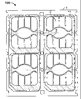
Figs. 1, 2 and 3 show a top view of a first surface of a carrier strip. Fig. 4
shows a top view of a second surface opposite the first surface. Figs. 1, 2
and 3 and Fig. 4
thus show top views of the two sides of the smart card body according to an
embodiment of
the invention.
As can be seen from Fig. 1, a large number of smart card bodies 10 are
manufactured on a carrier strip 100. The carrier strip 100 is formed by a
conductive layer 1,
which preferably consists of copper sheeting. Other conductive materials are
however also
possible, for example aluminum. The carrier strip 100 preferably consists of a
roll of
- 6a -
CA 02568123 2006-11-10
E-CC-00218 CA
the conductive layer 1 so that the large number of smart card bodies 10 can be
manufactured by means of a roll-to-roll process.
The process for the manufacture of a smart card body 10 for incorporating a
semiconductor chip is explained with the help of Figs. 1, 2 and 3.
First of all the conductive layer 1 is punched out, and a lead frame formed in
the
conductive layer 1. On a first surface of the conductive layer 1, which is
shown in Fig. 1,
the lead frame has first contacts 2, and the conductive layer 1 is punched out
along the
roll by a punching tool (shown in Fig. 1 by the black punch-outs). As can be
seen from
Figs. 1, 2 and 3, two smart card bodies 10 are manufactured within a single
width of the
conductive roll. It is of course also possible to select a different number of
smart card
bodies within the width of the roll.
Once the conductive layer 1 has been punched out and the lead frame formed,
the
contacts 2 arranged on the first surface are metallized. The first contacts 2
are preferably
coated with nickel and nickel-phosphorus using an electroplating process.
Other
metallization processes for the punched-out conductive layer 1 are however
also possible,
for example sputtering, vapor-deposit or such methods. The second surface of
the
conductive layer 1 (not shown in Figs. 1, 2 and 3) is provided with second
contacts 13,
which are preferably made of gold. These second contacts 13 are used to
connect the
semiconductor chip to be incorporated with the first contacts 2 of the lead
frame. The
semiconductor chip is preferably connected to the second contacts 13 via wire
bonds.
A pre-punched dielectric layer (not shown in Figs. 1, 2 and 3) is then
laminated
onto the second surface of the conductive layer 1. The dielectric layer is pre-
punched in
such a manner that the second contacts 13 correspond to the punch-outs of the
dielectric
layer.
The dielectric layer is then activated by means of a laser treatment, wherein
said
laser treatment increases the roughness of the surface of the dielectric
layer. This process
1734593_1 - 7 -
CA 02568123 2006-11-10
E-CC-00218 CA
step is necessary to ensure that the injection-moulded plastics material
applied in a
subsequent process step adheres to the surface of the dielectric layer.
As can be seen from Fig. 2, punching dies punch out the carrier strip 100
(shown
by the black punch-outs), thus creating the form of the smart card body 10.
According to an advantageous embodiment of the present invention two smart
card bodies 10 are manufactured within a single width of the roll and a
punching tool
punches out the first half of each of two first smart card bodies while a
second punching
tool punches out the second half of each of two second smart card bodies, as
can be seen
from Fig. 2. Movement along the roll thus allows the two halves of two smart
card bodies
to be punched out within one width of the roll and the form of the smart card
body to be
created.
As can be seen from Fig. 3, a casing layer 11 is then formed from insulating
injection-moulded material on the second surface of the smart card body. Here
plastic
material is injection-moulded around the laminated conductive layer 1. The
injection-
moulded casing layer 11 thus forms an edge on all sides of the smart card body
10 both
around the first and the second contacts 2, 13, and the smart card body 10 so
formed
preferably corresponds to the format of a 3FF smart card.
Fig. 4 shows a top view of the second surface of the smart card body 10 and
Fig. 5
shows a section through the carrier strip 100 along the section line A-A shown
in Fig. 4.
Fig. 6 shows an enlarged view of detail VI of the section shown in Fig. 5.
As can be seen from Fig. 4, the casing layer 11 has a recess 12 for
incorporating a
semiconductor chip. The second contacts 13 are arranged on the conductive
layer 1 and
the dielectric layer 14 laminated to the conductive layer 1 is pre-punched in
such a
manner that the second contacts 13 are accessible for contacting to a
semiconductor chip
to be incorporated.
1734593_1 - 8 -
CA 02568123 2006-11-10
E-CC-00218 CA
As can be seen from Figs. 5 and 6, the combined height of the casing layer 11
and
the surface layer (not shown in the figures), which is laminated onto the
casing layer 11 in
a subsequent process step for the assembly of a smart card, corresponds to the
thickness
of a smart card according to the 3FF format. The height of the casing layer 11
preferably
has a value H of 0.7 millimeters, while the thickness of the laminated surface
layer has a
value of 0.1 millimeters. As can be seen from Fig. 6, the height H of the
casing layer 11
encompasses the distance between the first surface of the injection-moulded
material
arranged level with the first surface of the conductive layer 1 and the second
surface of
the injection-moulded material, to which the surface layer is laminated.
The assembly of a smart card is explained in greater detail below.
A semiconductor chip is fitted in the recess 12 of the casing layer 11 of the
smart
card body 10. The semiconductor chip is preferably glued to the dielectric
layer 14.
Alternatively, the semiconductor chip can also be directly affixed to the
conductive layer
1. The recess 12 provided with the semiconductor chip in the casing layer 11
of the smart
card body 10 is then closed. A strip is preferably laminated onto the recess
12 in the
casing layer 11.
According to an advantageous embodiment of the present invention a large
number of smart card bodies 10 are manufactured on a carrier strip 100 by
means of a
roll-to-roll process. This simplifies the manufacturing process of a smart
card as a carrier
strip can be supplied to a smart card manufacturer, who then only needs to
carry out the
process steps involving installation of a semiconductor chip and closing of
the casing
layer 11. As the large number of smart card bodies 10 can be detached from the
carrier
strip 100, the smart cards only need to be separated after assembly.
The process for the manufacture of a smart card body according to the present
invention allows the manufacture of Subscriber Identity Module (SIM) cards to
be made
more flexible and simple. Smart card bodies 10 can be manufactured on a
carrier strip 100
1734593_1 - 9 -
CA 02568123 2006-11-10
E-CC-00218 CA
by means of a roll-to-roll process and such a carrier strip 100 can be
subsequently
supplied to a smart card manufacturer, who then only needs to install a
semiconductor
chip and close the smart card body to produce a smart card.
1734593j - 10 -