Sélection de la langue

Search

Sommaire du brevet 2571473 

Énoncé de désistement de responsabilité concernant l'information provenant de tiers

Une partie des informations de ce site Web a été fournie par des sources externes. Le gouvernement du Canada n'assume aucune responsabilité concernant la précision, l'actualité ou la fiabilité des informations fournies par les sources externes. Les utilisateurs qui désirent employer cette information devraient consulter directement la source des informations. Le contenu fourni par les sources externes n'est pas assujetti aux exigences sur les langues officielles, la protection des renseignements personnels et l'accessibilité.

Disponibilité de l'Abrégé et des Revendications

L'apparition de différences dans le texte et l'image des Revendications et de l'Abrégé dépend du moment auquel le document est publié. Les textes des Revendications et de l'Abrégé sont affichés :

  • lorsque la demande peut être examinée par le public;
  • lorsque le brevet est émis (délivrance).
(12) Demande de brevet: (11) CA 2571473
(54) Titre français: PROCEDE ET APPAREIL D'IMAGERIE CHIMIQUE SUR FOND SOMBRE
(54) Titre anglais: METHOD AND APPARATUS FOR DARK FIELD CHEMICAL IMAGING
Statut: Réputée abandonnée et au-delà du délai pour le rétablissement - en attente de la réponse à l’avis de communication rejetée
Données bibliographiques
(51) Classification internationale des brevets (CIB):
  • G01J 03/44 (2006.01)
  • G01N 21/65 (2006.01)
(72) Inventeurs :
  • TUSCHEL, DAVID (Etats-Unis d'Amérique)
  • HUTCHISON, WESLEY H. (Etats-Unis d'Amérique)
  • BERKMAN, MYLES P. (Etats-Unis d'Amérique)
(73) Titulaires :
  • CHEMIMAGE CORPORATION
(71) Demandeurs :
  • CHEMIMAGE CORPORATION (Etats-Unis d'Amérique)
(74) Agent: DIMOCK STRATTON LLP
(74) Co-agent:
(45) Délivré:
(86) Date de dépôt PCT: 2005-05-06
(87) Mise à la disponibilité du public: 2006-01-19
Requête d'examen: 2007-03-14
Licence disponible: S.O.
Cédé au domaine public: S.O.
(25) Langue des documents déposés: Anglais

Traité de coopération en matière de brevets (PCT): Oui
(86) Numéro de la demande PCT: PCT/US2005/016142
(87) Numéro de publication internationale PCT: US2005016142
(85) Entrée nationale: 2006-12-21

(30) Données de priorité de la demande:
Numéro de la demande Pays / territoire Date
10/879,636 (Etats-Unis d'Amérique) 2004-06-30

Abrégés

Abrégé français

L'invention porte d'une manière générale sur un procédé et un appareil fournissant l'image d'un échantillon. L'appareil comporte une source d'éclairage permettant de transférer des photons sur un échantillon. Les photons transférés éclairent l'échantillon ou sont diffusés lorsqu'ils frappent l'échantillon. Une lentille recueille les photons diffusés et les transfert sur un filtre accordable pour former une image. Les photons éclairants allant de la source lumineuse à l'échantillon ne passent pas par la lentille.


Abrégé anglais


The disclosure is generally directed to a method and apparatus for providing
an image of a sample. The apparatus includes an illuminating source for
transmitting photons to a sample. The transmitted photons illuminate the
sample or are scattered upon reaching the sample. A lens collects the
scattered photons and transmits the scattered photons to a tunable filter for
forming an image. The illuminating photons traveling from the illuminating
source to the sample do not pass through the lens.

Revendications

Note : Les revendications sont présentées dans la langue officielle dans laquelle elles ont été soumises.


What is claimed is:
1. A method for obtaining a spatially accurate wavelength-resolved image of a
sample, the method comprising the steps of:
providing a sample;
illuminating the sample with a plurality of photons to thereby produce photons
scattered by the sample; and
collecting the scattered photons through an optical device to thereby obtain a
spatially accurate wavelength-resolved image of the sample,
wherein the illuminating photons do not pass through the optical device.
2. The method of Claim 1 wherein the scattered photons include photons
emitted by the sample.
3. The method of Claim 1 wherein the wavelength-resolved image includes a
Raman image.
4. The method of Claim 1 wherein the wavelength-resolved image includes a
luminescence emission image.
5. The method of Claim 1 wherein the step of collecting the scattered photons
includes collecting scattered photons having a wavelength in a predetermined
wavelength
band.

6. The method of Claim 5 wherein the step of collecting the scattered photons
includes obtaining plural sets of scattered photons,
wherein each set of scattered photons contains photons in a predetermined
wavelength band different from the predetermined wavelength band of the other
sets of
scattered photons, and
wherein a spatially accurate wavelength-resolved image of the sample is
obtained
from each set of scattered photons.
7. The method of Claim 1 wherein the step of collecting the scattered photons
occurs during a predetermined time interval.
8. The method of Claim 6 wherein during said time interval the sample
undergoes a change selected from the group of changes consisting of: spatial
displacement, chemical interaction, chemical state, phase, growth, shrinkage,
chemical
decomposition, chemical metabolization, and physical strain.
9. The method of Claim 1 wherein the step of illuminating the sample
includes illuminating the sample with photons that travel at an angle that is
oblique to a
plane along which the sample is substantially oriented.
10. The method of Claim 1 wherein the wavelength of the scattered photons is
different than the wavelength of the illuminating photons.
11. The method of Claim 1 wherein the step of illuminating the sample
includes illuminating a side of the sample opposite the optical device.
12. The method of Claim 1 wherein the step of illuminating the sample
includes photons from an evanescence light source.
11

13. The method of Claim 1 wherein the step of collecting scattered photons
includes collecting scattered polarized photons.
14. The method of Claim 1 wherein the step of collecting scattered photons
includes collecting scattered un-polarized photons.
15. The method of Claim 1 further comprising the step of filtering the
collected
photons though an optical filter.
16. The method of Claim 1 further comprising the step of spectrally separating
the collected photons.
17. A system for obtaining a spatially accurate wavelength-resolved image of a
sample, comprising:
a sample;
a photon emission source for illuminating the sample with a plurality of
photons to
thereby produce photons scattered by the sample;
an optical lens for collecting the scattered photons;
a filter for receiving the collected scattered photons and providing therefrom
filtered photons; and
a charged couple device for receiving the filtered photons and obtaining
therefrom
a spatially accurate wavelength-resolved image of the sample,
wherein the illuminating photons do not pass through the optical lens.
18. The method of Claim 17 wherein the scattered photons include photons
emitted by the sample.
12

19. The method of Claim 17 wherein the wavelength-resolved image includes a
Raman image.
20. The method of Claim 17 wherein the wavelength-resolved image includes a
luminescence emission image.
21. The method of Claim 17 wherein the step of collecting the scattered
photons includes collecting scattered photons having a wavelength in a
predetermined
wavelength band.
22. The method of Claim 21 wherein the step of collecting the scattered
photons includes obtaining plural sets of scattered photons,
wherein each set of scattered photons contains photons in a predetermined
wavelength band different from the predetermined wavelength band of the other
sets of
scattered photons, and
wherein a spatially accurate wavelength-resolved image of the sample is
obtained
from each set of scattered photons.
23. The method of Claim 17 wherein the step of collecting the scattered
photons occurs during a predetermined time interval.
24. The method of Claim 22 wherein during said time interval the sample
undergoes a change selected from the group of changes consisting of spatial
displacement, chemical interaction, chemical state, phase, growth, shrinkage,
chemical
decomposition, chemical metabolization, and physical strain.
25. The method of Claim 17 wherein the step of illuminating the sample
includes illuminating the sample with photons that travel at an angle that is
oblique to a
plane along which the sample is substantially oriented.
13

26. The method of Claim 17 wherein the wavelength of the scattered photons is
different than the wavelength of the illuminating photons.
27. The method of Claim 17 wherein the step of illuminating the sample
includes a side of the sample opposite the optical device.
28. The method of Claim 17 wherein the step of illuminating the sample
includes photons from an evanescence light source.
29. The method of Claim 17 wherein the step of collecting scattered photons
includes collecting scattered polarized photons.
30. The method of Claim 17 wherein the step of collecting scattered photons
includes collecting scattered un-polarized photons.
31. The method of Claim 17 further comprising the step of filtering the
collected photons though an optical filter.
32. The method of Claim 17 further comprising the step of spectrally
separating the collected photons.
33. The system of Claim 17 wherein the tunable filter includes one or more
photonic crystals, a mirror, a solid state optical device and a micromachined
tunable
filter.
34. The system of Claim 17 wherein the filter is a tunable filter.
35. The system of Claim 34 wherein the tunable filter is an optical filter.
36. The system of Claim 17 further comprising a notch filter interposed
between the optical lens and the filter.
14

37. The system of Claim 17 wherein the photon illumination source is
positioned at an angle with respect to an axis formed by the sample and the
filer.
38. The device of Claim 17 wherein the one or more wavelength-resolved
images of a sample defines a Raman image.
39. An apparatus for forming an image of a sample comprising:
a photon transmitter for transmitting a plurality of illuminating photons to a
sample;
said sample for producing scattered photons from said plurality of
illuminating
photons;
a lens for collecting the scattered photons and forming the image of the
sample;
and
a tunable filter for receiving the collected photons therefrom,
wherein the photon transmitter, the sample and the tunable filter are
positioned
relative to each other so that the angle between the illuminating photons and
the scattered
photons forms an oblique angle.
40. The apparatus of Claim 39 wherein the scattered photons include photons
emitted by the sample.
41. The apparatus of Claim 39 further comprising an optical filter interposed
between the tunable filter and the lens.
42. The apparatus of Claim 39 wherein the lens collects substantially none of
the illuminated photons.
43. The apparatus of Claim 39 wherein the formed image is a Raman image.

44. The apparatus of Claim 39 wherein the tunable filter is a liquid crystal
tunable filter.
45. The apparatus of Claim 39 further comprising a charged couple device.
46. The apparatus of Claim 39 wherein the formed image is a luminescence
emission image.
47. A method for obtaining a spatially accurate wavelength-resolved image of a
sample, the method comprising the steps of:
providing a sample;
illuminating the sample with a plurality of photons to thereby produce photons
emitted by the sample; and
collecting the emitted photons through an optical device to thereby obtain a
spatially accurate wavelength-resolved image of the sample,
wherein the illuminating photons do not pass through the optical device.
48. The method of Claim 47 wherein the wavelength-resolved image includes a
Raman image.
49. The method of Claim 47 wherein the wavelength-resolved image includes a
luminescence emission image.
50. The method of Claim 47 wherein the step of collecting the emitted photons
includes collecting emitted photons having a wavelength in a predetermined
wavelength
band.
16

51. The method of Claim 50 wherein the step of collecting the emitted photons
includes obtaining plural sets of emitted photons,
wherein each set of emitted photons contains photons in a predetermined
wavelength band different from the predetermined wavelength band of the other
sets of
emitted photons, and
wherein a spatially accurate wavelength-resolved image of the sample is
obtained
from each set of emitted photons.
52. The method of Claim 47 wherein the step of collecting the emitted photons
occurs during a predetermined time interval.
53. The method of Claim 51 wherein during said time interval the sample
undergoes a change selected from the group of changes consisting of: spatial
displacement, chemical interaction, chemical state, phase, growth, shrinkage,
chemical
decomposition, chemical metabolization, and physical strain.
54. The method of Claim 47 wherein the step of illuminating the sample
includes illuminating the sample with photons that travel at an angle that is
oblique to a
plane along which the sample is substantially oriented.
55. The method of Claim 47 wherein the wavelength of the emitted photons is
different than the wavelength of the illuminating photons.
56. The method of Claim 47 wherein the step of illuminating the sample
includes illuminating a side of the sample opposite the optical device.
57. The method of Claim 47 wherein the step of illuminating the sample
includes photons from an evanescence light source.
17

58. The method of Claim 47 wherein the step of collecting emitted photons
includes collecting emitted polarized photons.
59. The method of Claim 47 wherein the step of collecting emitted photons
includes collecting emitted un-polarized photons.
60. The method of Claim 47 further comprising the step of filtering the
collected photons though an optical filter.
61. The method of Claim 47 further comprising the step of spectrally
separating the collected photons.
62. A system for obtaining a spatially accurate wavelength-resolved image of a
sample, comprising:
a sample;
a photon emission source for illuminating the sample with a plurality of
photons to
thereby produce photons emitted by the sample;
an optical lens for collecting the emitted photons;
a filter for receiving the collected emitted photons and providing therefrom
filtered
photons; and
a charged couple device for receiving the filtered photons and obtaining
therefrom
a spatially accurate wavelength-resolved image of the sample,
wherein the illuminating photons do not pass through the optical lens.
63. The method of Claim 62 wherein the wavelength-resolved image includes a
Raman image.
18

64. The method of Claim 62 wherein the wavelength-resolved image includes a
luminescence emission image.
65. The method of Claim 62 wherein the/step of collecting the emitted photons
includes collecting emitted photons having a wavelength in a predetermined
wavelength
band.
66. The method of Claim 65 wherein the step of collecting the emitted photons
includes obtaining plural sets of emitted photons,
wherein each set of emitted photons contains photons in a predetermined
wavelength band different from the predetermined wavelength band of the other
sets of
emitted photons, and
wherein a spatially accurate wavelength-resolved image of the sample is
obtained
from each set of emitted photons.
67. The method of Claim 62 wherein the step of collecting the emitted photons
occurs during a predetermined time interval.
68. The method of Claim 66 wherein during said time interval the sample
undergoes a change selected from the group of changes consisting of spatial
displacement, chemical interaction, chemical state, phase, growth, shrinkage,
chemical
decomposition, chemical metabolization, and physical strain.
69. The method of Claim 62 wherein the step of illuminating the sample
includes illuminating the sample with photons that travel at an angle that is
oblique to a
plane along which the sample is substantially oriented.
70. The method of Claim 62 wherein the wavelength of the emitted photons is
different than the wavelength of the illuminating photons.
19

71. The method of Claim 62 wherein the step of illuminating the sample
includes a side of the sample opposite the optical device.
72. The method of Claim 62 wherein the step of illuminating the sample
includes photons from an evanescence light source.
73. The method of Claim 62 wherein the step of collecting emitted photons
includes collecting emitted polarized photons.
74. The method of Claim 62 wherein the step of collecting emitted photons
includes collecting emitted un-polarized photons.
75. The method of Claim 62 further comprising the step of filtering the
collected photons though an optical filter.
76. The method of Claim 62 further comprising the step of spectrally
separating the collected photons.
77. The system of Claim 62 wherein the tunable filter includes one or more
photonic crystals, a mirror, a solid state optical device and a micromachined
tunable
filter.
78. The system of claim by. wherein the filter is a tunable filter.
79. The system of Claim 78 wherein the tunable filter is an optical filter.
80. The system of Claim 62 further comprising a notch filter interposed
between the optical lens and the filter.
81. The system of Claim 62 wherein the photon illumination source is
positioned at an angle with respect to an axis formed by the sample and the
filer.

82. The device of Claim 62 wherein the one or more wavelength-resolved
images of a sample defines a Raman image.
83. An apparatus for forming an image of a sample comprising:
a photon transmitter for transmitting a plurality of illuminating photons to a
sample;
said sample for producing emitted photons from said plurality of illuminating
photons;
a lens for collecting the emitted photons and forming the image of the sample;
and
a tunable filter for receiving the collected photons therefrom,
wherein the photon transmitter, the sample and the tunable filter are
positioned
relative to each other so that the angle between the illuminating photons and
the emitted
photons forms an oblique angle.
84. The apparatus of Claim 83 further comprising an optical filter interposed
between the tunable filter and the lens.
85. The apparatus of Claim 83 wherein the lens collects substantially none of
the illuminated photons.
86. The apparatus of Claim 83 wherein the formed image is a Raman image.
87. The apparatus of Claim 83 wherein the tunable filter is a liquid crystal
tunable filter.
88. The apparatus of Claim 83 further comprising a charged couple device.
21

89. The apparatus of Claim 83 wherein the formed image is a luminescence
emission image.
22

Description

Note : Les descriptions sont présentées dans la langue officielle dans laquelle elles ont été soumises.


CA 02571473 2006-12-21
WO 2006/007065 PCT/US2005/016142
Method and Apparatus for Dark Field Chemical Imaging
Related Applications
[0001] The instant disclosure claims the filing-date benefit of Application
Serial
Nos. 10/698,243 and 10/698,584 filed October 31, 200, as well as provisional
application
No. 60/422,604 filed October 31, 2002, each of which is incorporated herein by
reference
in its entirety. In addition cross-reference is made to U.S. Application
Serial No.
filed concurrently herewith and entitled Method and Apparatus for Dynamic
Chemical
Imaging which is also incorporated herein in its entirety for background
information.
Background
[0002] Conventional spectroscopic imaging systems are generally based on the
application of high resolution, low aberration, lenses and systems that
produce images
suitable for visual resolution by a human eye. These imaging systems include
both
microscopic spectral imaging systems as well as macroscopic imaging systems
and use
complex multi-element lenses designed for visual microscopy with high
resolution
aberrations optimized for each desired magnification. However, transmitting
illumination through such complex lenses attenuates the incident beam and
creates
spurious scattered light.
[0003] Further, each lens magnification results in a particular collection
angle for
the scattered light. Generally, at lower magnification the collection
efficiency is strongly
reduced as the focal distance increases. Consequently, the lens must be placed
further
away from the sample. For macro-systems (i.e., systems needing a broader view
of the
larger sample rather than a high magnification of a smaller portion of the
sample), the
reduced collection aperture severely limits the collected signal. The need for
high
collection efficiency may be critical for spectroscopic imaging at all
distances.
1

CA 02571473 2006-12-21
WO 2006/007065 PCT/US2005/016142
[0004] Much of the optical signal detected in the conventional systems is
dramatically reduced because of the system configuration and the need to
maintain high
resolution by removing optical aberrations. Conventional systems have been
largely
conceived based on the premises and the requirements of optical microscopy.
Namely,
the need to present a high resolution, zero-aberration, image to the operator
who uses
visual inspection to perceive the image. In addition, conventional micro-Raman
systems
achieve their high spatial resolution through the focus of the laser beam to a
diffraction-
limited spot by the microscope's objective lens. These design premises and
system
configurations limit the light -delivery in conjunction with the collection
efficiency of the
spectroscopic imaging system.
[0005] . Finally, design premises based on resolution and throughput
requirements
for spectral imaging have not been changed as components have been adopted or
selected
from commercial optical systems. Illumination through such optical systems
produces
attenuation (reduced signal) and internal scattering (higher background noise)
which are
detrimental to the system's performance. Thus, there is a need for a low cost,
high
throughput and efficient chemical imaging system.
Summary of the Disclosure
[0006] In one embodiment, the disclosure relates to an apparatus for forming
an
image of a sample. The apparatus includes a photon transmitter for
transmitting a
plurality of photons to the sample. Each of the plurality of the transmitted
photons either
scatter upon reaching the sample or can be absorbed by the sample causing
subsequent
emission (luminescence) at different wavelengths. The scattered photons may be
Raman
scattered photons. The scattered photons or the emitted photons are collected
by a lens
and directed to a tunable filter for forming an image of the sample. The image
can be a
Raman image, i.e., an image formed from Raman scattered photons. The photon
2

CA 02571473 2006-12-21
WO 2006/007065 PCT/US2005/016142
transmitter, the sample and the tunable filter are positioned relative to each
other so as to
form an oblique angle.
[0007] In another embodiment, the disclosure relates to a device for forming
one
or more wavelength-resolved images of a sample. The images can include Raman
and/or
luminescence (emitted light) images. The device includes a photon emission
source
transmitting photons to illuminate a sample. The photons reaching the sample
may be
absorbed by the sample or scatter. An optical lens may be placed proximal to
the sample
for collecting the scattered photons. The collected scattered photons are then
directed to
an electro-optical filter for forming a wavelength-resolved image of the
sample. The
filter may be a liquid crystal tunable filter and a laser optical filter may
be interposed
between the optical lens and the tunable filter.
[0008] In a method according to one embodiment of the disclosure, a spatially
accurate wavelength-resolved image of a sample is obtained by illuminating a
sample
with a plurality of photons. The photons are either absorbed by the sample or
scatter
upon reaching the sample. Next, the scattered or emitted photons are collected
by an
optical device and directed to a tunable filter for image processing. It has
been found that
by collecting the scattered photons through an optical device and not allowing
the
illuminating photons to pass through the same optical device an image of the
sample can
be obtained. The wavelength-resolved image includes a Raman image.
[0009] A spatially accurate wavelength-resolved image is an image of a sample
that is formed from multiple "frames" wherein each frame has plural spatial
dimensions
and is created from photons of a particular wavelength (or wave number) or
from photons
in a particular wavelength band (or wave number band) so that the frames may
be
combined to form a complete image across all wavelengths (wave numbers) of
interest.
[0010] In still another method according to an embodiment of the disclosure, a
method for obtaining a spatially accurate wavelength-resolved image of a
sample is
3

CA 02571473 2006-12-21
WO 2006/007065 PCT/US2005/016142
disclosed. The method includes illuminating a sample with a plurality of
photons where
upon reaching the sample, the photons either are absorbed by the sample or
scatter. The
scattered photons may then be collected by an optical device and forwarded for
further
image processing. The emitted photons (luminescence). may then be collected by
an
optical device and forwarded for further image processing. The illuminating
photons are
substantially ignored by the optical device.
Brief Description of the Drawings
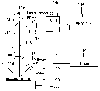
[0011] Fig. 1 schematically represents an apparatus according to one
embodiment
of the disclosure;
[0012] .Fig. 2 schematically represent an apparatus according to another
embodiment of the disclosure;
[0013] Fig. 3 shows Raman image of a sample using a method and apparatus in
accordance with one embodiment of the disclosure; and
[0014] Fig. 4 shows a Raman spectrum extracted from the hyperspectral image of
polyethylene naphthalate shown in Fig. 4.
Detailed Description of the Disclosure
[0015] The various embodiments of the disclosure provide low cost optical
device
and methods particularly suited for spectral imaging systems by providing
higher light
delivery in conjunction with high collection efficiency and reduced scattering
of the
resolutions of imaging applications. Conventional lens objectives are more
complex and
costly than the apparatus disclosed according to the principles disclosed
herein. Since the
4

CA 02571473 2006-12-21
WO 2006/007065 PCT/US2005/016142
color and the resolution of the viewed sample is determined by the tunable
filter and the
resolution of the imaging detector, the system need not use a conventional
high
resolution, low aberration lens as used in conventional microscopes. Indeed, a
simpler
reduced resolution/aberration lens can be designed with larger numeral
aperture to
increase system throughput (light delivery and collection efficiency) while
providing the
same quality resolution as the conventional systems.
[0016] The radiation used to illuminate the sample need not pass through the
optical train of a conventional microscope or macroscope. It can be
illuminated from the
underside of the sample. This results in reduced internal scattering and
attenuation of the
incident exciting photons. The location of the illumination source external to
the optical
train further enables a simpler, low power / low cost illumination sources as
well as a
lower cost of integration of several illumination sources into one system.
[0017] In micro-Raman spectroscopy, for example, the illuminating beam and the
microscope are focused on a diffraction-limited spot for collecting the Raman
scattered
light. The same imaging system is also used in full field-of-view Raman
imaging. Such
instrument configuration has proved optically inefficient and costly. The
combined
optical losses due to laser light delivery and Raman scattered light
collection can severely
limit the number of Raman chemical imaging applications. Optical inefficiency
occurs
because much of the optical signal of interest must be spectrally separated
from the
incident laser light as the latter is many orders of magnitude more intense
than the Raman
scattered light. Consequently, the detected Raman signal is dramatically
reduced because
it must be spectrally and angularly resolved.
[0018] Fig. 1 schematically represents an apparatus according to one
embodiment
of the disclosure. The apparatus of Fig. 1 enables providing a high optical
throughput for
imaging low light levels at variable magnification. Referring to Fig. 1,
sample 100 is

CA 02571473 2006-12-21
WO 2006/007065 PCT/US2005/016142
positioned on substrate 105. Substrate 105 can be any conventional microscopic
slide or
other means for receiving and optionally securing sample 100.
[0019] Light source 110 is positioned to provide incident light to sample 100.
Light source 110 can include any conventional photon source, including laser,
LED, and
other IR or near IR devices. Light source 110 may also be selected to provide
evanescence illumination of the sample. In one embodiment, the wavelength of
the
source is in the range of about 15-25 cm 1. Referring to Fig. 1, it should be
noted that
light source 110 is positioned to provide incident light at. an -angle to
sample 100 as
opposed to light shining orthogonal to sample 100. In other words, the
radiation used to
illuminate the sample need not pass through the optical train of a
conventional
microscope (or macroscope); rather, it can illuminate the sample at an oblique
angle from
above or below sample 100. Photon beam 112 is received and deflected by mirror
115
through lens 120. Lens 120 may optionally be used to focus the light on sample
100.
Alternatively, the photon beam 112 may be directed towards the sample 100
without the
need for the mirror 115.
[0020] The multitude of photons in beam 112 reaching sample 100 are absorbed
by
the sample or scatter upon reaching the sample. Scattered photons are
schematically
represented as beams 116 and 118 while spectrally reflected photons are
represented
schematically as beam 114. Luminescence emitted photons are also represented
as beam
118. Optical lens 125 is positioned to receive emitted and scattered photon
beams 116
and 118. The term 'luminescence' has been conventionally used to include a
wide range
of optical processes including fluorescence, phosoporescence,
photoluminescence,
electroluminescence, chemiluminescence, sonoluminescence, thermoluminescence
and
even upconversion. Optical lens 125 may be used for gathering and focusing
received
photon beams. This includes gathering and focusing both polarized and the un-
polarized
photons. In general, the sample size determines the choice of light gathering
optical lens
125. For example, a microscope lens may be employed for analysis of the sub-
micron to
6

CA 02571473 2006-12-21
WO 2006/007065 PCT/US2005/016142
micrometer specimens. For larger samples, macro lenses can be used. Optical
lens 125
(as well as lens 120) may include simple reduced resolution/aberration lens
with larger
numerical aperture to thereby increase system's optical throughput and
efficiency.
[0021] Mirror 130 is positioned to direct emitted or scattered photon beams
118 to
tunable filter 140. It should be noted that placement of mirror 130 is
optional and may be
unnecessary in configurations where tunable filter is positioined above sample
100.
[0022] Laser rejection filter 135 may be positioned prior to tunable filter
140 to
filter out scattered illumination light represented by beam 116 and to
optimize the
performance of the system. In other words, rejection filter 135 enables
spectral filtering
of light at the illuminating wavelength. For optimal performance, a computer
may be
used to control any of the optical devices shown in Fig. 1 including the
lenses (120, 125,
135), mirrors (1.15, 130) and the tunable filter 140.
[0023] A conventional tunable filter (including electro-optical tunable
filters)
including liquid crystal tunable filter ("LCTF") or acousto-optical tunable
filter
("AOTF") can be used to further the principles of the disclosure. The electro-
optical
filters (interchangeably, tunable filters) allow specific wavelengths or
ranges of
wavelengths of light to pass through as an image, depending on the control
signals placed
on the device by a controller (not shown). The wavelengths that can be passed
through
tunable filter 140 may range from 200 nm (ultraviolet) to 2000 nm (i.e., the
far infrared).
The choice of wavelength depends on the desired optical region and/or the
nature of the
sample being analyzed.
[0024] Image sensor 145 may be a digital device such as a two-dimensional,
image
focal plane array ("FPA"). The optical region employed to characterize the
sample of
interest governs the choice of FPA detector. For example, silicon charge-
coupled device
("CCD") detectors, can be employed with visible wavelength fluorescence and
Raman
spectroscopic imaging, while gallium arsenide (GaAs) and gallium indium
arsenide
7

CA 02571473 2006-12-21
WO 2006/007065 PCT/US2005/016142
(GaInAs) FPA detectors can be employed for image analyses at near infrared
wavelengths. The choice of such devices depends on the type of sample being
analyzed.
Image sensor 145 produces digital images of the entire view of the sample as
processed
by tunable filter 140.
[0025] Fig. 2 schematically represents an apparatus according to another
embodiment of the disclosure. More specifically, Fig. 2 schematically shows a
high
optical throughput configuration for imaging low light levels at variable
magnification.
The collection optics are similar to that illustrated in Fig. 1 but with
illumination from the
underside of sample 100.
[0026] It is noted that in both Figs. 1 and 2, sample 100 is illuminated at an
oblique
angle. Specifically referring to Fig. 2, photonic beam 120 and the plane axis
of sample
100 define an oblique angle. It has been found that through oblique
illumination, a so-
called "Dark Field Raman Imaging" is developed. As opposed to the conventional
bright
field Raman configuration, the dark field Raman imaging decouples the image
capture
optics from the deliver of exciting radiation. Consequently, internal
scattering and
attenuation of the incident radiation has been minimized. Also, the location
of the optical
source external to the optical train further enables a simpler, less expensive
integration of
several illumination sources into the system. The application of this
configuration is, not
limited to Raman and luminescence imaging and can be successfully used, for
example,
with conventional spectroscopy.
[0027] The configuration disclosed herein is particularly suitable for Raman
imaging of micro fluid circuits or biological samples undergoing change. These
changes
may include displacement, chemical interaction, a change in chemical state,
phase
change, growth, shrinkage, chemical decomposition, chemical metabolization and
physical strain.
8

CA 02571473 2006-12-21
WO 2006/007065 PCT/US2005/016142
[0028] Fig. 3 shows Raman image of a sample using a method and apparatus in
accordance with one embodiment of the disclosure. More specifically, Fig. 3
shows
Raman image of a polyethylene naphthalate pellet at 1389 cm 1 obtained with
single lens
imaging apparatus according to an embodiment of the disclosure. The incident
power
was about 100 mW of 532 nm light illuminated over a circular region 3 mm in
diameter.
The image was captured using a 512 X 512 CCD integrated for 2.0 Sec with 2X2
binning. Fig. 4 shows a Raman spectrum extracted from the hyperspectral image
of
polyethylene napthalate shown in Fig. 4. The Raman spectrum shown in Fig. 4 is
substantially free from optical noise prevalent wlien using a
conventional'testing
configuration.
[0029] Although the principles disclosed herein have been described in
relation
with the non-exclusive exemplary embodiments provided herein, it should be
noted that
the principles of the disclosure are not limited thereto and include
permutations and
variations not specifically described.
9

Dessin représentatif
Une figure unique qui représente un dessin illustrant l'invention.
États administratifs

2024-08-01 : Dans le cadre de la transition vers les Brevets de nouvelle génération (BNG), la base de données sur les brevets canadiens (BDBC) contient désormais un Historique d'événement plus détaillé, qui reproduit le Journal des événements de notre nouvelle solution interne.

Veuillez noter que les événements débutant par « Inactive : » se réfèrent à des événements qui ne sont plus utilisés dans notre nouvelle solution interne.

Pour une meilleure compréhension de l'état de la demande ou brevet qui figure sur cette page, la rubrique Mise en garde , et les descriptions de Brevet , Historique d'événement , Taxes périodiques et Historique des paiements devraient être consultées.

Historique d'événement

Description Date
Demande non rétablie avant l'échéance 2010-05-06
Le délai pour l'annulation est expiré 2010-05-06
Inactive : Abandon. - Aucune rép dem par.30(2) Règles 2009-08-24
Réputée abandonnée - omission de répondre à un avis sur les taxes pour le maintien en état 2009-05-06
Inactive : Dem. de l'examinateur par.30(2) Règles 2009-02-24
Inactive : IPRP reçu 2008-02-15
Lettre envoyée 2008-02-13
Inactive : Transfert individuel 2007-12-21
Lettre envoyée 2007-03-29
Requête d'examen reçue 2007-03-14
Exigences pour une requête d'examen - jugée conforme 2007-03-14
Toutes les exigences pour l'examen - jugée conforme 2007-03-14
Inactive : Page couverture publiée 2007-02-27
Inactive : Lettre de courtoisie - Preuve 2007-02-27
Inactive : Notice - Entrée phase nat. - Pas de RE 2007-02-21
Demande reçue - PCT 2007-01-23
Exigences pour l'entrée dans la phase nationale - jugée conforme 2006-12-21
Demande publiée (accessible au public) 2006-01-19

Historique d'abandonnement

Date d'abandonnement Raison Date de rétablissement
2009-05-06

Taxes périodiques

Le dernier paiement a été reçu le 2008-05-06

Avis : Si le paiement en totalité n'a pas été reçu au plus tard à la date indiquée, une taxe supplémentaire peut être imposée, soit une des taxes suivantes :

  • taxe de rétablissement ;
  • taxe pour paiement en souffrance ; ou
  • taxe additionnelle pour le renversement d'une péremption réputée.

Les taxes sur les brevets sont ajustées au 1er janvier de chaque année. Les montants ci-dessus sont les montants actuels s'ils sont reçus au plus tard le 31 décembre de l'année en cours.
Veuillez vous référer à la page web des taxes sur les brevets de l'OPIC pour voir tous les montants actuels des taxes.

Historique des taxes

Type de taxes Anniversaire Échéance Date payée
Taxe nationale de base - générale 2006-12-21
TM (demande, 2e anniv.) - générale 02 2007-05-07 2007-03-14
Requête d'examen - générale 2007-03-14
Enregistrement d'un document 2007-12-21
TM (demande, 3e anniv.) - générale 03 2008-05-06 2008-05-06
Titulaires au dossier

Les titulaires actuels et antérieures au dossier sont affichés en ordre alphabétique.

Titulaires actuels au dossier
CHEMIMAGE CORPORATION
Titulaires antérieures au dossier
DAVID TUSCHEL
MYLES P. BERKMAN
WESLEY H. HUTCHISON
Les propriétaires antérieurs qui ne figurent pas dans la liste des « Propriétaires au dossier » apparaîtront dans d'autres documents au dossier.
Documents

Pour visionner les fichiers sélectionnés, entrer le code reCAPTCHA :


Pour visualiser une image, cliquer sur un lien dans la colonne description du document. Pour télécharger l'image (les images), cliquer l'une ou plusieurs cases à cocher dans la première colonne et ensuite cliquer sur le bouton "Télécharger sélection en format PDF (archive Zip)" ou le bouton "Télécharger sélection (en un fichier PDF fusionné)".

Liste des documents de brevet publiés et non publiés sur la BDBC .

Si vous avez des difficultés à accéder au contenu, veuillez communiquer avec le Centre de services à la clientèle au 1-866-997-1936, ou envoyer un courriel au Centre de service à la clientèle de l'OPIC.


Description du
Document 
Date
(aaaa-mm-jj) 
Nombre de pages   Taille de l'image (Ko) 
Revendications 2006-12-20 13 441
Abrégé 2006-12-20 1 60
Description 2006-12-20 9 474
Dessins 2006-12-20 3 104
Dessin représentatif 2007-02-25 1 7
Accusé de réception de la requête d'examen 2007-03-28 1 176
Rappel de taxe de maintien due 2007-02-20 1 110
Avis d'entree dans la phase nationale 2007-02-20 1 192
Courtoisie - Certificat d'enregistrement (document(s) connexe(s)) 2008-02-12 1 108
Courtoisie - Lettre d'abandon (taxe de maintien en état) 2009-07-01 1 172
Courtoisie - Lettre d'abandon (R30(2)) 2009-11-15 1 163
PCT 2006-12-20 1 23
Correspondance 2007-02-20 1 27
Taxes 2007-03-13 1 35
PCT 2006-12-21 5 274