Note : Les descriptions sont présentées dans la langue officielle dans laquelle elles ont été soumises.
CA 02573900 2007-01-15
BACKGROUND OF THE INVENTION
1 1. Field of the Invention:
2
3 The present invention generally relates portable lighting apparatus and,
more particularly,
4 to optical, mechanical, and electrical features for the design, utility, and
performance of portable task
lighting and flash light apparatus using very small light emitting devices.
6
7 2. Description of the Prior Art:
8
9 Lighting devices can be grouped into two basic applications: illumination
devices and
signaling devices. Illumination devices enable one to see into darkened areas.
Signaling devices are
11 designed to be seen, to convey information, in both darkened and well-lit
areas. Widely available
12 varieties of portable lighting apparatus, which may combine both the
illumination type and the
13 signaling type, employ a variety of lighting technologies in products such
as task lamps and
14 flashlights. Each new development in technology is followed by products
that attempt to take
advantage of the technology to improve performance or provide a lower cost
product. For example,
16 incandescent bulb technology in small and/or portable lighting products is
being challenged by
17 compact fluorescent lamp (CFL) bulbs, often in association with electronic
ballast circuits. Other
18 types of incandescent bulbs such as halogen lamps have become standard in a
number of ordinary
19 applications. High intensity discharge (HID) and other arc lighting
technologies are finding ready
markets in automotive and high brightness flood lighting, spot lighting, and
signaling applications.
21
22 More recently, solid state or semiconductor devices such as light emitting
diodes are finding
23 use as compact and efficient light sources in a wide variety of
applications. These applications
24 include high intensity personal lighting, traffic and other types of signal
lighting, automotive tail
lamps, bicycle lighting, task lighting, flashlights, etc., to name a few
examples. This technology is
26 relatively new, however, and conventional products heretofore have suffered
from a number of
27 deficiencies. For example, current products utilizing light emitting diodes
as light sources tend to
-2-
CA 02573900 2007-01-15
1 be highly specialized and suited to only a single use, thus limiting their
versatility as lighting devices
2 or instruments for more ordinary uses. Further, such specialized devices
tend to be expensive
3 because of the relatively low production volumes associated with specialized
applications.
4
Moreover, there exist certain lighting applications for which conventional
light sources are
6 unsatisfactory because of limitations in brightness, operating life,
durability, power requirements,
7 excessive physical size, poor energy efficiency, and the like. Newer light
sources such as
8 semiconductor light emitting diodes are very small, very durable, use
relatively little power, have
9 long lifetimes, and emit very bright light relative to the electrical power
input. While some presently
available products employ these semiconductor light sources, their full
potential is frequently not
11 realized. This may occur because of deficiencies in optical components and
drive circuits, or
12 interface components having particular combinations of structure and
function are not available.
13 Another factor may be that improvements in the design and configuration of
multiple, small, high
14 intensity light sources for maximum illumination efficiency and convenience
of use have not been
forthcoming.
16
17 An advance in the state of the art could be realized if such small, high
intensity and high
18 efficiency light emitting devices could be adapted to more general and more
versatile lighting
19 applications such as flood lighting or spot lighting. Such advances could
occur if improvements in
the components, circuits, and product architecture are developed and provided.
21
22 For example, in the field of lighting devices used by security personnel,
there is a need for
23 high intensity illumination in a battery powered, hand-held instrument that
is very rugged, efficient
24 in the use of power, and that provides a beam of light designed to
illuminate dark regions of or
indistinct objects within an areabeing patrolled or investigated. Many
circumstances require abright,
26 well-shaped flood light beam for illuminating relatively large areas. Other
situations require a more
27 directed beam of light, to spotlight particular areas or objects. Ideally,
both modes of illumination
28 would be combined in a single instrument.
29
-3-
CA 02573900 2007-01-15
1 SUMMARY OF THE INVENTION
2
3 Accordingly, in one aspect of the present invention, there is provided a
combination task
4 lamp and flash light, comprising first and second elongated shells forming
an elongated, tubular
housing having a longitudinal axis, a first section at a first end for
containing a plurality of light
6 emitting device (LED) light sources and a second section at a second end for
containing a power
7 supply; the first section of the combination including a first directed
array of LED/lens assemblies
8 for providing flood light illumination and a second directed light array of
at least one LED/lens
9 assembly for providing spot light illumination.
11 In another aspect of the invention, there is provided a lens for a light
emitting device (LED)
12 comprising a combination of an aspherical reflecting surface and a
spherical refracting surface. The
13 aspherical reflecting surface has a focal point and a central axis of
symmetry - i.e., an optical axis
14 - for reflecting light rays emitted from a compact light source located
approximately at the focal
point in a forward direction and the reflected light rays are emitted
approximately within a
16 predetermined angle with respect to the optical axis. The spherical
refracting surface is disposed in
17 the path of the reflected light rays, centered on and normal to the central
axis, concave in the forward
18 direction of the reflected light rays and joins the aspherical reflecting
surface at a boundary
19 equidistant from the optical axis. The spherical refracting surface
includes a plurality ofN concentric
annular surfaces, each annular surface having a cross section convex in the
forward direction and
21 disposed substantially at uniform radial intervals between the optical axis
and the junction with the
22 aspherical reflecting surface.
23
24 In another aspect of the present invention, there is provided a circuit for
illuminating multiple
light emitting devices, comprising a current selector circuit connected across
a positive terminal and
26 a negative terminal of a DC supply for selecting operating current from the
DC supply to each of a
27 first array and a second array of the multiple light emitting devices
(LEDs); a switching regulator
28 circuit connected across an output of the current selector circuit for
respectively regulating first and
29 second constant drive currents to the first array of LEDs and to the second
array of LEDs; a first
-4-
CA 02573900 2007-01-15
1 array of LEDs coupled between a first output of the switching regulator
circuit and a common current
2 sense device; and a second array of LEDs coupled between the first output of
the switching regulator
3 circuit and the common current sense device; wherein a voltage signal
generated by the common
4 current sense device is coupled to a sense input of the switching regulator
circuit for regulating the
constant drive currents supplied to the first and second arrays of LEDs.
6
7 In another aspect of the invention, there is provided a light emitting
module comprising a
8 frame configured as a heat sink having first and second opposite sides and a
forward axis normal to
9 the first side thereof. Each one of an array of a plurality N of light
emitting assemblies (LEAs)
connected to a source of current is mounted on the first side of the frame
configured as a heat sink
11 such that the central axis of light emission of each LEA is disposed at a
non-zero first predetermined
12 angle relative to the forward axis. The frame may include a printed circuit
embodying an electric
13 circuit coupled to the array of light emitting assemblies.
14
In yet another aspect of the present invention, there is provided an electric
circuit comprising
16 an electric circuit having an output and a single pole, single throw (SPST)
switch having normally
17 open (NO) first and second contacts and a latching mechanism operable by an
actuating member.
18 The switch is connected in the electric circuit for activating at least a
conducting path in the electric
19 circuit wherein the switch is sequentially operable in first, second, and
third states corresponding
respectively to latched engagement, momentary disengagement, and latched
disengagement of the
21 first and second contacts in the switch. The first state provides
activation of the electric circuit in an
22 OFF condition, the second state provides momentary activation of the
electric circuit in an ON
23 condition, and the third state provides latched activation of the electric
circuit in an ON condition.
24
In yet another aspect of the present invention, there is provided a method of
operating a single
26 pole, single throw (SPST) switch in three distinct states in an electric
circuit. The method comprises
27 the steps of providing in an electric circuit having at least an output a
SPST normally open (NO)
28 switch for activating at least a conducting path in the electric circuit,
the switch having first and
29 second contacts and a latching mechanism operated by an actuating member;
providing a first state
-5-
CA 02573900 2007-01-15
I wherein the latching mechanism is activated, the first and second contacts
are engaged, and the
2 electric circuit is in an OFF condition; providing a second, momentary state
by exerting a first force
3 upon the actuating member of the SPST switch, sufficient to disengage but
not latch the first and
4 second contacts, thereby causing the electric circuit to enter a temporary
ON condition during the
second state, wherein release of the first force upon the actuating member
causes restoration of the
6 first state; and providing a third state by exerting a second force greater
than the first force upon the
7 actuating member of the SPST switch, wherein the latching mechanism is
activated and the first and
8 second contacts are disengaged, causing the electric circuit to remain in an
ON condition. A repeated
9 exertion of the second force upon the actuating member of the SPST switch
causes engagement of
the first and second contacts, causing in turn the electric circuit to enter
the OFF condition.
11
-6-
CA 02573900 2007-01-15
1 BRIEF DESCRIPTION OF THE DRAWINGS
2
3 The foregoing aspects and other objects of the invention disclosed herein
will be understood
4 from the following detailed description read with reference to the
accompanying drawings of one
embodiment of the invention. Structures appearing in more than one figure and
bearing the same
6 reference number are to be construed as the same structure.
7
8 Figure 1 illustrates one embodiment of a perspective view of a combination
task lamp and
9 flash light according to the present invention that provides both flood and
spot light illumination;
11 Figure 2 illustrates a perspective view of the embodiment of Figure 1
showing a preferred
12 configuration of light emitting assemblies and the directionality of their
respective emissions of light;
13
14 Figure 3 illustrates a plan view of a flood light pattern on a flat target
surface at a nominal
distance from the embodiment of Figure 1, showing the overlapping of beams of
light from
16 individual emitters;
17
18 Figure 4A illustrates a cross section profile of a solid body lens for use
with each light
19 emitting device in the embodiment of Figure 1;
21 Figure 4B illustrates an enlarged cross section of a portion of Figure 4A
to show detail
22 thereof;
23
24 Figure 4C illustrates a cross section profile of the solid body lens of
Figure 4A in assembly
with a light emitting device assembly;
26
27 Figure 5 illustrates a block diagram of an electrical circuit for use in
the embodiment of
28 Figure 1 for powering and controlling the light outputs thereof;
29
-7-
CA 02573900 2007-01-15
1 Figure 6A illustrates a first portion of a schematic diagram of the
electrical circuit of Figure
2 5;
3
4 Figure 6B illustrates a second portion of the schematic diagram of the
electrical circuit of
Figure 5;
6
7 Figure 7 illustrates an exploded view of major parts and assemblies of the
embodiment of
8 Figure 1;
9
Figure 8A illustrates a perspective view of a rearward side of a light
emitting module of the
11 embodiment of Figure 1;
12
13 Figure 8B illustrates a perspective view of the forward side of the light
emitting module
14 illustrated in Figure 8A;
16 Figure 8C illustrates a perspective view of a basic module portion of the
light emitting
17 module appearing in Figure 8B; and
18
19 Figure 8D illustrates a side cross section view of the light emitting
module of the
embodiment of Figure 8A and 8B.
-8-
CA 02573900 2007-01-15
1 DETAILED DESCRIPTION OF THE INVENTION
2
3 Referring to Figure 1, there is illustrated one embodiment of a perspective
view of a portable,
4 combination task lamp and flash light (also referred to herein as a portable
lighting device 10 or
"PLD 10," that provides both flood and spot light illumination, and is
constructed according to the
6 present invention. The PLD 10 includes an elongated tubular housing 12
defined along a longitudinal
7 axis 14, having a first section 16 at a first end for containing a plurality
of light emitting assemblies
8 or light sources 22, and further having a second section 18 at a second end
for containing a power
9 supply (See Figure 7). Visible through a clear side lens 24 in Figure 1 is a
beze120 that locates the
forward surfaces of four light sources 22 substantially in a row. The side
lens 24 is an internal
11 component of the housing 12 as will be further described with Figure 7. The
row of four light
12 sources 22 may be denoted as a first directed array of light sources 22.
Any number of individual
13 light sources 22 maybe arranged in a variety of configurations to form a
directed array. In the present
14 illustrative embodiment, the configuration of four light sources 22
disposed in a row is selected to
illustrate the principles of the invention in a specific product application.
16
17 In general, each of the light sources 22 may be a combination of a light
emitting device
18 (LED) and a lens assembly. The combination of an LED and a lens assembly
may further be denoted
19 as a light emitting assembly (LEA) or as a lens/LED assembly. An LED may be
a semiconductor
light emitting diode or it maybe a light emitting device employing a different
technology to produce
21 light. A lens assembly may be a single, solid body of optical material
having one or more
22 predetermined optically responsive surface configurations or it maybe
constructed as a combination
23 of separate, predetermined optical elements assembled into a single unit.
In the illustrated
24 embodiment, the lens is a solid body element having a plurality of
predetermined surface
configurations that is designed for use with certain types of light emitting
diodes.
26
27 Continuing with Figure 1, a clear top lens 28 of a second directed light
array 26 is disposed
28 in the end of the first section 16 of the elongated housing 12. Although
the clear top lens 28
29 indicates that a single light source is shown in the illustrative
embodiment, it is possible that several
-9-
CA 02573900 2007-01-15
1 individual light sources may be used to construct the second directed light
array 26. The second
2 directed light array 26 visible through the clear top lens 28 may be
configured as a spot light beam
3 or as a flood light beam. Typically, with a PLD 10 having a first directed
light array 22 configured
4 to provide a flood light beam, the second directed light array 26 may be
advantageously configured
as a spot light beam. As will become apparent, when using very small or
compact light sources, the
6 type of light beam provided is largely dependent upon the lens assembly
provided for the light
7 source. Generally, the light source for the second directed light array 26
may be aligned such that its
8 optical axis is coincident with or aligned parallel with the longitudinal
axis 14. In other applications,
9 the alignment of the second directed array 26 may be disposed at an angle
(fixed or adjustable)
relative to the longitudinal axis. In such cases, the optical axis of the
second directed light array 26
11 would be aligned at a non-zero angle with respect to the longitudinal axis.
12
13 At the end of the first section 16 of the elongated housing 12 a lens frame
30 disposed over
14 the second directed light array of lens 26 is provided to protect the clear
top lens 28. The lens frame
30 may be formed as part of the elongated housing 12 or implemented as a
separate component. It
16 will be observed that the lens frame 30 has a three-sided, tubular shape,
i.e., a substantially triangular
17 shape wherein the three sides bulge slightly outward as with a convex
surface. This triangular shape
18 mimics the shape of the cross section of the elongated housing 12 in the
first section 16. In the
19 illustrated embodiment, the triangular cross section of the first section
16 may be configured to
merge with a substantially round or oval cross section of the second section
18. The triangular shape
21 is provided so that when the PLD 10 is placed on a horizontal surface, the
PLD 10 naturally assumes
22 an orientation so that the flood light beam from the first directed light
array is projected upward at
23 an angle from the horizontal. This is a useful feature when both hands must
be free to work.
24
At the opposite end of the elongated housing 12, the second section 18 may be
configured
26 to contain a power supply such as a battery pack. The external portions of
the second section 18 may
27 be formed as a handle or with other features to provide a comfortable or a
non-slippery gripping
28 surface. A removable end cap 32 may be provided for access to the interior
of the second section 18
29 of the elongated housing 12 such as to replace a battery. In other
applications the cap 32 may include
-10-
CA 02573900 2007-01-15
1 a connector for a line cord (not shown in Figure 1) to supply external power
to a power supply
2 converter or battery charger contained within the second section 18, for
example.
3
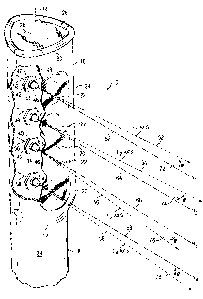
4 Referring to Figure 2, there is illustrated a perspective view of the
embodiment of Figure 1
showing a preferred configuration of light emitting assemblies and the
directionality of their
6 respective emissions of light. As will be described further with Figures 4A,
4B, and 4C infra, each
7 of the light sources 22 is an assembly of a light emitting assembly
(including a light emitter or light
8 emitting device) and a lens assembly. In Figure 2, each of the light sources
22 is shown aligned with
9 respect to an associated light emitter (designated as E1, E2, E3, and E4)
along an optical axis thereof.
The light emitting assembly including the light emitter and the lens assembly
share the same optical
11 axis. In the example illustrated in Figure 2, the optical axis (designated
by a dashed line) of the light
12 emitter of each light source 22 is disposed at an angle 0 with respect to a
normal reference line
13 (designated as N1, N2, N3, and N4) at the location of each light source 22.
It is known to persons
14 skilled in the art that a"normal" reference line is oriented perpendicular
to a plane surface, in this
case to the plane surface 48 on which the focal point of the individual light
emitter is located. The
16 angle 0 will be described in further detail herein below.
17
18 Each of the light emitters E1, E2, E3, and E4 are shown mounted on the
plane surface 48 in
19 the interior of the elongated housing 12. The light sources 22, associated
with each of the light
emitters are not fully illustrated so that the relationship of the light
emitters E1, E2, E3, and E4 and
21 the elongated housing 12 may be more clearly illustrated. In the
illustrated embodiment, a light
22 emitter may be a light emitting diode having an active element (See also
Figure 4C) mounted inside
23 a hemispherical dome 40 on a base 42. The base 42 may be attached to a
substrate 44, such as a
24 printed circuit board. The substrate 44 may be a laminated structure that
includes a bottom layer (not
shown) of thermally conductive material such as aluminum. The aluminum layer
provides an integral
26 heat sink for the light source emitter assembly for low power applications
and a suitable conductive
27 bonding surface for higher power applications where more heat must be
dissipated via an external
28 heat sink in contact with the substrate 44. In the illustrated example, the
plane surface 48 is
29 preferably configured as such external heat sink for conducting heat away
from the light emitting
-11-
CA 02573900 2007-01-15
1 assembly and dissipating it into the surroundings. A thermal compound of the
type well known in
2 the art may be placed in the interface between the substrate 44 and the
plane surface 48.
3
4 As described previously, an optical axis is defined for each of the light
sources 22. In the
illustrated embodiment, the optical axes are defined at an angle 0 with
respect to the normal line
6 defined for each of the light sources 22. The same angle 0 is used in this
particular embodiment for
7 all four of the light emitting assemblies for reasons which will be
described. Thus, the optical axis
8 52 for the E1 emitter is shown by the dashed line labeled "E1 Axis" and
bearing reference number
9 52. Optical axis 52 is defined to be oriented vertically upward relative to
the normal line 62 (N1),
from the perspective of the PLD 10, at the angle indicated by the symbol 0.
Similarly, optical axis
11 54 (the E2 axis) is defined to be oriented horizontally leftward relative
to the normal line 64 (N2),
12 from the perspective of the PLD 10, at the angle indicated by the symbol 0.
Similarly, optical axis
13 56 (the E3 axis) is defined to be oriented horizontally rightward relative
to the normal line 66 (N3),
14 from the perspective of the PLD 10, at the angle indicated by the symbol 0.
Likewise, optical axis
58 (the E4 axis) is defined to be oriented vertically downward relative to the
normal line 68 (N4),
16 from the perspective of the PLD 10, at the angle indicated by the symbol 0.
Thus, each of the light
17 sources 22 is oriented or aimed at the angle 6 relative to a normal
reference line perpendicular to the
18 plane surface 48 at the location of the particular light source 22.
19
Moreover, in an array of N light emitting assemblies supported on a common
planar base
21 having a normal forward axis, the individual optical axes of the light
emitting assemblies will be
22 disposed such that they diverge from a reference line parallel to the
forward axis by the angle 0.
23 Further, the individual planes containing the reference line and the
optical axis of each light emitting
24 assembly are disposed at substantially equal angles from each other, in the
manner of spokes of a
wheel when viewed from a point on the forward axis looking back toward the
origin of the forward
26 axis. This arrangement of the optical axes of the individual light emitting
assemblies is shown in
27 Figure 2 for an array of N = 4 emitters arranged in a straight line on a
flat common planar base. As
28 will be described, the orientation of the optical axes of this array at the
angle 0 of approximately 5
29 degrees (5 ), wherein each light emitting assembly provides a beam of light
having a beam width
-12-
CA 02573900 2007-01-15
1 angle of approximately40 degrees (40 ), a compositebeam pattern ofhigh
brightness and uniformity
2 of cross section is provided.
3
4 It should be appreciated that the optical axes of opposing pairs of light
emitting assemblies
in such an array diverge by twice the angle 0, which in the illustrated
embodiment is 2 X 5 = 10 .
6 During the development of the present invention, it was discovered that the
relationship between the
7 amount of divergence between two light emitting assemblies in an array (here
10 ) and the beam
8 width angle of the individual light emitting assemblies in the array (here
40 ) turns out to be an
9 optimum relationship for producing a high brightness, high uniformity
composite beam cross section.
The relationship may be stated as the ratio of the divergence angle to the
beam width angle. In this
11 example it is one to four, or a "one quarter beam width" index or figure of
merit. Thus, for a given
12 beam width from a light emitting assembly having a substantially point
source light emitter and a
13 lens assembly configured to produce the given beam width, the optimum
amount of divergence
14 between two such light emitting assemblies or pairs of such light emitting
assemblies turns out to
be one quarter of the beam width of the individual light emitting assemblies.
This index is very
16 useful in devising arrays of light emitting assemblies to provide a
particular composite beam of light
17 or illumination pattern from the array, as will become more apparent in the
detailed description
18 which follows.
19
Continuing with the description of Figure 2, when the plane surface 48 is a
flat surface, all
21 four of the normal lines at each of the light source positions are parallel
to each other. In the
22 illustrated embodiment, the light sources are disposed in a row because of
the space limitations of
23 the elongated tubular housing 12. However, in an embodiment that allowed
the four light sources
24 to be clustered close together on a flat plane surface in a rectangular
array, for example at the four
corners of a square, the normal lines may be closer together and, in fact, a
single normal line placed
26 at the center of the array could serve as the reference for all four of the
light sources. In such an
27 embodiment, the light sources would still be advantageously oriented with
their optical axes
28 diverging from the common normal line by the angle 0. Further, each of the
four light sources would
29 also be divergent in a direction that is at right angles from the direction
of divergence of each of its
-13-
CA 02573900 2007-01-15
1 neighboring light source. Thus, the optical axes - and the respective light
beams - of the four light
2 sources are aimed in a manner that mimics the four compass directions N, W,
S, and E, or, the four
3 spokes of a wheel wherein the spokes are 90 apart.
4
The same aiming arrangement is provided in the illustrated embodiment of
Figure 2, where
6 the four light sources 22 are arranged in a row. That is, the optical axes
of the light sources 22
7 diverge in the compass directions N, W, S, and E, when viewed from the
position of the longitudinal
8 axis 14, even though the light sources 22 are arranged in a single row and
are somewhat more widely
9 spaced. In either of the described embodiments, as illustrated in Figure 2
or in the preceding
paragraph, from the perspective of the PLD 10, the beam from light source E 1
diverges northward,
11 E2 diverges westward, E3 diverges southward, and E4 diverges eastward.
Thus, the respective beam
12 cross sections, as the composite beam is projected on a flat wall surface,
will include some overlap.
13 This characteristic will be shown in Figure 3 to be described.
14
In the illustrative embodiment, the angle 0 is a non-zero angle typically less
than
16 approximately ten degrees (10 ). In the preferred embodiment, 0 is
approximately 5 . This amount
17 of divergence provides an enhanced flood light pattern when projected on a
plane surface at a
18 distance of three to four meters, as shown in Figure 3, to be described.
Experimentation has shown
19 that the angle 0 is dependent on the design of the lens assembly,
particularly the factors of the lens
assembly that affect the angle (3 of the beam width. The beam width angle (3
is the angle between
21 the sides of a cone that defines the locus of the light rays emitted from a
light source located at the
22 apex of the cone. Further, as described herein above, the beam width angle
P, the optical axis
23 divergence angle 0, and the properties and positions of the aspherical
surfaces of the lens assembly
24 may be adjusted according to the one quarter beam width index to produce
the brightest, most
uniform flood light pattern at a distance of three to four meters in the
illustrative embodiment. The
26 relationships of these parameters will become clearer in the description
which follows.
27
28 In some embodiments, the plane surface 48 shown in Figure 2 may be curved
to provide a
29 particular orientation of the light emitting assemblies mounted thereon.
Thus, with the focal points
-14-
CA 02573900 2007-01-15
1 of the light emitting assemblies coincident with the plane surface 48,
bending the plane surface to
2 provide a predetermined curvorients the optical axes of the individual light
emitting assemblies to
3 conform to other beam configurations. In such cases the forward axes may be
defined at the location
4 of each of the light emitting assemblies. Further, the optical axes of the
individual light emitting
assemblies may be oriented at non-zero or zero angles with respect to the
reference forward axis at
6 a particular location on the plane surface 48. In yet other embodiments the
curvature or departure
7 from flat of the plane surface 48 may be adjustable, either in production or
by the user, to produce
8 several beam outputs adapted to different applications. In the example
described above, bending the
9 plane surface 48 is by way of illustration and not intended to limit the
choice of design or method
available to the designer. Other design configurations may of course be
implemented to configure
11 the mounting surface for the light emitting assemblies with the desired
curvature.
12
13 Referring to Figure 3, there is illustrated a plan view of an overall flood
light pattern
14 projected on a flat target surface at a nominal distance from the
embodiment of Figure 1, showing
the overlapping of beams of light from individual emitters to form a composite
beam 80. Figure 3
16 will be best understood when viewed in combination with Figure 2. Each of
the regions identified
17 in Figure 3 are distinguished by the relative amount of shading applied to
the various regions. Thus,
18 light emitter El having an optical axis 52 provides a projected beam cross
section or pattern 82.
19 Similarly, light emitter E2 having an optical axis 54 provides a projected
beam cross section or
pattern 84. Similarly, light emitter E3 having an optical axis 56 provides a
projected beam cross
21 section or pattern 86. Likewise, light emitter E4 having an optical axis 58
provides a projected beam
22 cross section or pattern 88.
23
24 Continuing with Figure 3, the result of combining the respective patterns
82, 84, 86, and 88
produces the overlap region 90 in the center portion of the composite beam 80,
where all four of the
26 beams overlap. In this central region 90, the pattern resembles a square
with rounded sides that bulge
27 outward, roughly approximating a round region. Three of the beam cross
sections from light emitters
28 overlap in the four regions identified with the reference number 92. Two of
the beam cross sections
29 from light emitters overlap in the four regions identified with the
reference number 94. The four
-15-
CA 02573900 2007-01-15
1 regions identified with the reference number 96 results from the light
emitted by a single light
2 emitter. One characteristic about the composite beam pattern 80 produced by
all four light beams is
3 that it is approximately round and provides a brightness that is
substantially uniform at all angles
4 around the center of the pattern and varies uniformly with distance from the
center. Such a pattern
balances the light outputs to maximize the utility in a flood lighting
application.
6
7 The degree of overlap in the projected composite beam pattern 80 of Figure 3
may be
8 adjusted by variations in the angle of the respective optical axes of the
individual light emitters. For
9 lighting instruments intended for illumination at certain distances or
within a specified range of
distances, the optical axis angles of the light emitters may be adjusted
accordingly. In the preferred
11 embodiment illustrated and described herein, the angle of the optical axes
relative to the reference
12 normal is approximately 5 to provide the pattern illustrated in Figure 3
on a target approximately
13 3 to 4 meters away. In the illustrated embodiment, the optical axes are
disposed at a fixed angle
14 because the individual light emitters are mounted on a single heat
dissipating frame (heat sink) to
be described in detail herein below with Figure 8C. In other embodiments the
angles of the optical
16 axes may be configured to be adjustable to increase the versatility of the
PLD 10. Further, the
17 symmetry of the overall pattern is readily apparent in Figure 3; however,
the symmetry is dependent
18 on the uniformity of the alignment of the respective optical axes as will
be appreciated by those
19 skilled in the art.
21 Referring to Figure 4A, there is illustrated a cross section profile of a
solid body lens
22 assembly 100 for use with each light emitting device of the first directed
array of LEDs 22 in the
23 embodiment of Figure 1. The lens assembly 100 may be molded or cast from a
clear, optical grade
24 material having an index of refraction n within the range n=/2 to 2.00, and
preferably within the
range of n = 1.45 to 1.60. Thermoplastic materials such as polycarbonate (PC),
polymerized methyl
26 methacrylate (PMMA, or "acrylic"), or polyethylene terephthalate (PET) are
generally suitable. In
27 the preferred embodiment, polycarbonate (PC) is selected for its stability
within the temperature
28 range of - 60 F to + 270 F, as compared to acrylic having an upper
temperature limit of
29 approximately 160 F (PMMA Grade 8). While both PC and acrylic have a
refractive index n = 1.49,
-16-
CA 02573900 2007-01-15
1 acrylic has slightly better light transmission (92 % vs. 89%) and better
resistance to ultraviolet (uv)
2 radiation, the higher temperature limit of PC is determinative in this
application wherein the lens
3 units are fairly close to the heat sink surfaces within the elongated
housing 12.
4
Many variables affect the selection of material for the lens and the
production of the lens.
6 These factors include (a) the purity of the material, which must have the
clarity of pure water ("water
7 clear"); (b) the density of the material vs. the computer model of it; (c)
the dimensions and tolerances
8 of the lens; (d) the response of the material to temperature changes and
nearby heat sources; (e) the
9 method of manufacture; and (g) the produceability of details of the lens
surface in a cost effective
die and process. An additional consideration is the material selected for the
over lens components
11 (24, 28 in Figure 1) which is also polycarbonate. Important factors in the
selection of the material
12 for the over lens 24, 28 are light transmission ability, refractive index
n, and the distance between
13 the lens assembly 104 and the over lens 24 or 28.
14
The lens assembly 100, or, simply, lens 100, is shown in cross section in
Figure 4A as
16 aligned along its centerline or optical axis 102. The lens 100, when
implemented as a molded or cast
17 solid body unit, is bounded by several surfaces, all concentric about or
centered on the optical axis
18 102. Further, as shown in the figure, the lens 100 is oriented to the
right, defined as the forward
19 direction 104 of the emission of light from the lens 100. When an active
light emitting device is
located at a focal point 106 of the lens 100, the emitted light is reflected
and refracted in the lens to
21 direct it in the forward direction 104 and disperse the light uniformly
within a cone-shaped beam
22 along the optical axis 102. The cone-shaped beam is said to have a beam
width defined by the beam
23 angle P. In the preferred embodiment, the beam angle P is approximately 40
. Although such lenses
24 are frequently known as "collimating lenses," this term is only accurate if
the light rays forming the
beam emerge from the lens substantially in parallel. In the lens 100, the
light rays emerge from the
26 lens 100 in angles relative to the optical axis varying from zero to
approximately 20 +/- 5 . This
27 angle is often called the "half angle" of the beam, denoted herein by the
Greek letter a. The beam
28 angle denoted by P is thus equivalent to two times the half angle a. The
beam emitted from the lens
29 100 will be further described with Figure 4C.
-17-
CA 02573900 2007-01-15
1 Continuing with Figure 4A, the optical properties of the lens 100 are
determined by five
2 kinds of surfaces, all ofwhich are located at the physical boundaries of the
lens 100. The first surface
3 to be described is an aspherical reflecting surface 108 having a focal point
106 on the optical axis
4 102. The aspherical reflecting surface 108 reflects light rays emitted from
a light emitting source
located approximately at the focal point 106 in the forward direction and
comprises substantially all
6 of the outer boundary of the lens 100. The reflecting surface 108, having a
curved profile defined by
7 an aspherical polynomial, provides total internal reflection of light rays
emitted from the light
8 emitting source located at or near the focal point 106 that exceed a so-
called "critical angle" to be
9 defined herein below. The polynomial may generally be of the form of a
parabola or other
generalized polynomial and may readily be defined by persons skilled in the
art using optical design
11 software available for the purpose. For example, in the illustrated
embodiment, the curve of the
12 aspherical reflecting surface 108 is of the general form
13 y= a+b,x+b2x2+b3x3.
14 As will be understood by persons skilled in the art, the coefficients of
the independent variable x in
the above equation may be chosen based on the particular surface profile
desired.
16
17 A second boundary of the lens 100 may be defined by a spherical refracting
surface 110
18 disposed in the path of light rays emitted from the source, centered on and
normal to the optical axis
19 and positioned there along so that the light rays emerging from the lens
100 within a predetermined
angle - the aforementioned half angle a - with respect to the optical axis
102. The spherical
21 refracting surface 110 is concave in the forward direction. The radius of
the surface 110 in the
22 illustrative embodiment is 17.0 mm relative to a point forward of the
surface 110 along the optical
23 axis 102 and its outer perimeter intersects the outer perimeter of the
aspherical reflecting surface 108
24 at a radius of 9.36 mm from the optical axis in the illustrated embodiment.
The outer perimeter of
the surface 110 is defined at a distance of 11.65 mm forward of the plane
normal to the optical axis
26 at the rear-most boundary edge 114 of the lens 100. The spherical
refracting surface 110 may further
27 include a plurality of N concentric, ring-like annular surfaces 120, each
annular surface having a
28 cross section that is convex in the forward direction and disposed
substantially at uniform radial
29 intervals between the optical axis and the intersection with the aspherical
reflecting surface. The
-18-
CA 02573900 2007-01-15
1 purpose of the N concentric annular rings 120 is to provide correction for
corona that appears just
2 outside the principle beam pattern illustrated in Figure 3. This "Gaussian"
correction minimizes the
3 corona and improves the uniformity of the distribution of light within the
composite beam cross
4 section provided by the PLD 10. The number and dimensions of the annular
rings 120 are determined
empirically for a given application. The cross section of each of the annular
rings 120 may be
6 substantially hemispherical. In the illustrated embodiment, centered along
the optical axis and within
7 the smallest diameter annular ring, a fragment of a hemispherical surface
122 may be provided to
8 adjust the beam pattern falling on a distant object. At least N = 3 annular
surfaces have been found
9 to be a suitable number, with N = 7 to be preferable, as shown in Figure 3,
for the target distances
of three to four meters.
11
12 A third boundary of the lens 100 may be defined by a hollow cylindrical
surface 112 having
13 a longitudinal axis coincident with the optical axis 102, disposed within
the aspherical reflecting
14 surface 108, and extending in the forward direction 102 from a plane normal
to and intersecting the
optical axis 102 approximately at the rear-most boundary edge 114 of the lens
100. The cylindrical
16 surface 112 also defines a hollow interior space 130 that extends to a
distance 116 of approximately
17 5.15 mm from the plane normal to the rear-most boundary edge 114. As will
be described herein
18 below, the boundary edge 114 serves as a seat against which a light
emitting assembly makes contact
19 with the lens 100. Further, the distance 116 is defined by the
circumferential point around the radius
of the cylindrical surface 112 that also lies on the surface of a reference
cone having the same
21 diameter at that point as the cylindrical surface 112 and an apex at the
focal point 106. It is along this
22 circumferential point that an aspherical refracting surface 118 (to be
described) intersects the
23 cylindrical surface 112. This distance of this circumferential line of
intersection (between the
24 cylindrical 112 and aspherical refracting 118 surfaces) from the normal
plane 114 is determined by
a"critical angle" (shown in Figure 4C) defined as one-half of the included
angle (i.e., the beam
26 width angle (3) of the reference cone.
27
28 The critical angle a, in the context of the present discussion, refers to
the included angle of
29 light emission from a light source located at the focal point 106 within
which the emitted light would
-19-
CA 02573900 2007-01-15
1 not be reflected by the aspherical reflecting surface 108. The critical
angle a is equivalent to the half
2 angle of the beam of light that emerges from the lens 100, and corresponds
to an optimum beam
3 cross section that, when merged with identical beams from a specified number
of like light emitting
4 sources arranged in a closely-spaced array, provides the brightest, most
uniformly illuminated pattern
of projected light. The critical angle a for producing a high-brightness,
uniform projected beam is
6 an empirically determined function of the number of light emitters and the
characteristics of the lens
7 elements used for the emitters. Generally, high brightness is achieved with
multiple light emitting
8 devices arranged to project overlapping individual beams of light on the
target surface. The critical
9 angle a can be thought of as an angle of disposition that defines the beam
cross sections of the
individual lenses for the light emitting devices, and may be different for
each lens when the number
11 of light emitting devices used in a particular array is different. The
number of light emitting devices
12 used in a particular array depends on various factors such as product
packaging, available power,
13 heat dissipation, the target distance, manufacturing costs, etc.
14
A fourth boundary of the lens 100 may be defined by an aspherical refracting
surface 118
16 disposed in the path of light rays emitted from the source and centered on
and normal to the optical
17 axis. Further, the surface 118 is positioned along the optical axis 102 so
that light rays emerging
18 from the light source located at the focal point 106 and within the
critical angle a with respect to
19 the optical axis 102 are properly directed by the spherical refracting
surface 110 to emerge from the
lens 100 within the required half angle to produce the desired beam width
angle P. In the illustrated
21 embodiment the aspherical refracting surface 118 is a parabola concave in
the forward direction and
22 its outer perimeter intersects the outer perimeter of the cylindrical
surface 112 at a boundary
23 equidistant from the optical axis and at an appropriate linear distance
along the optical axis 102 that
24 is defined by the critical angle a.
26 It should be appreciated that the combination of the four kinds of
concentric surfaces 108,
27 110, 112, and 118 described herein above - all surfaces of revolution about
the optical axis 102 -
28 form and define the outer surface, i.e., the physical boundaries, of the
lens 100. It will also be
29 apparent that the four lens surfaces are maintained in a fixed relationship
with each other in all
-20-
CA 02573900 2007-01-15
I copies of the lens 100 because of the solid body construction of the lens
100. This construction
2 provides ruggedness, repeatability, and is amenable to the use of simple
manufacture and assembly
3 processes as will be appreciated by persons skilled in the art. Other
features of the lens 100 include
4 a circumferential ridge 124 surrounding the perimeter 128 of the lens 100.
The ridge 124 includes
a forward face 126 for use as a mounting surface. The mounting of the lens 100
will be further
6 described with Figure 8B. The hollow space 130 within the cylindrical
surface 112 provides space
7 for certain structural elements of the light emitting device to be described
herein below.
8
9 The fifth kind of surface at the boundaries of the lens 100 is the compound
surface profile
resulting from the combination of the spherical refracting surface 110 and the
series of annular rings
11 120 as shown in Figures 4A and 4B.
12
13 Referring to Figure 4B, there is illustrated an enlarged cross section of a
portion of Figure
14 4A to show details thereof. A portion of the spherical refracting surface
110 is shown, having
superimposed thereon the partially hemispherical cross section of three
adjacent annular ring
16 surfaces 120. The illustration in Figure 4B clearly shows the radial
separation between adjacent
17 annular ring surfaces 120. In the illustrated embodiment, the spherical
refracting surface 110 has a
18 radius of 17.0 mm relative to a point along the optical axis 102 forward of
the lens 100. Each annular
19 ring 120, spaced at 1.338 mm intervals, has a cross section radius of 1.60
mm. The flat portion of
the spherical refracting surface 110 between each annular ring 120 is
approximately 0.25 mm.
21
22 Referring to Figure 4C, there is illustrated a cross section profile of the
solid body lens 100
23 of Figure 4A in combination with a light emitting device assembly 139
(which may also be called
24 LED assembly 139 or LED unit 139). The light emitting device assembly 139
includes the light
emitting device 140, the base 142, the hemispherical shell 144, and the
substrate 146 as will be
26 described. The combination of the solid body lens 100 and the LED assembly
139 will be called the
27 lens/LED assembly 155 herein below. In the description which follows, a
plurality of the lens/LED
28 assemblies 155 will appear in some figures being described, but not
separately identified in the
29 figures with the reference number 155 to avoid confusion with the
structures being described and
-21-
CA 02573900 2007-01-15
1 their relationship with each other. Structures shown in Figure 4C having the
same reference numbers
2 used in Figures 4A and 4B are identical. Figure 4C thus includes a light
emitting device 140 (shown
3 in phantom) mounted on a base 142. The light emitting device 140 is enclosed
within a transparent
4 hemispherical shell 144 mounted on the base 142 such that the center of the
hemispherical shell is
coincident with the emitting point of the light emitting device 140. The base
142 is in turn mounted
6 on a substrate 146. The base 142 and the hemispherical shell 144 are
typically integral parts of the
7 semiconductor package containing the light emitting device 140 (in this case
a light emitting diode).
8 The substrate 146 may be a printed circuit board. In the illustrative
embodiment the substrate 146
9 is a laminated structure of a printed circuit and an aluminum base layer
that acts as a heat sink. One
suitable LED assembly 139 is a Luxeon type LXHL-PWOI white, Lambertian
emitter available
11 from the Lumileds Lighting, Inc., San Jose, CA, USA. This emitter is also
available as an assembly
12 (including the emitter, base, substrate, and hemispherical shell) as a
Luxeon type LXHL-MW 1 D
13 "Star Base" with the white, Lambertian emitter. The "Star Base"
configuration corresponds to the
14 LED assembly 139 described herein. In alternative embodiments, the LED 140
in the LED assembly
139 may be an incandescent light emitting bulb, a gas discharge light emitting
unit, an arc discharge
16 light emitting unit, a halogen light emitting bulb, a fluorescent light
emitting unit, an organic light
17 emitting unit or a light emitting unit that emits light through any
physical mechanism when initiated
18 or driven by an electrical power source.
19
The light emitting device assembly 139 or LED unit 139 is typically available
as a
21 preassembled LED unit 139 from the manufacturer, assembled at the factory
in planar arrays on a
22 single printed circuit substrate for shipment to the customer. The customer
need only separate or
23 'break off a small section of the planar array, for example, a strip of
four LED units 139, for
24 assembly into products that employ an LED unit 139. In other applications,
individual LED units 139
may be separated for installation in a product. An example of the latter is
the illustrated embodiment
26 (See, for example, Figure 8D infra) wherein each LED unit 139 in an array
of a plurality of LED
27 units 139 is installed in a recessed area having a different angular
orientation than the other LED
28 units 139 in the array.
29
-22-
CA 02573900 2007-01-15
1 Returning to the description of the lens/LED assembly 155 of Figure 4C, when
assembled
2 together with the lens 100, the transparent hemispherical she11144 fits
within the inside diameter of
3 the cylindrical surface 112. The base 142 of the light emitting device 140
is placed against the rear-
4 most edge 114 of the lens 100. This places the light emitting device (LED)
140 approximately at the
focal point 106 of the aspherical reflecting surface 108, in the correct
position for light emitted from
6 the LED 140 to be formed by the lens 100 into the beam of light having the
characteristics previously
7 described. It will be appreciated that the transparent hemispherical shell
144, since its center is
8 coincident with the point of emission of the light from the LED 140, passes
the emitted light
9 substantially without reflection or refraction into the space 130 bounded by
the cylindrical surface
112 and the aspherical refracting surface 118. Light emitted within the
critical angle a passes through
11 the aspherical refracting surface 118. Light emitted outside the critical
angle a passes through the
12 cylindrical surface 112 or is reflected toward the aspherical refracting
surface 118.The critical angle
13 is shown in Figure 4C as the angle a between the optical axis 102 and the
dashed lines 148 and 150.
14 In the preferred embodiment, the critical angle a, which is equivalent to
the half angle of the beam
width, is 20 +/- 5 , and the beam width P is equal to twice the critical
angle a or 40 +/-10 . Light
16 passing through the cylindrical surface 112 will thus be reflected by the
aspherical reflecting surface
17 108 before being refracted by the spherical refracting surface 110 as it
exits the lens 100. The dashed
18 boundary lines 152 and 154 define the nominal boundary of the beam of light
emitted by the lens
19 100. The boundary lines 152 and 154 of the light beam are parallel to the
lines 148 and 150
illustrating the critical angle a.
21
22 To summarize several of the features of the optical system of the
illustrative embodiment of
23 the present invention, a unitary lens and light emitting device combination
(lens/LED assembly 155)
24 is provided that produces a highly uniform beam of light, corrected for
distortions and gaps in
illumination, throughout a full beam width angle (3 in the range of 40 + / -
10 . This lens/LED
26 combination or light source unit is illustrated herein to demonstrate its
use in arrays of such light
27 source units to provide optimum flood illumination from a portable, hand
held task lamp product.
28 The unitary lens may be formed as a solid body plastic lens which
incorporates all of the necessary
29 optical surfaces in a single piece unit, including the pattern-correcting
spherical refracting surface,
-23-
CA 02573900 2007-01-15
1 concave in the forward direction of illumination, that smooths out intensity
variations in the overall
2 illumination pattern. The light source unit provided by this lens/LED
combination may be used
3 singly or arranged in many different arrays formed of a plurality of such
light source units for use
4 in a wide variety of applications.
6 Referring to Figure 5, there is illustrated a block diagram of an electrical
circuit 160 for use
7 in the embodiment of Figure 1 for powering and controlling the light outputs
thereof. The purpose
8 of the circuit is to drive two different arrays of LEDs, the first array and
the second array, each at a
9 constant brightness, from a single drive circuit. Driving each of the arrays
at a constant brightness
from the single drive circuit requires providing a constant current to the
respective arrays, which may
11 require different current levels to provide the specified brightness for
the particular illumination
12 pattern. The current levels are independently regulated for each array of
LEDs by the electrical
13 circuit. Further, the array of LEDs to be utilized is selected by operation
of switches in the circuit
14 by the user. The first array in the illustrated embodiment includes a
plurality of LEDs and provides
a flood light illumination. The second array in the embodiment example
includes at least one LED
16 and provides a spotlight illumination. The basic circuit includes a DC
supply voltage 162, a current
17 selector circuit 172, a switching regulator circuit 182, and first 192 and
second 202 arrays of light
18 emitting devices (LEDs). Optional circuits, which will be described
separately, include a strobe
19 circuit 240, a dimming circuit 260, and a low battery indicator 270.
21 The DC power supply 162 includes a positive terminal 164 and a negative
terminal 166. The
22 positive terminal 164 is connected to a positive supply voltage bus 168,
which may also be called
23 a supply bus 168 herein. The negative terminal 166 is connected to a
negative supply voltage bus
24 170, which may also be called a common bus 170 herein. In the illustrative
embodiment, three
rechargeable, 1.2 Volt, "D" cell, nickel-metal-hydride (NiMH) cells are
utilized to provide the DC
26 power supply for the PLD 10. The current selector circuit 172 includes an
input terminal 174, a
27 common termina1176, and an output termina1178. The input termina1174 is
connected to the supply
28 bus 168 and the common terminal 176 is connected to the common bus 170. The
switching regulator
29 circuit 182 includes an input termina1184, a common terminal 186, and an
output termina1188. The
-24-
CA 02573900 2007-01-15
I input terminal 182 is connected to the output terminal 178 of the current
selector circuit 172 through
2 a node 180. The common terminal 186 of the switching regulator circuit 182
is connected to the
3 common bus 170.
4
Continuing with Figure 5, the first array of LEDs 192 includes a positive
terminal 194 and
6 a negative terminal 196. The positive terminal 194 is connected to the
output terminal 188 of the
7 switching regulator 182 through a node 190. The negative terminal 196 of the
first array of LEDs
8 192 is connected though a node 198 and a series current sense resistor 200
to the common bus 170.
9 The second array of LEDs 202 includes a positive terminal 204 and a negative
terminal 206. The
positive terminal 204 is connected to the output terminal 188 of the switching
regulator 182 through
11 the node 190. The negative terminal 206 of the second array of LEDs 202 is
connected though the
12 node 198 and the series current sense resistor 200 to the common bus 170.
The current sense resistor
13 200 may also be called a common current sense resistor 200. The sense
resistor 200 may also be
14 called a common current sense device 200 herein because, in some
embodiments, the resistor may
be replaced by other elements such as an active circuit.
16
17 Working backwards through the basic circuit just assembled, a few other
details will be
18 described. The second array of LEDs 202 includes an input termina1208,
which is connected through
19 a series resistor 216 to a drive output 218 of the current selector circuit
172. The signal coupled from
the drive output 218 is a control signal to be described infra. The first
array of LEDs 192 also
21 includes an output terminal 210, which is connected through a node 212 to a
sense input 214 of the
22 switching regulator circuit 182. The current selector circuit 172 includes
a first control termina1220
23 and a second control terminal 230. Connected between the first control
terminal 220 and the
24 common bus 170 is a first SP ST switch 222. Connected between the second
control terminal 230 and
the common bus 170 is a second SPST switch 232.
26
27 The first 222 and second 232 switches respectively provide ON/OFF control
of the first 192
28 and second 202 arrays of LEDs. Both switches 222 and 232 may preferably be
single pole, single
29 throw (SPST), normally open (N.O.) switches. In Figure 5 (and also in
Figure 6A), the symbols for
-25-
CA 02573900 2007-01-15
1 the first 222 (SW 1) and second 232 (SW2) are N.O. switches shown with their
contacts in the closed
2 position. This is correct as will become apparent in the description to
follow. In the preferred
3 embodiment, the first and second switches 222 and 232 are actuated with a
push ON, push OFF
4 switching action. The actuator is preferably operated by a push button.
However, in other
embodiments a lever, rocking button, rotating collar, or any type of actuator
having a back-and-forth
6 travel or a repeating rotational travel may be employed. Still other
embodiments may employ touch-
7 sensitive or proximity sensitive switch mechanisms requiring no moving
parts. Switches having no
8 moving parts or latching mechanisms may require a programming feature to
provide the required
9 action described herein as will be apparent to persons skilled in the art.
As will become apparent in
the description for Figure 6A to follow, the first 222 and second 232 switches
are operated in a non-
11 obvious manner that provides three operating states for each SPST, N.O.
switch: OFF, momentary
12 ON, and ON.
13
14 Continuing with Figure 5, a strobe circuit 240, which may be provided as an
optional circuit
to operate the first and second LED arrays of the PLD 10 in a continuous or
strobed (flashing) mode,
16 includes a positive terminal 242 connected to the supply bus 168, and a
negative terminal 244
17 connected to the common bus 170. A switch termina1246 on the strobe circuit
240 is coupled to the
18 common bus 170 through a strobe switch 248 (also called SW3). The strobe
switch 248 is preferably
19 a SPST switch having normally closed (N.C.) contacts, and provides ON/OFF
control to the strobe
circuit 240. An output termina1250 of the strobe circuit 240 is connected via
a line 252 to an input
21 termina1254 of the current selector circuit 172. The strobe circuit 240
includes an oscillator which
22 supplies a gating signal via the line 252 to control the current selector
circuit 172 when activated by
23 the strobe switch 248.
24
A dimming circuit 260 maybe provided as an option to control the brightness of
the first 192
26 or second 202 array of LEDs. It is available primarily as a power saving
feature but may also be
27 useful when the high brightness available from either of the LED arrays
192, 202 is not needed. An
28 example would be when the target area to be illuminated by the PLD 10 is
closer than three to four
29 meters. The dimming circuit 260 includes a first terminal 262 and a second
terminal 264. The first
-26-
CA 02573900 2007-01-15
1 terminal 262 is connected to the node 212. As will be described herein
below, node 212 is a
2 connection point to the current sense circuit for the first 192 and second
202 arrays of LEDs. The
3 second terminal 264 of the dimming circuit 260 is connected through a SPST
switch 266 having
4 N.O. contacts to the node 180. The switch 266 (also called (SW4) may be a
push ON, push OFF
switch for activating or deactivating the dimming circuit.
6
7 A low battery indicator circuit 270 having a positive terminal 272 and a
negative terminal
8 274, respectively connected to the supply bus at node 180 and to the common
bus 170, may be
9 included in the illustrated embodiment of the PLD 10. The DC supply voltage
162 in the illustrated
embodiment of the PLD 10 is provided by a battery pack. As will be described,
the low battery
11 indicator circuit 270 senses the voltage available at the node 180 and
provides a visual indicator
12 when the terminal voltage of the battery pack drops to a predetermined
threshold.
13
14 Referring to Figure 6A, there is illustrated a first portion of a schematic
diagram of the
electrical circuit of Figure 5. Some of the structural features of Figure 6A,
previously described in
16 Figure 5 and identical therewith, bear the same reference numbers. Other
structures in Figure 6A
17 having a counterpart in Figure 5 will be so identified. For example, the
positive supply bus 300 in
18 Figure 6A is the counterpart of supply bus 168 in Figure 5, and the common
bus 302 is the
19 counterpart of the common bus 170 in Figure 5. Several key structures of
figure 6A having
counterparts in Figure 5 will include the counterpart reference number in
parentheses, as 300 (168),
21 302 (170), and so on.
22
23 Continuing with Figure 6A, a battery 310 (162) is connected to the circuit
160, its positive
24 terminal connected through a resettable fuse 308 to the node 300 (168) and
its negative terminal
connected to the node 302 (170). The node 300(168) provides the connection to
the positive supply
26 voltage bus 300(168), also known as the supply bus 300(168). The node
302(170) provides the
27 connection to the negative supply voltage bus 302(170), also known as the
common bus 302(170).
28 A capacitor 312 connected between the nodes 300 and 302 absorbs transients
and noise from the
29 supply 300 (168) and common 302 (170) buses. A quad NAND gate 314 (also
called U1), which
-27-
CA 02573900 2007-01-15
1 may be a type 74ACOOSC integrated circuit, is coupled with a P-channel FET
transistor 316 (also
2 called Ql ), which together function as the current selector 172 of figure
5. The P-channel FET 316
3 may be rated at 4.5 Amperes, 20 volts in the illustrated embodiment.
4
The quad NAND gate 314 is connected in the electrical circuit 160 as follows.
As a
6 preliminary condition, the FET 316 is connected in the supply bus 300(168)
between the nodes 300
7 (168) and 304 (180) as follows. The drain terminal of the FET 316 is
connected to the positive
8 terminal of the battery 310 (162) via the node 300 (168). The source
terminal of the FET is
9 connected to the load side of the FET 316 at a node 304 (180). The gate
terminal of FET 316 is
connected to the respective anodes of first 318 and second 320 steering
diodes. The cathodes of the
11 first 318 and second 320 steering diodes are connected to output pins 3 and
11 of the first 314A and
12 second 314B NAND gates in the quad NAND gate 314 (U1) . The positive supply
or Vcc terminal
13 14 of the quad NAND gate 314 is connected to the supply bus at node
300(168). The negative supply
14 or Vss terminal of the quad NAND gate 314 (Ul) is connected to the common
bus at node 302(170).
16 Pins 2 (of the first NAND gate 314A (U 1 A)) and 13 (of the second NAND
gate 314B (U 1 B))
17 are connected together at a node 254. Node 254 is connected to a node 250.
Node 250 is connected
18 to the supply bus 300 (168) through a pull up resistor 374, and also to the
output pin 3 of a gated
19 oscillator 364 (integrated circuit U4). The gated oscillator 364 is part of
an optional strobe circuit
to be described. Without the strobe circuit in place, the node 250 is tied to
the positive supply voltage
21 at node 300 (168) through the pull up resistor 374. The pull up resistor is
provided to maintain pins
22 2 and 13 of the first 314A and second 314B NAND gates at a logic HIGH,
unless the pins 2 and 13
23 are required to be driven LOW by the action of a signal applied to the node
254 to provide an
24 auxiliary control function. Such an auxiliary control function may include
a strobe function or any
other function that requires interruption of current to the illumination drive
circuitry that may be
26 included in a particular embodiment. The interruption to the drive
circuitry may be timed, as for
27 providing a strobe function, or untimed, to provide a temporary OFF
condition under manual control,
28 for example. The operation of a strobe circuit, identified by reference
number 240 in Figure 5, will
29 be described later to illustrate the control effect of signals present at
node 254.
-28-
CA 02573900 2007-01-15
1 Continuing with Figure 6A, the inputs 9 and 10 (tied together) of the third
NAND gate 314C
2 (U1 C), shown configured to operate as an inverter, are coupled to the
output pin 11 of the second
3 NAND gate 314B (U 1 B). This arrangement provides a separate, second drive
signal to control the
4 operation of the second array 202 of LEDs. The second array 202 of LEDs is
enabled to operate
when selected by pressing the second ON/OFF switch 232, causing the output of
the second NAND
6 gate to go LOW and the output pin 8 of the third NAND gate 314C (U 1 C) to
go HIGH. A HIGH
7 output from the third NAND gate 314C (U1C) will cause a second N-channel FET
360 (Q3) to
8 conduct, thereby causing the second array 202 of LEDs to illuminate, as will
be described. As this
9 occurs, and as will be described, the first array 192 of LEDs will not be
activated even though it has
been enabled by pressing the first switch 222.
11
12 The operation of the current selector 172 in Figure 6A proceeds as follows.
The first NAND
13 gate 314A (U 1 A) and the second NAND gate 314B (U 1 B), are respectively
operated by the first 222
14 and second 232 ON/OFF switches (SW 1 and SW2) to gate ON or OFF the FET 316
that is coupled
in series with the positive DC supply voltage on the supply bus 300(168). The
outputs of the first
16 314A and second 314B NAND gates are connected via the respective steering
diodes 318 and 320
17 to the gate of the FET 316. If the output of either the first 314A or
second 314B NAND gate is a
18 logic LOW, the FET 316 is enabled to conduct current, thus supplying
operating current to the
19 switching regulator circuit 182. As an initial condition, the input pin 2
of NAND gate 314A and pin
13 of NAND gate 314B, which are tied together at node 254, are held HIGH by
the action of resistor
21 374 and the respective inputs, pins 1 and 12 of the NAND gates 314A and
314B are held LOW by
22 the action of the first 222 and second 232 ON/OFF switches. (An exception
to this condition, to be
23 described infra, occurs when a strobe circuit 240 is included in the
circuit and has been activated.)
24 From this initial condition, the output pin 3 of the first NAND gate 314A
switches LOW when the
first ON/OFF switch 222 is pressed, opening its contacts and causing a HIGH
signal at input pin 1
26 of U 1 A by the action of resistor 322. Similarly, the output pin 11 of the
second NAND gate 314B
27 switches LOW when the second ON/OFF switch 232 is pressed, opening its
contacts and causing
28 a HIGH signal at input pin 12 of U I B by the action of resistor 324. In
this way, operating current for
-29-
CA 02573900 2007-01-15
1 either ofthe first 192 or second 202 LED arrays is supplied to the switching
regulator 182 by causing
2 the FET 316 to conduct.
3
4 The foregoing operation of the first 222 and second 232 ON/OFF switches
demonstrates the
unusual use of the SPST, N.O., push-ON, push-OFF switches having first and
second contacts to
6 provide three operating states. The usual application of this type of switch
is a first state in which
7 the contacts are disengaged, thus disconnecting the circuit path in which
the switch is used, and a
8 second state in which the contacts are engaged, thus connecting the circuit
path in which the switch
9 is used. However, in the present invention, each of these SPST switches is
sequentially operable in
the first, second, and third states corresponding respectively to latched
engagement of the contacts
11 of the switch, momentary disengagement of the contacts of the switch, and
latched disengagement
12 of the first and second contacts of the switch. In this sequence, the first
state (contacts engaged)
13 operates to place the electric circuit in an OFF condition, the second
state (contacts disengaged but
14 not latched) provides activation of the electric circuit in a momentary ON
condition, and the third
state (contacts disengaged and latched) provides activation of the electric
circuit in a latched ON
16 condition. The first state corresponds to non-operation of the switch.
Pressing the push button of the
17 switch with less pressure than necessary to cause it to latch moves the
contacts from a closed
18 (engaged) condition to a momentarily open (disengaged) condition, which is
the second state.
19 Pressing the push button of the switch with sufficient pressure to cause it
to latch moves the contacts
from a closed (engaged) condition past a detent in the switch mechanism to a
latched open
21 (disengaged) condition, which is the third state. As noted previously, when
the contacts are
22 disengaged, the current selector circuit is turned ON to supply current to
the first or second array of
23 LEDs depending upon which of the two ON/OFF switches was pressed.
Conversely, when the
24 contacts are engaged, the FET 316 is turned OFF, inhibiting the current
supply to the first or second
array of LEDs.
26
27 Before describing the operation of the switching regulator circuit 182,
some characteristics
28 of the first 192 and second 202 LED arrays need to be described. In the
illustrated embodiment,
29 semiconductor light emitting diodes are selected for the light emitting
devices of the PLD 10. For
-30-
CA 02573900 2007-01-15
1 the first array 192, four each white, l watt, Lambertian emitter, Luxeon
type LXHL-PWOI (or type
2 LXHL - MW 1 D"Star Base" as described herein above), available from Lumileds
Lighting, Inc., San
3 Jose, CA is suitable. Typical values for the forward current and voltage in
the 1 watt device are 0.35
4 Amperes and 3.42 Volts respectively, corresponding to a typical light output
of 25 lumens (251m).
For the second array 202, one each white, 3 watt, Lambertian emitter, a Luxeon
III type LXHL-
6 PW09 (or type LXHL-LW3C "Star Base"), also available from Lumileds Lighting
is suitable.
7 Typical values for the forward current and voltage in the 3 watt device are
1.0 Amperes and 3.70
8 Volts respectively, corresponding to a typical light output of 80 Lumens
(801m). Thus, the operating
9 current for the first array 192 is approximately 0.35 Amperes and the
forward voltage drop is
approximately 4 X 3.42 Volts or 13.68 Volts, resulting in an approximate power
utilization of the
11 array of 4.8 watts. Similarly, he operating current for the second array is
approximately 1.0 Amperes
12 and the forward voltage drop is approximately 3.70 Volts, resulting in an
approximate power
13 utilization of 3.70 watts.
14
The foregoing figures for operating currents and power levels in the
illustrated embodiment
16 are typical values that conform approximately with the manufacturer's
published specifications. In
17 the illustrative embodiment, the second array may be operated at slightly
higher current, for example,
18 1.10 to 1.40 Amperes, to obtain power utilization in the four to five watt
range to provide greater
19 light output for the spot light array. In one exemplary unit, the current
for operating the first array
192 is approximately 0.36 Amperes as regulated by the current selector circuit
172 including the
21 quad NAND gate 314. Further, the current for operating the second 202 array
is approximately 1.30
22 Amperes as regulated by the control circuit 330. Keeping these current and
voltage drop values in
23 mind will inform the description of the switching regulator. Persons
skilled in the art will readily
24 understand that a wide variety of lens/LED combinations (of numbers of
light emitting sources and
arrays of light emitting sources) and operating power levels are possible
using the principles
26 described herein. An important feature of the switching regulator described
herein is that it drives
27 two disparate loads with constant currents from a single drive circuit.
28
-31-
CA 02573900 2007-01-15
1 The first array 192 of LEDs is enabled whenever current is supplied to the
switching
2 regulator 182. This may occur upon the pressing of either the first 222 or
the second 232 ON/OFF
3 switch because either condition results in a LOW applied to the gate of the
FET 316 in the current
4 selector circuit 172. In the illustrated embodiment, the first array 192 of
LEDs has more LEDs in
series across the output of the switching regulator than the second array 202
of LEDs. The electrical
6 circuit 160 is arranged so that the first array 192 of LEDs will be
activated by the output of the
7 switching regulator circuit 182 unless the second array 202 of LEDs is
activated. This result occurs
8 because the voltage drop across the fewer devices in the second array 202 of
LEDs is less than the
9 voltage drop across the greater number of devices in the first array 192. If
the second array 202 is
activated there will be insufficient voltage from the constant current
switching regulator circuit 182
11 to activate the first array 192 of LEDs and the LEDs of the first array 192
will be in an OFF
12 condition. To look at it another way, when the second array 202 of LEDs is
activated, it shunts
13 current away from the first array 192 of LEDs. The PLD 10 as described
herein takes advantage of
14 this configuration as follows. The circuit of the current selector 172
includes a third NAND gate
314C (U1 C) that responds to the operation of the second switch 232 by causing
a LOW signal to be
16 present at the output pin 11 of the second NAND gate 314B (U 1 B). As a
result, the output of the
17 third NAND gate 314C goes HIGH to enable the second array 202 of LEDs.
18
19 Referring to Figure 6B, there is illustrated a second portion of the
schematic diagram of the
electrical circuit 160 of Figure 5. Figure 6B includes the switching regulator
circuit 182, the first
21 array 192 of LEDs and the second array 202 of LEDs. Some of the structural
features of Figure 6B,
22 previously described in Figure 5 and identical therewith, bear the same
reference numbers. As with
23 figure 6A, several of the structures in Figure 6B having a counterpart in
Figure 5 will be so
24 identified. The switching regulator circuit 182 of the illustrated
embodiment is provided by a step-up
flyback converter architecture that includes an integrated control circuit 330
(U2) having a positive
26 Vcc terminal pin 1 coupled to the supply bus at node 184 and a ground
terminal pin 2 (node 182)
27 connected to the common bus 302 (170).
28
-32-
CA 02573900 2007-01-15
1 An inductor 342, 6.8 microHenry (uHy) in the illustrated embodiment, is
connected in series
2 between the node 184 and a node 336. A 3 Ampere, 100 volt, fast switching
diode 344, is connected
3 between the node 336 and a node 306. The inductor 342 and the switching
diode 344 are connected
4 in series with the voltage supply bus 178 at the output of the current
selector 172. A 47 microFarad
(uF), 25 volt filter capacitor 348 is connected between the node 306 (188) and
the common bus at
6 node 302 (170), effectively the output terminals ofthe switching regulator
182. Capacitor 348 is used
7 if it is desired to drive the first 192 or second 202 arrays of LEDs with a
DC voltage. However, the
8 circuit may be operated without the capacitor 348. Without capacitor 348,
the switching regulator
9 provides a pulsed drive to the arrays 192,202 of LEDs. The duty cycle at
maximum available voltage
is approximately 50%; the duty cycle when operating at minimum voltage is
approximately 90%,
11 at the operating frequency of approximately 100 Khz.
12
13 Connected between the node 336 and the common bus node 302 (170) is a first
switching
14 transistor, N-channel FET 334 (Q2), rated at 14 Amperes, 50 volts. The
drain terminal of the FET
334 is connected to the node 336 and the source terminal ofthe FET 334 is
connected to the common
16 bus 302 (170) through a very small-valued (0.0075 Ohms in the present
embodiment) series resistor
17 340. The source terminal of the FET 334 is also connected to pin 4 (a
current sense terminal) of the
18 integrated control circuit 330. The gate terminal of the FET is connected
to pin 6 (the drive voltage
19 output terminal) of the integrated control circuit 334. Pin 5 (a voltage
feedback terminal) of the
integrated control circuit 334 will be described later. The integrated control
circuit 334 may be, for
21 example, a "regulated, voltage mode converter," type ZXSC400 available from
Zetex Inc.,
22 Hauppauge, NY 11788. The ZXSC400 provides a programmable constant current
output for driving
23 an array of LEDs such as one or more light emitting diodes. In embodiments
of the PLD 10 using
24 other types of LEDs, the switching regulator circuit 182 may be changed to
match or adapt to the
particular characteristics of the LEDs.
26
27 The switching regulator 182 in the embodiment illustrated herein operates
as follows. When
28 power is first applied to the control circuit 330, the drive signal at the
output pin 6 appears at the gate
29 of the first FET 334, turning the FET 334 ON. Current ramps up through the
inductor 342, the FET
-33-
CA 02573900 2007-01-15
1 334, and the series resistor 340, charging the inductor 342 until the
voltage across the resistor 340
2 reaches 30 millivolts (mV). At that point, the FET is biased OFF and the
flyback action of the
3 inductor 342 dumps the energy stored in its magnetic field as a current
through the fast switching
4 diode 344, charging the filter capacitor 348 to the peak value of the
voltage available at the node 306
(188). This voltage is available to drive the first 192 and second 202 arrays
of LEDs according to
6 whether the first 222 or the second 232 ON/OFF switch is activated.
Meanwhile, the circuitry within
7 the control circuit 330 and connected to the feedback pin 5 monitors the
voltage present at pin 5.
8 Whenever the voltage at pin 5 exceeds 300 mV, the FET 334 will be gated OFF
for approximately
9 2.0 microseconds (2.0 usec). After this time period expires, and the voltage
at pin 5 falls below the
300 mV value, the FET 334 will be gated ON again. This sequence is repeated,
which stabilizes the
11 voltage at pin 5 of the control circuit 330 at the 300 mV level and the
current delivered to the first
12 192 or second 202 array of LEDs is maintained at a constant level
determined by the value of the
13 inductor 342 and the resistor values selected for the current sensing
network comprising the resistors
14 354 and 356.
16 The first 192 and the second 202 arrays of LEDs, along with the current
sensing network will
17 now be described before completing the description of the operation of the
switching regulator
18 circuit 182 when performing its current regulating functions. The first
array 192 of LEDs in the
19 illustrative embodiment is a series circuit connected between a node 190
and the common bus at the
node 302 (170). The series circuit includes a string 350 of four light
emitting diodes of like
21 characteristics connected to be forward biased between the node 190 and a
node 352. The anodes
22 of the string 350 of the light emitting diodes are all oriented toward the
node 190 and the cathodes
23 are oriented toward the node 352. A lead or terminal 194 connects the anode
of the uppermost light
24 emitting diode to the node 190. A current sense resistor 354 is connected
between the node 352 and
through a terminal 196 to a node 198. A common current sense resistor 356 is
connected between
26 the node 198 and the common bus at node 302. A third sense resistor 358 is
connected between the
27 node 352 and the node 210 to the node 212. The node 212 is connected to the
feedback pin 5 of the
28 control circuit 330 via the node 214.
29
-34-
CA 02573900 2007-01-15
1 The feedback voltage at pin 5 is developed as follows. The resistor 356 is a
common current
2 sense resistor, developing a voltage drop proportional to the currents in
both the first 192 and the
3 second 202 arrays of LEDs. A second sense resistor 354, in series with the
first 192 array of LEDs
4 and the common sense resistor 356, provides a voltage at the node 352, which
is sensed at pin 5
through a resistor 358 and the nodes 210 and 212. Pin 5 of the control circuit
330 is high impedance
6 point in the circuit; thus, resistor 358 has little effect on the current
sensing during normal operation.
7
8 The dimming circuit 260 maybe provided as an option to control the
brightness of the first
9 192 or second 202 array of LEDs for saving power or limiting brightness of
output illumination of
the PLD 10. The dimming circuit 260 includes a first termina1262 and a second
termina1264. The
11 first termina1262 is connected to the node 212. The second termina1264 of
the dimming circuit 260
12 is connected through a SPST switch 266 having N.O. contacts to the node
180. The switch 266 (also
13 called (SW4) may be a push ON, push OFF switch for activating or
deactivating the dimming circuit.
14 In operation, under normal operating conditions without dimming the light
output, the feedback
voltage at pin 5 of the control circuit 330 is approximately 300 milliVolts.
Closing the contacts of
16 the dimming switch 262 drives a current through the resistor 264, thus
increasing the voltage drop
17 across the resistor 358. this action increases the feedback voltage applied
to pin 5 of the control
18 circuit 330 sufficiently to reduce the current drive to the respective
first 192 or second 202 LED array
19 to cause the brightness level to decrease by approximately 50%.
21 The strobe circuit 240 of Figure 5, shown in greater detail in Figure 6A,
provides for
22 operating the first 192 or second 202 arrays of LEDs in an alternating ON
and OFF mode - i.e.,
23 flashing - at a fixed duty cycle and frequency. The timing provided is
approximately 0.25 seconds
24 ON and 1.0 second OFF. The heart of the strobe circuit 240 is a 555 timer
circuit 364 operated as
a gated oscillator. The timer circuit 364 is an 8-pin integrated circuit that
includes a Vcc terminal 242
26 (pin 8, which is tied to pin 4) connected to the supply bus 300 (168) and a
Vss termina1244 (pin 1)
27 connected to the common bus 302 (170). Pin 2 is connected through resistor
368 and resistor 374
28 to the supplybus 300 (168). The junction of the resistors 368 and 374 is a
node 250 that is connected
29 to pin 3 of the timing circuit 364. Pin 6 of the timing circuit 364 is
connected to a node 246. Node
-35-
CA 02573900 2007-01-15
1 246 is connected through a resistor 366 to the cathode of a signal diode
376. The anode of the diode
2 376 is connected to the node 250. Node 246 is further connected to the
common bus 302 (170) via
3 a SPST, normally closed (N.C.) switch 248 (also called SW3 in Figure 6A).
Pin 5 of the timing
4 circuit 364 is connected to the common bus 302 (170) via a capacitor 372
acting as a noise filter. As
previously described, the node 250 is connected to the node 254, which is the
signal input for
6 controlling the current selector 172 in either a continuous or strobe mode.
7
8 The strobe circuit 240 operates as follows. When the strobe switch 248
(SW3), having N.C.
9 contacts is in a released state, i.e., not pressed or activated, its
contacts are closed and the output pin
3 of the timer circuit 364 is held HIGH by the action of the pull up resistor
374 at the node 250. This
11 signal is applied to pins 2 and 13 of the NAND gate 314, providing the
initial or quiescent condition
12 for responding to the activation of the first 222 and second 232 ON/OFF
switches during operation
13 of the PLD 10. When the strobe switch 248 (SW3), having N.C. contacts is
pressed or activated, its
14 contacts are open, the voltage across the capacitor 370 rises until it
exceeds a threshold value, and
the output pin 3 of the timer circuit 364 is caused to switch to a logic LOW,
removing the drive to
16 the FET 316. At that instant, the capacitor 370 begins to discharge toward
zero. When the voltage
17 across the capacitor 370 reaches the threshold voltage at pin 2 of the
timer circuit 364, the output at
18 pin 3 of the timer circuit 364 switches back to a HIGH, causing the FET 316
to turn ON. The cycle
19 repeats as long as the strobe switch 248 is activated. It is preferably a
push ON, push OFF, latching
type of switch that remains activated until it is pressed a second time after
turning ON the strobe
21 function. The timing of the cycle is set by the RC time constants of the
capacitor 370 and the
22 resistors 366 and 368. As mentioned herein above, the current selector
circuit 172 is held OFF for
23 approximately 1.0 second and ON for approximately 0.25 second when the
strobe circuit is activated.
24 This timing sequence can of course be revised by changing component values
to satisfy particular
preferences.
26
27 Returning to Figure 6A, the circuit for the low battery indicator 270 of
Figure 5 will now be
28 described. The low battery indicator 270 includes a positive terminal 272
and a negative terminal
29 274, respectively connected to the supply bus at node 304 in Figure 6B (180
in Figure 5) and to the
-36-
CA 02573900 2007-01-15
1 common bus 302 (170). The DC supply voltage 162 in the illustrated
embodiment of the PLD 10 is
2 provided by a battery 310 (162). In the illustrative embodiment, three
rechargeable, 1.2 Volt, "D"
3 cell, nickel-metal-hydride (NiMH) cells are utilized to provide the DC power
supply for the PLD 10.
4 The circuit for the low battery indicator 270 senses the voltage available
at the node 180 and
provides a visual indicator when the terminal voltage of the battery pack 310
(162) drops to a
6 predetermined threshold. The predetermined threshold is set to approximately
3.1 Volts,
7 corresponding to a useful output for about one hour.
8
9 Continuing with Figure 6A, the node 272 represents the positive supply
voltage connected
to the output of the current selector circuit 172. The node 272 is also the
monitored point in the
11 circuit 160 for tracking the available battery voltage. The node 274
represents the negative supply
12 terminal connected to the common bus 302 (170). The indicator circuit
utilizes an op amp 380 (also
13 called U3) connected as a comparator. Pin 7 of the op amp is connected to
the node 272 and pin 4
14 is connected to the node 274. The positive input pin 3 is connected to a
node 382 and the negative
input pin 2 is connected to a node 388. The output pin 6 is connected to node
382 through a resistor
16 398 to provide some positive feedback to ensure a rapid transition when the
op amp comparator
17 switches. Pin 6 is also connected to the node 388 through a capacitor 400
to roll off the gain at higher
18 frequencies so that the comparator is less sensitive to noise. Output pin 6
is further connected to the
19 node 272 through a light emitting diode 402 in series with a resistor 404.
The positive input pin 3
tracks the DC voltage present at node 3 82, the center of the voltage divider
formed by resistors 392
21 and 394 connected between the nodes 272 and 274. A capacitor 396 is
connected from node 382 to
22 node 274 to stabilize the DC voltage at node 382. Also connected between
the nodes 272 and 274
23 is a series circuit formed by a resistor 386 and a zener diode 390. The
junction of the resistor 386 and
24 the zener diode 390 is node 388, which applies the zener reference voltage
of 2.50 volts to the
negative input pin 2 of the op amp 380. Thus, whenever the voltage at the node
382 drops below the
26 reference voltage present at the node 388, the output of the op amp
switches from HIGH to LOW,
27 causing sufficient current to flow in the light emitting diode 402,
indicating the low battery voltage
28 condition.
29
-37-
CA 02573900 2007-01-15
1 To summarize several of the features of the electrical circuit of the
illustrative embodiment
2 of the present invention, a single drive circuit is configured to drive
disparate current loads of first
3 and second lighting arrays - combinations of compact light emitting devices -
with the respective
4 regulated constant currents. Further, a configuration of first and second
standard push ON, push
OFF, latching switches provides independent control of the two lighting loads
wherein each switch
6 operates in three states including momentary ON, continuous ON, and OFF. The
circuit is readily
7 adapted to providing continuous or pulsed drive to the lighting arrays. Also
described are optional
8 circuit features that provide a dimming control, a strobe control, and a low
battery indicator.
9
Referring to Figure 7, there is illustrated an exploded view 420 ofmajor parts
and assemblies
11 of the embodiment of Figure 1. The first 422 and second 424 elongated
shells, when assembled
12 together around the contents of the PLD 10 (See Figure 1) form an elongated
tubular housing 12 (See
13 Figure 1) having a longitudinal axis 14 (See Figure 1) approximately
coincident with the centerline
14 406 of the battery pack 432. A combination of a plurality of alignment tabs
408 distributed along
each side of the second elongated shel1424 are placed to fit within
complementary receptacles, such
16 as that identified by reference number 410, disposed in a plurality of
corresponding locations along
17 each side of the first elongated she11422, thus ensuring that the first 422
and second 424 shells are
18 securely and correctly aligned upon assembly. The first 422 and second 424
shells are typically
19 secured together using machine screws inserted in the locations 414 and
elsewhere through surfaces
not visible in Figure 7. Further, resilient prongs 412 molded near the inside
edges of the second
21 elongated she11424 near the first section 16 (See Figure 1) may be
configured to spring into a locking
22 relationship with corresponding ridges molded into the first elongated
she11422, to further secure
23 the first 422 and second 424 shells together prior to inserting the machine
screws at the locations
24 414. The alignment tabs and resilient prongs, in combination with the use
of overmold gaskets
applied during the manufacturing process (described two paragraphs infra),
contribute to the overall
26 strength and rigidity of the elongated housing structure. Such ruggedness
is expected in a lighting
27 product intended for the specific industrial markets listed below in the
next paragraph.
28
-38-
CA 02573900 2007-01-15
1 The first 422 and second 424 elongated shells shown in Figure 7 may be
preferably molded
2 or cast from thermoplastic or metallic materials. In the illustrative
embodiment, a general purpose,
3 unreinforced polyetherimide resin (PEI) sold by G. E. Plastics under the
brand name ULTEM ,
4 1000 series, may be used because of its heat resistance, dimensional
stability, durability, very high
strength and resistance to chemicals. It is much lighter than aluminum or
steel, and does not make
6 metallic sounds orproduce sparks when contacting other objects. These are
important characteristics
7 in a product intended for use in all kinds of weather and environmental
conditions by security
8 personnel, service truck persons, military, police, fire, EMS, and CSI
units, etc., as well as aircraft
9 and vehicle maintenance personnel.
11 The major components or assemblies housed within or forming part ofthe
elongated housing
12 include an end cap 426, a side over lens 428, an illumination module or
light emitting assembly 430,
13 the battery pack 432, a positive battery contact 434, and a negative
battery contact 436. The end cap
14 426, molded from the same material as the elongated shells, may be threaded
to permit access to the
battery pack 432 for replacement. The side lens 428 (See also side lens 24 in
Figure 1) is a one-piece,
16 transparent covering lens that extends the housing shell over the light
emitting assembly 430. The
17 side lens 428 protects the LED/lens assemblies in the flood light array and
includes an extension
18 428A to protect the spot light array portions of the PLD 10. In standard
applications the side lens 428
19 may be "water clear," a term denoting a high degree of colorless optical
clarity. In certain
applications, the side lens 428 may be colored, but preferably maintaining a
high degree of optical
21 clarity and light transmission.
22
23 The side lens 428 and its extension 428A may be molded as a single piece of
a suitable
24 thermoplastic such as polycarbonate (PC), which exhibits a suitable blend
of toughness, optical
clarity, stability, etc. The side lens 428 is slightly curved in the
illustrative embodiment to match the
26 slight curvature of the second housing shell 424 over the first array of
LEDs in the light emitting
27 assembly 430. The side lens extension 428A may be formed as an end cap over
the end of the PLD
28 10 including the spot light array. Further, the polycarbonate material
satisfies a requirement that the
29 refractive index of the side lens 428 be uniform throughout the side lens
428 to minimize distortion
-39-
CA 02573900 2007-01-15
I of the light beams emitted by the light emitting assemblies. An additional
feature of the side lens 428
2 may be a gasket portion provided during an overmolding process that is well-
known to persons
3 skilled in the art. The gasket is a band of suitable material added along
the edges of the side lens 428
4 where the side lens 428 mates with corresponding edges in the first 422 and
second 424 elongated
shells of the elongated housing. The gasket is formed in a mold similar to
that used to form the side
6 lens but having a different profile for being molded during a second
operation (i.e., a "second shot")
7 before ejection of the finished part. The same technique may also be used to
advantage during the
8 molding of the first 422 and second 424 elongated shells. The overmold type
of gasket ensures
9 sealing against water and stability of the joint between the components of
the elongated housing.
11 Continuing with Figure 7, the light emitting assembly 430, to be described
in detail with
12 Figures 8A through 8D, includes a frame, a circuit board for the electrical
circuit 160, the lens/LED
13 assemblies for the first 192 and second 202 arrays of LEDs, the first 222
and second 232 ON/OFF
14 switches, and lens bezels (to be described) in a compact, rugged,
serviceable unit that is configured
for ease of replacement in the field. In Figure 7, the first 222 and second
232 ON/OFF switches are
16 represented by the flexible sealing bezel 502 having first and second
raised portions 484 and 486
17 respectively covering the push buttons 504 and 506 of the first 222 and
second 232 ON/OFF
18 switches. The first 484 and second 486 raised portions, when the light
emitting assembly 430 is
19 assembled in position within the first 422 and second 424 halves of the
elongated housing 420,
extend through the first 485 and second 487 openings in the first half 422 of
the elongated housing.
21 This arrangement of the first 222 and second 232 ON/OFF switches in the
elongated housing 420
22 enables holding the PLD 10 in one hand with two of the fingers of the
user's hand curled loosely
23 around the body of the PLD 10 in the location of the switches 222, 232,
thus permitting easy,
24 independent operation of either switch. The positive 434 and negative 436
battery contacts are
preferably formed from a beryllium copper alloy well known for its properties
as used in the
26 manufacture of springs and contacts that require high longevity for uses
involving many flexing
27 cycles.
28
-40-
CA 02573900 2007-01-15
1 Referring to Figure 8A, there is illustrated a perspective view of a
rearward side of a light
2 emitting module 430 for use in the embodiment of Figure 1. The light
emitting module 430 is shown
3 in various views in Figures 8A, 8B and 8D. Figure 8C to be described later
illustrates an internal
4 portion of the structure of the light emitting module 430. Reference numbers
used in common in the
several views identify features in the view that appear in one or more of the
other views. In Figure
6 8A, a heat sink 440 disposed in the middle portion of the light emitting
module 430 serves as a frame
7 having first 452 and second 462 opposite sides for the support of the other
structures that comprise
8 the light emitting module 430. In the description that follows, the terms
heat sink and frame may
9 be used interchangeably, accompanied by the same reference number 440. The
heat sink 440 is
preferably fabricated of aluminum or other suitable conductor of heat.
Further, the heat sink 440 is
11 configured as a low profile platform for mounting thereon one or more
arrays of light source units
12 such as the lens/LED assembly 155 (Illustrated in Figure 4C) combinations
as described herein. The
13 lens/LED assemblies 155 as they appear in the light emitting module 430 are
most clearly shown in
14 Figure 8C, described herein below.
16 Continuing with Figure 8A, the heat sink 440 preferably includes sufficient
surface area for
17 dissipating the heat generated by the LEDs in the first 192 and second 202
arrays of LEDs and the
18 electrical circuit 160. In the illustrated embodiment, the heat sink 440
includes a plurality of heat
19 radiating fins 522 on the second (upward) side 462 as it appears in Figure
8A. A heat sink extension
470 is attached to the right-hand or first end 524 (as shown in the figure) of
the light emitting module
21 430, mounted at a right angle to the first end 524 of the frame 440. The
heat sink extension 470 may
22 be a separate part attached with screws or other fastener or it may be
fabricated with the frame 440
23 as a single piece heat sink unit. The heat sink extension 470 is provided
to dissipate heat produced
24 by the second array 202 of LEDs when producing a spotlight beam. The heat
sink extension also
supports the second array 202 of LEDs in the light emitting module 430.
26
27 The heat sink or frame 440 shown in Figure 8A further supports the printed
circuit board (PC
28 board) 442, which contains the electrical circuitry 160, adjacent the
second side 462 of the heat sink
29 or frame 440. A first end (obscured by the heat sink extension 470) of the
PC board 442 is attached
-41-
CA 02573900 2007-01-15
I to the heat sink extension 470, preferably in a groove machined therein for
the purpose or its
2 equivalent. The second end 438 of the PC board 442 is supported by a spacer
512 that is positioned
3 between the heat sink 440 and the PC board 442 and secured by a machine
screw 478. The spacer
4 512 is located in a recess in the second side 462 of the heat sink 440 that
includes the heat radiating
fins 522. The PC board 442 may be supported on the frame 440 by other methods
well known to
6 persons skilled in the art or otherwise integrated into an assembly of the
frame/heat sink 440 and the
7 one or more arrays of light source units.
8
9 Mounted on the opposite side of the heat sink or frame 440 from the PC board
442 of the
illustrative embodiment are the four lens/LED assemblies 155 (See Figure 4C)
of the first array 192
11 of LEDs. Partly visible in Figure 8A, between the heat sink 440 and a first
array bezel 468 (to be
12 described; see also the bezel 20 in Figure 1) are the outer sides of the
lenses 454, 456, 458, and 460
13 for the four lens/LED assemblies 155. The first array bezel 468 is
preferably a one piece molded
14 thermoplastic component that serves as a front panel - a mask and alignment
support surrounding
the light-emitting side of the lenses 454, 456, 458, and 460. The first array
beze1468 also serves as
16 a U-shaped mounting clip (when viewed in cross section) that holds the lens
/LED assemblies 155
17 against the heat sink frame 440. Extending from both of the longer,
opposite edges of the first array
18 beze1468 are a plurality of resilient prongs or "flex arms" - a hooked end
preferably having a curled
19 "finger" (not shown) formed in the end of each prong. Two prongs 494, 496
of the three prongs
disposed on the near side of the first array beze1468 are shown in Figure 8A.
Three such prongs 494
21 or 496 may be used on each side of the first array beze1468. The space
within the curled "fingers"
22 of the end of each prong 494, 496 snaps over the proximate edge of
corresponding recessed notches
23 490, 492 formed in the edges of the heat sink or frame 440. When installed
on the frame 440, the
24 bezel 468 traps the individual lens/LED assemblies 155 between it and the
frame 440 to secure them
in position.
26
27 Two other assemblies are shown in Figure 8A. Mounted on the heat sink
extension 470 is
28 the second LED array 202 enclosed within a cannister 472. The cannister 472
acts as a holder for the
29 lens/LED assembly 155 of the second LED array 202, positioning a heat
transferring face of a printed
-42-
CA 02573900 2007-01-15
1 circuit portion 474 of the lens/LED assembly 155 against the heat sink
extension 470 in a correct
2 alignment. The heat transferring face of the printed circuit portion 474 is
typically an aluminum plate
3 that is laminated to the surface of the printed circuit. The assembly of the
cannister 472 and the
4 printed circuit portion 474 of the lens/LED assembly 155 of the second array
202 is held in place by
a front lens support 476 (which may also be called a second array bezel 476).
The front lens support
6 476 has a lip that fits over a corresponding ridge formed in the first array
bezel 468. Once the lip is
7 engaged with the ridge, the front lens support 476 may be tilted toward the
heat sink extension 470
8 until a resilient prong 540 having a hooked end 546 hooks through an edge of
a hole formed in the
9 heat sink extension 470, as shown in cross section in Figure 8D. Also shown
in Figure 8A is the
forward surface of the second LED array 202. Close observers will note that
the side lens 428 and
11 its extension 428A (Reference number 24 in Figures 1 and 2) are not shown
in Figure 8A. In the
12 illustrated embodiment the clear side lens 24 and the clear top lens 28 are
shown as a single part,
13 called the side lens 428 and its extension 428A respectively in Figure 7.
14
The remaining assembly of Figure 8A includes a switch bracket 480, which
encloses and
16 aligns the first 222 and second 232 ON/OFF switches (See Figures 5 and 6A)
in position with respect
17 to the frame 440. The switch bracket 480 may be fabricated from, e.g., 19
gauge metal
18 (approximately 0.042 in or 1.06 mm thick). A portion 488 of the second
ON/OFF switch 232 is
19 visible in Figure 8A. The ON/OFF switches 222, 232 are mounted on the frame
440, the switch
bracket 480 is slipped over the push button actuators 504, 506 (see Figure 8D)
of the switches 222,
21 232, and a flexible sealing bezel 502 (also called flexible bezel) is
placed over the push button
22 actuators of the switches 222, 232. The flexible beze1502 has raised
portions 484, 486 respectively
23 for enclosing the push button actuators for the switches 222, 232. A link
482 couples the raised
24 portions 484,486 of the flexible beze1502 together. The link 482 helps to
maintain alignment of the
raised portions 484, 486 upon installation within the elongated housing 420.
The flexible beze1502,
26 which may be fabricated of neoprene or similar material, is provided to
seal the ON/OFF switches
27 222,232 against intrusion of moisture, dirt, and other possible
contaminants encountered during use
28 of the PLD 10. Wire leads (not shown in Figures 8A through 8D for clarity)
may be provided for
-43-
CA 02573900 2007-01-15
I connecting the ON/OFF switches (obscured by the flexible bezel 502) to the
electrical circuitry of
2 the PC board 442.
3
4 Referring to Figure 8B, there is illustrated a perspective view of the
forward side of the light
emitting module 430 illustrated in Figure 8A. The forward side of the light
emitting module 430 is
6 the side that faces in the direction of light emission. For example, see
Figure 8C, which illustrates
7 a forward axis 508 of illumination normal to the frame 440. While shown
disposed in a central
8 portion of the frame 440, the forward axis 508 may be defined at the optical
axis of each light
9 emitting assembly where it provides a reference for the angular orientation
of the individual light
emitting assembly (lens/LED assembly 155). As described previously with Figure
2, and as will be
11 described further herein below, the angular orientation of the light
emitting assemblies is an aspect
12 of one of the novel features of the present invention. While shown as
defined for a frame 440
13 configured as a flat planar surface, where all norrnal reference lines are
by definition parallel to each
14 other, in other embodiments having a curved frame, the normal lines are
unique to the location of
each light emitting assembly. In such cases, the forward axis 508 would be a
nominal axis defining
16 the direction of illumination but not normal to all parts of the frame.
17
18 Continuing with Figure 8B, the perspective view is similar to the view in
Figure 8A except
19 that the light emitting module 430 has been rotated about its longitudinal
axis 180 , thereby exposing
the forward, light emitting side the light emitting module 430. Each of the
lenses 454, 456, 458, and
21 460 for the four lens/LED assemblies 155 ofthe illustrated embodiment are
shown in alignment with
22 the first array beze1468. Also shown are two of the resilient prongs 494,
496 extending from the first
23 array beze1468 that engage two corresponding notches 490, 492 in the edges
of the frame/heat sink
24 440 to secure the lens/LED assemblies 155 against the frame 440. Four other
prong/latch
combinations are used (but not shown) to secure the first array bezel 468 to
the frame 440 to entrap
26 and secure the four lens/LED assemblies 155 there between. The PC board 442
is shown disposed
27 below the frame 440, adjacent the second side 462 of the frame 440.
28
-44-
CA 02573900 2007-01-15
. I The partly obscured first ends of the heat sink or frame 440 and the PC
board 442 are
2 disposed toward the heat sink extension 470. The second end 438 of the PC
board 442 is shown
3 oriented to the left in the figure toward the first and second ON/OFF
switches 504, 506 (not visible
4 in Figure 8B, but see Figure 8D) and enclosed within the corresponding
raised portions 484, 486 of
the flexible beze1502. Wire leads (not shown) for connecting the switches 504,
506 to the PC board
6 442 are typically routed alongside the bodies of the switches 504, 506. The
switch bracket 480 is
7 shown extending from beneath the flexible beze1502 and upward along each
side of the first array
8 beze1468. The front lens support 476 and the forward surface of the lens 26
of the second LED array
9 202 are shown attached to the right-hand end of the light emitting module
430 in Figure 8B.
11 Referring to Figure 8C, there is illustrated a perspective view of a basic
module 500 of the
12 light emitting module 430 appearing in Figure 8B. In fact, reduced to the
minimum essentials, the
13 basic module 500 embodies many of the essential features of several aspects
of the present invention.
14 The heat sink or frame 440 is shown, having the first side 452 and the
second side 462, as well as
the first end 524. The PC board 442, having a second end 438, is shown just
below the frame 440.
16 Not visible in the view of Figure 8C (But, see Figure 8D) is the spacer 512
between the PC board
17 442 and the frame 440 within which the machine screw 478 passes to secure
these two structures
18 together. Also shown mounted on the first side 452 of the frame 440 are
four lens/LED assemblies
19 155, identified respectively by their associated lenses 454, 456, 458, and
460. Each assembly
occupies a respective recess 444, 446, 448, and 450 machined into the first
side 452 of the frame
21 440. The bottom surface of each of the recesses 444, 446, 448, and 450 is
machined at an angle
22 relative to the normal axis 508 that is somewhat less than 90 so that the
optical axis of the lens/LED
23 assembly 155 installed therein is tilted in a predetermined direction by
the amount of the previously
24 described angle 0.
26 Each lens/LED assembly 155 shown in Figure 8C includes its lens 454, 456,
458, and 460
27 (each lens being configured like the lens 100 in Figures 4A, 4B, and 4C).
Thus, each of the lens/LED
28 assemblies 155 of Figure 8C includes a base 142, a substrate 144, and the
concave light emitting
29 surface 110 of the lens 100 having the plurality of concentric annular
rings 120 formed thereon as
-45-
CA 02573900 2007-01-15
- I in the Figures 4A, 4B, and 4C. Close observation of the placement of the
individual lens/LED
2 assemblies 155 reveals that each is canted at substantially the same
(generally small) angle 0 with
3 respect to the normal axis of each lens/LED assembly 155 but in a different
azimuthal direction with
4 respect to the frame 440 and its normal or forward axis 508 (See Figure 8D).
This relationship will
be described in detail with Figure 8D to follow.
6
7 The basic module 500 illustrated in Figure 8C is constructed as a rugged
assembly of the
8 essential components of the light emitting module 430. All of the components
are solid structures
9 fabricated of solid materials that are very resistant to breakage,
particularly when secured in place
by the front bezel 468 and installed within the elongated housing 12 as shown
in Figure 7. The
11 elongated housing is also constructed of materials highly resistant to
damage from impact and other
12 mechanical hazards, as well as extreme environmental, chemical, and
electrical conditions. When
13 assembled together, the components of the PLD 10 as described herein are
designed to withstand
14 heavy use and abusive handling as is often encountered in industrial,
security, military, and public
safety applications. Other techniques or modifications such as use of silicone
sealants, potting
16 compounds, and the like may be used to provide enhanced protection from the
effects of moisture
17 intrusion or contact with harsh chemical or environmental conditions.
18
19 Referring to Figure 8D, there is illustrated a side cross section view of
the light emitting
module 430 of the embodiment of Figure 8B, taken generally along the
longitudinal centerline or
21 axis 14 and with the switch bracket 480 removed. In this view, the forward
axis 508 that is defined
22 normal to the first side 452 of the heat sink or frame 440 is shown
oriented upward in the drawing
23 and placed at the location of the machine screw 478 and spacer 512 securing
the PC board 442 to
24 the frame 440. The individual lens/LED assemblies 155 (associated with
their respective lenses 454,
456, 458, and 460) are shown installed in their respective recesses 514, 516,
518, and 520. In
26 practice, a very thin layer of thermally conductive, double-sided tape (not
shown) or other thermal
27 compound of the type well-known to persons skilled in the art may be placed
in the interface
28 between each LED/lens assembly and the recess in the heat sink/frame 440.
29
-46-
CA 02573900 2007-01-15
= 1 Of particular interest in this view in Figure 8D is the orientation of the
individual lens/LED
2 assemblies 155 in their respective recesses as shown in cross section 514,
516, 518, and 520. Each
3 of the recesses 514, 516, 518, and 520, and correspondingly the lens/LED
assembly 155 installed
4 therein, is tilted in a different azimuthal direction relative to the
forward axis 508 of the first side 452
of the heat sink or frame 440. The lens/LED assembly 155 for the lens 454
installed in the recess 514
6 is shown tilted to the right in Figure 8D by a predetermined angle of
approximately 5 . That is, the
7 approximate angle between the optical axis of the lens/LED assembly 155 for
the lens 454 and a
8 normal line passing through the LED at the plane of the frame 440 is
approximately 5 . Similarly,
9 the lens/LED assembly 155 for the lens 456 installed in the recess 516 is
shown tilted into the plane
of the drawing (i.e., away from the viewer) in Figure 8D by a predetermined
angle of approximately
11 5 . Further, the lens/LED assembly 155 for the lens 458 installed in the
recess 518 is shown tilted
12 out of the plane of the drawing (i.e., toward the viewer) in Figure 8D by a
predetermined angle of
13 approximately 5 . Finally, the lens/LED assembly 155 for the lens 460
installed in the recess 520 is
14 shown tilted to the left in Figure 8D by a predetermined angle of
approximately 5 . One can visualize
the light emitting assembly 430 from a point directly above the forward axis
508, looking downward
16 toward the assembly 430, wherein the optical axes of the four lens/LED
assemblies 155 are tilted
17 away from each other at 90 intervals relative to the position of the
forward axis 508, substantially
18 mimicking the four points of the compass, N, W, S, and E (for North, West,
South, and East). This
19 arrangement provides the projected flood light beam pattern as illustrated
in Figure 3 described
herein above.
21
22 In the illustrated embodiment of the PLD 10, the predetermined angles of
the optical axes
23 of the individual lens/LED assemblies 155 is fixed at approximately 5 from
the normal, i.e., from
24 an axis parallel to the forward axis 508. As indicated previously,
depending upon the beam width
characteristics, number of light emitting assemblies, etc., the "predetermined
angle" may vary. The
26 range of variation may typically be within approximately +/- 3 of the
nominal5 angle described
27 for the illustrated embodiment. This range, it will be appreciated allows
for a wide variation in the
28 beam width characteristic in accordance with the one quarter beam width
index also described herein
29 above. In other embodiments, larger "predetermined angles," for example up
to 15 may be
-47-
CA 02573900 2007-01-15
= 1 employed to achieve particular illumination results. Moreover, while in
most cases the predetermined
2 angle is a non-zero angle, in some embodiments, at least one of the light
emitting assemblies may
3 be oriented with respect to the reference forward direction at a
predetermined angle of zero degrees.
4 Further, in other alternate embodiments, the angles of the optical axes may
be varied or adjusted to
provide a particular illumination characteristic. It is even possible, with
suitable structural revisions
6 apparent to persons skilled in the art, to provide for an adjustable flood
light pattern by configuring
7 the structure of the light emitting module 430 to vary the angles of the
optical axes of the individual
8 lens/LED assemblies 155.
9
Continuing with Figure 8D, the fifth lens/LED assembly 157 will be described.
The fifth
11 assembly 157 may be identical with the lens/LED assembly 155 previously
described with respect
12 to Figure 4C. However, the fifth lens/LED assembly 157, which may utilize a
different lens or
13 include an LED having a different operating power level to provide a spot
light beam, is otherwise
14 very similar to the lens/LED assembly 155. As before, the four individual
forward (for the flood light
beam) lens/LED assemblies 155 include the LED (actually inside the
hemispherical dome 550)
16 mounted on each base 510. The assembly thus includes the LED 510, the
substrate 144 and the lens
17 itself 454, 456, 458, or 460.
18
19 Joining the right-hand end 524 of the heat sink or frame 440 in Figure 8D
is the heat sink
extension 470. Supported on the heat sink extension 470 is a fifth top (for
the spot light beam)
21 lens/LED assembly 157 (including the elements 530, 474, and 26) mounted
within a cannister 472.
22 The cannister 472 is supported directly against the PC board substrate 474
of the top lens/LED
23 assembly 157 as held in place by the front lens support 476 acting in
cooperation with the first array
24 beze1468 as previously described with Figure 8A. The front lens support 476
has a lip that fits over
a corresponding ridge formed in the first array bezel 468. Once the lip is
engaged with the ridge, the
26 front lens support 476 may be tilted toward the heat sink extension 470
until a resilient prong 540
27 having a hooked end 546 hooks through an edge of a hole formed in the heat
sink extension 470, as
28 shown in cross section in Figure 8D.
29
-48-
CA 02573900 2007-01-15
= 1 Figure 8D includes additional detail of the first 222 and second 232
ON/OFF switches,
2 shown in their correct location but with the switch bracket 480 removed for
clarity. The first switch
3 222, having a push button actuator 504, is shown enclosed within the cover
484 portion of the
4 flexible sealing bezel 502. Similarly, the second switch 232, having a push
button actuator 506, is
shown enclosed within the cover 486 portion of the flexible sealing bezel 502.
The first 222 and
6 second 232 switches are mounted against a flat surface formed into the
second side 462 of the heat
7 sink or frame 440. Other structures shown in Figure 8D have been previously
described.
8
9 To summarize several of the features of the light emitting module of the
illustrative
embodiment of the present invention, an array of a plurality of compact light
emitting assemblies is
11 mounted on a frame configured as a heat sink. The frame serves the dual
purpose of providing a
12 structural platform and a thermal management component. The frame further
provides features that
13 ensures proper alignment of the light emitting devices wherein each light
emitting assembly is
14 preferably but not necessarily disposed at a non-zero predetermined angle
relative to a forward axis
normal to and defined at the location of the light emitting assembly. The
predetermined angle is
16 selected to aim the individual light emitting assemblies in a direction
that provides a predetermined
17 overlap of individual light beams of a given beam width preferably
resulting in a uniform, high
18 brightness pattern on a target surface. The source of current connected to
the light emitting devices,
19 as may be implemented on a printed circuit board, is also mounted on the
frame, conveniently but
not necessarily on the side of the frame opposite the light emitting
assemblies. The compact light
21 emitting module that is thus provided is readily adaptable to a variety of
compact, high performance
22 lighting product configurations.
23
24 Several aspects of the features of the optical system of the illustrative
embodiment of the
present invention include a unitary lens and light emitting device combination
that produces a highly
26 uniform beam of light, corrected for distortions and gaps in illumination,
throughout a full beam
27 width angle in the range of 40 + /-10 . This lens/LED combination or light
source unit is adaptable
28 for use principally in arrays of such light source units to provide optimum
flood illumination from
29 a portable, hand held task lamp product. The unitary lens is formed as a
solid body lens which
-49-
CA 02573900 2007-01-15
= I incorporates all of the necessary optical surfaces in a single piece unit,
including the pattern-
2 correcting spherical refracting surface, concave in the forward direction of
illumination, that smooths
3 out intensity variations in the overall illumination pattern. The light
source unit provided by this
4 lens/LED combination may be arranged in many different arrays formed of a
plurality of such light
source units for use in a wide variety of applications.
6
7 Several aspects of the features of the electrical circuit of the
illustrative embodiment of the
8 present invention include a single drive circuit that is configured to drive
disparate current loads of
9 first and second lighting arrays - combinations of compact light emitting
devices - with the
respective regulated constant currents. Further, a configuration of first and
second standard push
11 ON, push OFF, latching switches provides independent control of the two
lighting loads wherein
12 each switch operates in three states including momentary ON, continuous ON,
and OFF. The circuit
13 is readily adapted to providing continuous or pulsed drive to the lighting
arrays. Also described are
14 optional circuit features that provide a dimming control, a strobe control,
and a low battery indicator.
16 Another aspect of the electric circuit utilizes a single pole, single throw
switch having
17 normally open contacts in a conductive path in a non-intuitive manner to
sequentially provide three
18 operable states including latched engagement (path closed, circuit OFF),
momentary disengagement
19 (path opened, circuit ON momentarily), and latched disengagement (path
open, circuit ON until
switch actuated).
21
22 All of the features summarized in the preceding paragraphs may be combined
in a single
23 combination task lamp and flashlight, providing a flood light having a
uniform, high brightness beam
24 pattern and a spot light having a narrower, more focused beam pattern, each
type of beam
independently controlled in a three-state sequence by simple push button
switches. The two kinds
26 of light beams are produced by separate arrays of compact light emitting
devices, which are both
27 driven by a single electrical circuit that provides disparate, regulated
constant currents to the
28 respective LEDs. The optics and electronics are constructed in a single,
ruggedized, compact module,
-50-
CA 02573900 2007-01-15
= 1 and the module enclosed within a slim, rugged housing and easily field
replaceable with minimal
2 tools.
3
4 While the invention has been shown and described with particularity in only
one of its forms
to illustrate the principles of the invention, the invention is not thus
limited to the representative
6 embodiment but is susceptible to various changes and modifications that may
occur to persons
7 skilled in the art in applying the invention to certain circumstances
without departing from the scope
8 of the appended claims. For example, while specific dimensions, angles,
materials and processes are
9 described for the representative embodiment, the invention is not limited to
the specific example but
allows substantial variation of structural features and processes within the
range of equivalents that
11 may occur to persons practicing the invention. Further, the numbers and
arrangement of the LEDs
12 may be altered, or the power levels changed to provide particular lighting
performance. The colors
13 of the LED emitters may be varied. The color of the lens unit or assembly
or of the over lens may
14 be varied or made interchangeable for specific purposes. The overall shape
of the housing for the
lamp may be varied to suit particular embodiments such as lanterns, area
lighting, etc.
-51-