Note : Les descriptions sont présentées dans la langue officielle dans laquelle elles ont été soumises.
CA 02575837 2007-02-01
WO 2006/012736 PCT/CA2005/001183
1
Title: Current Prediction In A Switching Power
Supply
RELATED APPLICATION DATA
This application claims any and all applicable benefits based on the following
provisional
patent application(s): (1) U.S. patent application number 60/592,386 filed on
2 August 2004;
(1) U.S. patent application number 60/656,911 filed on 1 March 2005; (2) U.S.
patent
application number 60/656,889 filed on 1 March 2005; (3) U.S. patent
application number
) 60/656,913 filed on 1 March 2005; (4) U.S. patent application number
60/657,417 filed on 2
March 2005; and (5) U.S. patent application number 60/656,914 filed on 1 March
2005. All of
the foregoing patent-related documents are herein incorporated by reference.
FIELD OF THE INVENTION
The present invention relates to power supplies and more particularly to high
efficiency
dc-dc converter switching power supplies.
20 DESCRIPTION OF THE RELATED ART
Power supplies and switching power supplies are well known and conventional. A
switching power supply generally includes: (1) an input power signal (see
DEFINITIONS
section for definition of "power signal"); (2) a power supply switch set; (3)
a passive component
set; (4) a controller; and (5) an output power signal.
25 The power supply switch set includes at least one power supply switch that
can be turned
on and off. A switching power supply will often have more than one power
supply switch in its
switch set. Preferably, the switch(es) is / are constructed as transistor(s),
such as a field effect
transistor(s) (FET(s)). The passive component set is at least one passive
component, such as an
inductor or capacitor. A switching power supply will often have more than one
passive
30 component in its passive component set. The power supply switch set and
passive component
set are electrically interconnected so that when the power input signal flows
into the
CA 02575837 2007-02-01
WO 2006/012736 PCT/CA2005/001183
2
interconnected circuitry of the power supply switch set and passive
components, the opening and
closing of the power supply switch(es) effectively convert the input power
signal into the output
power signal having some predetermined electrical characteristics (e.g., a
regulated dc voltage).
In a switching power supply, the power supply switch(es) need to be actively
controlled
to open and close on an ongoing basis so that the output power signal will
achieve and maintain
its desired electrical characteristics. The controller exercises this control
over the power supply
switches. The controller uses logic (e.g., a programmed microcontroller) to
analyze control input
signals and send control output signals out to open and close the power supply
switch(es). The
control input signals represent information (e.g., voltages, current values)
sensed at various
) portions of the switching power supply circuitry. For example, the voltage
of the power input
signal may be sent to the controller as one of the control input signals. If
the voltage of the
power input signal drops for a little while, the controller would generate its
control output signals
to operate the power supply switch set to compensate for voltage drop
indicated by the power
input signal voltage control input signal. It is noted that the controller may
be distributed in
space and/or amongst separate components.
U.S. published patent application publication number 2002/0017897 ("Wilcox")
discloses
a switching voltage regulator which is alleged to exhibit high efficiency over
broad current
ranges, including low output currents. Wilcox further states that its
disclosed control circuit can
facilitate over 90% efficiency in a 5-volt synchronous switching regulator for
an input voltage of
20 approximately 10 volts. Wilcox further states that efficiencies of over 95%
can be maintained.
The Wilcox switching regulator generates a control signal to turn switching
resistors off when
voltage at the output can be effectively maintained at the regulated voltage
by the charge on an
output capacitor.
U.S. patent number 4,495,554 ("Simi") discloses a switching power supply
wherein the
25 input elements, including the controller, are fully isolated by a
transformer. Simi explains the
way in which its switching power supply uses the technique of overbiasing:
"Thus, during each
period in which controller 51 gates FET 9 on, transistor 19 is driven on.
Transistor 19 is
overbiased and can conduct any amount of current which might be provided by
line 33. During
the other periods, transistor 19 is positively driven off. Diode 20 is then
forward biased and
30 provides a shunt to ground which protects transistor 19. As transistor 19
is turned on, current
CA 02575837 2007-02-01
WO 2006/012736 PCT/CA2005/001183
3
flows through the primary of transformer 35, bypassing diode 37 and resistor
39 since transistor
19 constitutes a direct path to the ground reference potential."
U.S. patent number 6,348,784 ("Gofman") discloses a switching power supply
including
a series regulator circuit. The regulator circuit includes a MOSFET that
operates with voltage
biasing circuitry. The voltage biasing circuitry offsets a voltage level
between the gate and drain
terminals to reduce the difference in voltage between the drain and the source
terminals
associated with the gate-to-source threshold voltage. This biasing thereby
reduces the power
dissipated within the series regulator element.
U.S. published patent application publication number 2004/0 1 1 9448
("Wiegand")
discloses a controller apparatus that varies the amplitude of an electrical
power supply voltage.
Wiegand states: "The controller apparatus ... may be used to implement all
otherwise
conventional converter types, buck, boost, and inverting (and duals of these)
version to obtain
different regulating characteristics . .
U.S. published patent application publication number 2004/0100807
("MacDonald")
discloses a dual input AC/DC power converter with dual programmable DC voltage
outputs.
The power converter includes an AC-to-DC converter, a DC-to-DC booster
converter, and a DC-
to-DC buck converter. The two prograrnmable DC output voltages may be
generated as a
function of both AC and DC input voltages.
U.S. published patent application 2003/0214271 ("Bradley") discloses a system
for bi-
) directional power conversion in a portable device with a battery,
particularly wireless
communications devices. Bradley states: "The invention... us[es] a single
inductor to perform
both buck and boost power conversion operations ...thereby reducing the number
of
components .. ."
U.S. patent 6,377,032 ("Andruzzi") discloses an apparatus for virtual current
sensing in a
DC-DC switched mode power supply. A programmable current source charges a
current sensing
capacitor and the voltage across the capacitor simulates the rising slope of
the voltage across a
conventional current sensing resistor. A ramp capacitor is charged by a second
programmable
current source. The sum of the voltages across the capacitors is used to
discharge the current
sensing capacitor to simulate the falling slope of current across a
conventional resistor.
) U.S. patent 5,982,160 ("Walters") discloses a DC-DC converter that provides
sensing of
the output current for regulation. The DC-DC converter includes a power
switch, an output
CA 02575837 2007-02-01
WO 2006/012736 PCT/CA2005/001183
4
inductor connected across the power switch and a current sensor connected in
parallel with the
inductor. The current sensor includes a resistor and a capacitor, preferably
with fast values.
Description Of the Related Art Section Disclaimer: To the extent that specific
publications are discussed above in this Background section, thege discussions
should not be
taken as an admission that the discussed publications (e. g., patents) are
prior art for patent law
purposes. For example, some or all of the discussed publications may not be
sufficiently early in
time, may not reflect subject matter developed early enough in time and/or may
not be
sufficiently enabling so as to amount to prior art for patent law purposes.
SUMMARY OF THE INVENTION
The present invention relates to switching power supplies and circuitry
portions of
switching power supplies. Preferably, the switching power supply has one or
more of the
following: (1) high electrical power efficiency (>95%. >98%, >99%); (2)
overbiasing of a gate
of a power supply switch; (3) a power supply switch with a low gate
capacitance ratio; (4)
multiple modes of operation; and (5) current prediction wherein an inductor
voltage is used to
control a constant current capacitor whose voltage indicates the level of
current in the inductor.
Various embodiments of the present invention may exhibit one or more of the
following
objects, features and/or advantages:
!0 (1) higher power efficiency switching power supply;
(2) more reliable switching power supply (e.g, reduces or eliminates phantom
switching);
(3) a switching power supply advantageous for use with rechargeable
electrochemical
cells (e.g:, lithium ion polymer batteries);
.5 (4) a less expensive switching power supply;
(5) switching power supply with isolated reference voltages for powering the
controller;
(6) power supply with both variable frequency and variable duty cycle;
(7) switching power supply including optical signals; and
i0 (8) switching power supply wherein control signals driving the power supply
switch(es) and transmitted through a capacitive coupling.
CA 02575837 2007-02-01
WO 2006/012736 PCT/CA2005/001183
According to one aspect of the present invention, a switching power supply
includes a
power signal input, a power signal output, a passive component set, an active
component set,
zero current predictor circuitry. The power signal input is structured as
circuitry for providing an
input electrical power signal to the switching power supply. The power signal
output is
structured as circuitry for providing an output electrical power signal from
the switching power
supply. The passive component set includes at least one inductor and a
capacitor. The active
component set includes a first power supply switch connected in series between
the inductor and
capacitor. The active component set is electrically interconnected to the
passive component set
so that a switch position of the at least one power supply switch at least
partially controls the
flow of electrical power through the passive component set. The zero current
predictor circuitry
structured and electrically connected to predict when inductor current will
fall to zero and to
send a signal to close the first power supply switch based on this prediction.
According to a further aspect of the present invention, a switching power
supply includes
a power signal input, a power signal output, a passive component set, an
active component set,
zero current predictor circuitry. The power signal input is structured as
circuitry for providing an
input electrical power signal to the switching power supply. The power signal
output is
structured as circuitry for providing an output electrical power signal from
the switching power
supply. The passive component set includes at least one inductor and a
capacitor. The active
component set includes a first power supply switch connected in series between
the inductor and
0 capacitor. The active component set is electrically interconnected to the
passive component set
so that a switch position of the at least one power supply switch at least
partially controls the
flow of electrical power through the passive component set. The zero current
predictor circuitry
structured and electrically connected to predict when inductor current will
fall to zero and to
send a signal to close the first power supply switch based on this prediction.
The zero current
5 predictor circuitry includes a zcp capacitor electrically connected and
controlled based on the
voltage across the inductor so that the zcp capacitor's voltage proportionally
mirrors the inductor
current.
In some further aspects, the zero current predictor circuitry includes a zcp
capacitor, a zcp
integrator and a zcp comparator. The zcp capacitor is electrically connected
and controlled
~ based on the voltage across the inductor so that the zcp capacitor's voltage
proportionally mirrors
the inductor current. The zcp integrator integrates the rate of change of zcp
capacitor voltage to
CA 02575837 2007-02-01
WO 2006/012736 PCT/CA2005/001183
6
determine zcp capacitor voltage. The zcp comparator signals on the condition
that the zcp
voltage determined by the integrator has fallen below a minimum threshold.
BRIEF DESCRIPTION OF THE DRAWINGS
Fig. 1 a is an analog front end first portion of a first embodiment of a
switching power
supply;
Fig. lb is an analog fiont end second portion of the first embodiment power
supply;
Fig. 2 is a capacitor set for use in the first embodiment power supply;
Fig. 3a is a battery control first portion of the first embodiment power
supply;
Fig. 3b is a battery control second portion of the first embodiment power
supply;
Fig. 4 is a display and equalization first portion of the first embodiment
power supply;
Fig. 5 is a capacitor set for use in the first embodiment power supply;
Fig. 6 is a display and equalization second portion of the first embodiment
power supply;
Fig. 7 is a first field effect transistor (FET) driver of the first embodiment
power supply;
Fig. 8 is a second field effect transistor (FET) driver of the first
embodiment power
supply;
Fig. 9 is a third field effect transistor (FET) driver of the first embodiment
power supply;
Fig. 10 a fourth field effect transistor (FET) driver of the first embodirnent
power supply;
) Fig. 11 is a capacitor set for use in the first embodiment power supply;
Fig. 12 is a capacitor set for use in the first enlbodiment power supply;
Fig. 13 is a capacitor set for use in the first embodiment power supply;
Fig. 14 is a capacitor set for use in the first embodiment power supply;
Fig. 15 is an input and ground for use in the first embodiment power supply;
i Fig. 16 is an isolated power supply transformer circuitry of the first
embodiment power
supply;
Fig. 17 is a first tap circuitry of the first embodiment power supply;
Fig. 18 is a second tap circuitry of the first embodiment power supply;
Fig. 19 is a third tap circuitry of the first embodiment power supply;
) Fig. 20 is a microcontroller circuitry first portion of the first embodiment
power supply;
CA 02575837 2007-02-01
WO 2006/012736 PCT/CA2005/001183
7
Fig. 21 is a microcontroller circuitry second portion of the first embodiment
power
supply;
Fig. 22 is a microcontroller circuitry third portion of the first embodiment
power supply;
Fig. 23 is an oscillator circuitry of the first embodiment power supply;
Fig. 24 is a capacitor set for use in the first embodiment power supply;
Fig. 25 is an overcharge protection circuitry first portion of the first
embodiment power
supply;
Fig. 26 is an overcharge protection circuitry second portion of the first
embodiment
power supply;
Fig. 27 is a programmable logic first portion of the first embodinient power
supply;
Fig. 28 is a programmable logic second portion of the first embodiment power
supply;
Fig. 29 is a programmable logic third portion of the first embodiment power
supply;
Fig. 30 is a programmable logic fourth portion of the first embodiment power
supply;
Fig. 31 is a programmable logic fifth potion of the first embodiment power
supply;
Fig. 32 is a programmable logic sixth potion of the first embodiment power
supply;
Fig. 33 is a programmable logic seventh potion of the first embodiment power
supply;
Fig. 34 is a programmable logic eighth potion of the first embodiment power
supply;
Fig. 35 is a programmable logic ninth potion of the first embodiment power
supply;
Fig. 36 is a programmable logic tenth potion of the first embodiment power
supply;
0 Fig. 37 is a programmable logic eleventh potion of the first embodiment
power supply;
Fig. 38 is a programmable logic twelfth potion of the first embodiment power
supply;
Fig. 39 is a zero current predictor of the first embodiment power supply;
Fig. 40 is a capacitor set for use in the first embodiment power supply;
Fig. 41 is a schematic of a power supply switch of a type that can be used
with at least
some embodiments of the present invention; and
Fig. 42 is a graph showing a variable frequency, variable duty cycle
relationship.
DETAILED DESCRIPTION OF SOME EMBODIMENTS
a The following exemplary embodiment(s) of a switching power supply will be
given in
the context of a switching power supply used in a battery device. More
particularly, the battery
CA 02575837 2007-02-01
WO 2006/012736 PCT/CA2005/001183
8
device (not separately shown in the Figs.) includes the switching power supply
and rechargeable
electrochemical cells (preferably lithium ion or lithium polymer cells) in a
housing. One or more
jacks at an external surface of the housing allow external devices to be
electrically connected and
disconnected from the switching power supply. Because it is electrically
interposed between the
external device(s) and the electrochemical cells, the switching power supply
here controls the
charging and discharging of the electrochemical cells. Specifically, an
external power source
can be connected via a jack to recharge the electrochemical cells when they
have been drained of
charge. Alternatively (or additionally) an external load can be connected.
This external load can
then be powered by the electrochemical cells via the switching power supply.
In some preferred
embodiments of the present invention, only one jack is provided, and this jack
is used both to
charge and discharge the electrochemical cells.
The voltage regulation and other functionality provided to the battery device
by the
switching power supply can preferably handle both a multiple external charging
source voltage
levels and multiple external load voltage levels. This robustness with respect
to voltage levels of
the external devices helps make the battery device compatible with a greater
variety of charging
sources and/or external load applications. Also, it is preferable that the
switching power supply
have a high electrical power efficiency. For these reasons, the switching
power of the present
invention supports six modes of operation: (1) buck charge; (2) buck
discharge; (3) boost
charge; (4) boost discharge; (5) off; and (6) pass through.
0 Although the switching power supply is explained in terms of its specific
role in this
battery device with its electrochemical cells, it is strenuously noted that
switching power supplies
of the present invention are not limited to this application. All kinds of
electrical devices, such
as general purpose computers, use switching power supplies and the present
invention is
accordingly widely applicable to a wide range of applications now known or to
be developed in
the future. Although the regulation in other electrical devices will not
generally be considered as
charge and discharge voltage, the bi-directional regulation feature will often
be helpful in
contexts besides electrochemical cell charging and/or discharging. Also, many
of the other
features, such as high electrical power efficiency, will also be beneficial
across many
applications of the switching power supplies of the present invention.
) The circuitry and operation of exemplary switching dc-dc converter power
supply 50 will
now be discussed with reference to Figs. 1 to 42. In this exemplary
embodiment, the dc-dc
CA 02575837 2007-02-01
WO 2006/012736 PCT/CA2005/001183
9
converter power supply is used in conjunction with rechargeable
electrochemical cells (not
shown). More particularly, one side of the power supply is connected across a
set of
electrochemical cells and the other side is connected to an external source or
load. When the
power supply is connected to an outside source of electrical power, the
electrochemical cells are
charged. The power supply makes sure that appropriate charging voltages are
supplied to the
cells, despite possible fluctuations or variances in the external charging
supply. The power
supply can also help prevent overcharging of the cells. On the other hand,
when an external load
is connected to the power supply, the power supply converts power discharged
from the cells
into power of an appropriate level and regulation for the external load. The
power supply is
robust because it can operate in any one of five modes: (1) boost charging
mode; (2) boost
discharging mode; (3) buck charging mode; (4) buck discharging mode; and (5)
pass mode.
While the exemplary power supply 50 is in some ways tailored to this
rechargeable
electrochemical cells application, it should be understood that the present
invention is not
necessarily so limited and that power supply 50 and/or other power supplies
within the scope of
the present invention may be used in a wide range of other power supply
applications.
Supply 50 includes analog front end first portion 100; analog front end second
portion
101; battery control first portion 225; battery control second portion 226;
display and
equalization first portion 300; display and equalization second portion 400;
first field effect
transistor (FET) driver 475; second field effect transistor (FET) driver 525;
third field effect
) transistor (FET) driver 575; fourth field effect transistor (FET) driver
625; isolated power supply
transformer circuitry 900; first tap circuitry 950; second tap circuitry 975;
third tap circuitry
1000; microcontroller circuitry first portion 1025; microcontroller circuitry
second portion 1100;
microcontroller circuitry third portion 1125; oscillator circuitry 1200;
overcharge protection
circuitry first portion 1300; overcharge protection circuitry second portion
1350; programmable
logic first portion 1400; programmable logic second portion 1450; programmable
logic third
portion 1500; progranunable logic fourth portion 1550; programmable logic
fifth potion 1600;
programmable logic sixth potion 1625; programmable logic seventh potion 1650;
programmable
logic eighth potion 1675; programmable logic ninth potion 1700; programmable
logic tenth
potion 1710 ; programmable logic eleventh potion 1720; programmable logic
twelfth potion
) 1730; and zero curxent predictor 1750.
CA 02575837 2007-02-01
WO 2006/012736 PCT/CA2005/001183
Referring to Fig. la, analog front end first portion 100 includes inputs 102,
104, 138, 162;
outputs 103, 105, 166; terminals 106, 112, 139, 148, 164; grounds (digital or
analog, as
appropriate) 110, 116, 136, 144, 154, 165; resistors 118, 122, 124, 132, 134,
140, 142, 152, 158;
capacitors 120, 126, 146, 156; six port processing circuit 160; operational
amplifiers 114, 150;
digital-to-analog (D/A) converter 108; and two diode package 128.
The circuit elements of the analog front end first portion are electrically
interconnected as
shown in Fig. 1 a. The following paragraph sets forth preferred electrical
characteristics for some
of the elements of the analog front end first portion. For proper reading of
this kind of electrical
characteristics paragraph throughout this document, unless otherwise noted:
(1) the notation
DNP means Do Not Populate; (2) terminal values are given in volts; (3)
resistor values are given
in ohms; (4) capacitor values are give in picofarads (pF), nanofarads (nF) or
microfarads (gF);
(5) inputs are matched to corresponding outputs; and (6) outputs are matched
to corresponding
inputs.
Preferred electrical characteristics for some of the components are now set
forth in
parentheses after each element: input 102 (serial data port B); input 104
(serial clock port B);
input 138 (Charge Supply); input 162 (Charge Discharge); output 103 (input
107); output 105
(input 109); output 166 (Duty Cycle Control); terminal 106 (+5.4); terminal
112 (+5.4); terminal
139 (+5.4); terminal 148 (+5.4); terminal 164 (+5.4); resistor 118 (1M0);
resistor 122 (OR);
resistor 124 (DNP); resistor 132 (lOKO); resistor 134 (10K0); resistor 140
(1M0); resistor 142
(143K); resistor 152 (1K0); resistor 158 (1KO); capacitor 120 (4700 pF);
capacitor 126 (4700
pF); capacitor 146 (1000 pF); capacitor 156 (1K0); circuit 160, port
1(Select); circuit 160, port 2
(V+); circuit 160, port 3 (GND); circuit 160, port 4 (NO); circuit 160, port 5
(COM); and circuit
160, port 6 (NC).
Converter 108 converts from digital to analog a signal representing the
voltage that the
power supply is to regulate. Preferably, converter model number MAX5382L from
Maxim/Dallas of Sunnyvale, California is used as converter 108 because of: (1)
its I2C
interface; and (2) adequate resolution.
Operational amplifier 114 generates an analog signal proportional to the
difference
between the actual output voltage and the desired output voltage. Operational
amplifier 150
converts actual output voltage into a signal for comparison with signal
generated by 108.
Preferably model number TC1034 from Microchip of Chandler, Arizona is selected
for
CA 02575837 2007-02-01
WO 2006/012736 PCT/CA2005/001183
11
operational amplifiers 114, 150 because of its: (1) low power consumption; (2)
rail to rail input
output capability; and (3) small package size.
Processing circuit 160 selects one of two signals generated by the error
amplifiers to feed
to the oscillator on operating mode (e.g., boost charging, boost discharging,
buck charging, buck
discharging, pass). Preferably processing circuit 160 is selected as an
NLAS4599 Analog Switch
from ON Semiconductor because of; (1) small package size; and (2) low power
consumption.
Referring to Fig. lb, analog front end second portion 101 includes inputs 107,
109, 174,
176, 200; output 186; terminals 178, 182, 204, 211, 234; grounds (digital or
analog, as
appropriate) 172, 188, 212, 216, 230; resistors 180, 190, 194, 196, 202, 208,
210, 220, 232, 236;
capacitors 192, 198, 214, 218; operational amplifiers 184, 206; D/A converter
170; and two
diode package 130. The circuit elements of the analog front end second portion
are electrically
interconnected as shown in Fig. lb.
Preferred electrical characteristics for some of the elements of the analog
front end
second portion are now set forth in parentheses after each element: input 107
(output 103); input
109 (output 105); input 174 (serial clock port B); input 176 (serial data port
B); input 200 (IS+);
output 186 (lreg monitor); terminal 178 (+5.4); terminal 182 (+5.4); terminal
204 (+5.4);
termina1211 (+5.4); terminal 234 (+5.4); resistor 180 (100K); resistor 190
(1MO); resistor 194
(OR); resistor 196 (DNP); resistor 202 (100K); resistor 208 (1K0); resistor
210 (976K); resistor
220 (1K0); resistor 232 (2K05); resistor 236 (22K1); capacitor 192 (100 pF);
capacitor 198 (100
) pF); capacitor 214 (0.1 F); capacitor 218 (100 pF).
Converter 170 converts from digital to analog a signal representing regulated
current.
Preferably, converter 170 is similar in construction to converter 108
discussed above.
Operational amplifier 184 is preferably similar in construction to operational
amplifier 114
discussed above, but operational amplifier 184 generates an error signal for
current instead of
voltage. Operational amplifier 206 is preferably similar in construction to
operational amplifier
150 discussed above, but operational amplifier amplifies the current signal
instead of voltage.
As shown in Figs. 1 a and lb, two diode packages 128, 130 work together to
allow only the
correct signal to pass to processing circuit 160. Specifically, only the
higher or lower of the
voltage and current error signal may pass, dependant on the operating mode of
the converter.
D The two diode packages are preferably constructed as model BAV199LT1 from ON
Semiconductor of Phoenix, Arizona.
CA 02575837 2007-02-01
WO 2006/012736 PCT/CA2005/001183
12
Fig. 2 shows capacitor set 75 including +5.4 V terminal 77, ground 79 and
eight parallel-
connected, 0.1 F capacitors 81. Capacitor set 75 are decoupling capacitors
respectively
associated with the ICs of Figs. 1 a and lb.
Now that the circuitry of analog front end 100, 101 has been identified, its
functionality
will be briefly discussed. Generally speaking, the analog front end detects
what can be
considered as feedback or diagnostic information to compare the difference
between the status of
power flow in the switching power supply and the target levels of power flow
that are desired at
a given time. The switching power supply uses this feedback information to
help control its
switching operations on an ongoing basis so that dc-dc conversion and other
power flow
functions are controlled to be sufficiently close to desired levels.
More particularly, the analog front end compares the actual converter voltage
and current
with the desired voltage and current limits set by the microprocessor. The
analog front end also
generates an error voltage dependant on mode for input to the oscillator
stage. The front end
amplifiers are tuned circuits to provide the correct phase and gain response
as a function of
frequency to provide stable operational control. Voltage and current limiting
work independent
of one another, but provide a common error signal to the oscillator stage.
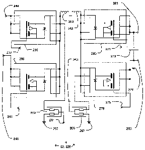
Referring to Fig. 3a, battery control first portion 225 includes input 249;
outputs 233,
234, 236, 250; ground (digital or analog, as appropriate) 243; resistor 251;
capacitor 231; DC
jack terminals 227, 247; and input overvoltage protection circuit 229; and
Metal Oxide
Semiconductor Field Effect Transistor ("MOSFET") 245. The circuit elements of
the battery
control first portion are electrically interconnected as shown in Fig. 3a.
Preferred electrical characteristics for some of the components of the first
battery control
portion are now set forth in parentheses after each element: input 249
(Overcharge); output 233
(Charge Supply); output 234 (input 244); output 236 (input 246); output 250
(Jack Sense); and
resistor 251 (1M0).
Capacitor 231 is preferably formed as a set of four parallel-connected
capacitors,
including two variable capacitors and two fixed 10 F capacitors. Jack
terminals 227, 247 allow
the positive side of the input / output to be connected to external components
(such as charging,
sources and discharging loads). Input overvoltage protection circuit 229
includes two transorbs
and a polyswitch as shown in Fig. 3a. The transorbs behave like Zener diodes
and will give off
heat as voltage increases into an overvoltage. The polyswitch acts as a
resettable thermal fuse. In
CA 02575837 2007-02-01
WO 2006/012736 PCT/CA2005/001183
13
the event of overvoltage, heat from the transorbs trips the polyswitch to
thereby eliminate the
overvoltage condition. Alternatively, other types of overvoltage protection,
now known or to be
developed in the future, could be used. MOSFET 245 prevents overcharge and is
basically a
switch that turns off in the event of potential overcharging. MOSFET 245 is
preferably
constructed as Model Si4886DY from Vishay Siliconix of Shelton, Connecticut.
Referring to Fig. 3b, battery control second portion 226 includes inputs 237,
241, 244,
246, 271, 275, 281, 283; outputs 261, 263; capacitor 273 (preferably
constructed similar to
capacitor 231); inductors 253, 255; grounds (digital or analog, as
appropriate) 257, 267, 277;
precision voltage dividers 259, 265; and MOSFETs 235, 239, 269, 279. The
circuit elements of
the battery control second portion are electrically interconnected as shown in
Fig. 3b. Preferred
electrical characteristics for some of the elements of the battery control
second portion are now
set forth in parentheses after each element: input 237 (Series a Gate); input
241 (Shunt a Gate);
input 244 (output 234); input 246 (output 236); input 271 (Series B Gate);
input 275 (Shunt B
Gate); output 261 (Node A Signal); output 263 (Node B Signal); input 281
(Battery +); and input
283 (Battery -).
MOSFETS 235, 269 are preferably constructed as Model Si4835DY from Vishay
Siliconix. MOSFETS 239, 279 are preferably constructed as Model Si4886DY from
Vishay
Siliconix. Inductors 253, 255 are preferably each 3.2 microhenry inductors
with a saturation
current of at least 8.6 amperes (A) at 25 degrees Celsius (C). Of course, the
combined
) inductance of these inductors connected in series is 6.4 microhenry.
Alternatively, one larger
inductor could be used here, but it is generally easier to obtain two small
inductors rated at this
high level of saturation current. Precision voltage dividers 259, 265 (or
resistor networks) are
preferably constructed as Model MPM2001/1002A from Vishay Thin Film of
Shelton,
Connecticut. In power supply 50, these MOSFETS 235, 239, 269, 279 are the
power supply
switches. In other power supply embodiments, other types of FETs, or other
types of transistors,
or even entirely different types of semiconductor devices, may be used for the
power supply
switches. Power supply switches are sometimes herein referred to as "power
supply switch
FETs."
Now that the circuitry of battery contro1225, 226 has been identified, its
primary
J functionality will be briefly discussed. Switching power supplies use
passive (e.g., inductors,
capacitors) and active (e.g., switches) components, working in conjunction, to
accomplish the
CA 02575837 2007-02-01
WO 2006/012736 PCT/CA2005/001183
14
desired regulation (generally voltage regulation). In power supply 50, the
passive components
are capacitors 231, 271 and inductors 253, 255. The MOSFETs 235, 239, 269, 279
are the active
components, or switches, of switching power supply 50. These four MOSFETs are
structured to
accomplish the five modes operation of power supply operation as identified
above.
The precision voltage dividers 259, 265 are used to divide the Voltages on
either side of
the inductor. The inductor voltage is used to predict a zero current condition
and thereby help
control in the efficient operation of the switching power supply. However, the
voltage is divided
because it is a high voltage that could damage the components used in making
the zero current
predictions. Alternatively, other hardware, now known or to be developed in
the future, could be
used to effect any necessary voltage decreases required by the zero current
prediction circuitry.
Preferred switching power supplies according to the present invention have
electrical
power efficiencies (e.g., at 25 watt, full power) of upwards of 95%, 98% or
even 99%. Some of
the features that result in the very high efficiencies of the present
invention are related to the
driving of the power supply switches, in this embodiment MOSFETs 235, 239,
269, 279. Some
inefficiencies in switching power supplies include: (1) gate charge of MOSFETS
(active
component set, frequency sensitive); (2) resistance drain to source ("RDS",
active component
set); (3) resistance loss of inductor (dc loss, frequency sensitive, less loss
at high frequency); (4)
capacitive losses (frequency sensitive, ESR: effective series resistance); (5)
shunt loss (smaller
shunt is preferred, not frequency sensitive); and (6) frequency inductance.
0 The transient resistance of the MOSFETs cause switching losses. The present
invention
reduces these switching losses through the use of high speed switching (>15
nanosecond rising
edge, >10 nanosecond rising edge) and driver circuitry capable of fast, clean
operation.
Phantom switching in the MOSFETs is another source of switching losses. The
present
operation compensates for phantom switching by overbiasing the gate voltages
of the MOSFET
power supply switches. Specifically, the gate voltage is adjusted, or biased,
by some amount
(typically 2 V) from the nominally expected values in whatever direction (+V, -
V) will tend to
compensate for phantom switching.
A schematic 1900 of power supply switch MOSFETs 235, 239, 269, 279 is shown in
Fig.
41. There is in each MOSFET an inherent source-to-drain capacitance 1902, an
inherent gate-to-
~ source capacitance 1904 and an inherent gate-to-drain capacitance 1906.
Please note that 1902,
1904 and 1906 are not separate components, but rather hypothetical components
that model the
CA 02575837 2007-02-01
WO 2006/012736 PCT/CA2005/001183
way charge behaves inside a FET. The ratio of gate-to-source capacitance to
gate-to-drain
capacitance is herein called the gate capacitance ratio. In a power supply
switch that is high side
referenced so that the gate voltage is nominally referenced to the drain
voltage, the gate voltage
will tend to be pulled toward the source voltage by the gate capacitance
effect. The gate
capacitance effect is the absolute value of the difference between the source
and drain voltages
multiplied by the gate capacitance ratio. The smaller the gate capacitance
ratio (e.g. >0.1,
>0.05), the less the gate voltage will be pulled toward the source voltage.
While making a smaller gate capacitance ratio is one way to reduce the gate
capacitance
effect, overbiasing the gate reference voltage is a way to systematically
compensate for the gate
capacitance effect. More particularly, the driving circuitry that generates
the gate reference
voltage preferably offsets (i.e., offsets away from the source voltage level)
the gate reference
voltage in an amount approximately equal to the gate capacitance effect. For
example, if source
is at ground level and drain is at 20 V, and the gate capacitance ratio is
0.05, then gate
capacitance effect equals 120V-0VI * 0.05 = 1 volt. Therefore, the gate
reference voltage would
be about 20V + 1 V= 21 V at this point to make up for the gate capacitance
effect. Overbiasing
of the gate is especially helpful when multiple power supply switches and
synchronous operation
give rise to the possibility of phantom switching because the overbiasing
helps eliminate or
reduce phantom switching.
Referring to Fig. 4, display and equalization first portion 300 includes
inputs 322, 324,
0 330; outputs 306, 308, 310, 312; terminals 320, 350; ground (preferably
digital) 304; resistors
314, 316, 318, 326, 332, 336, 340, 344, 348, 352, 354, 356, 358; light
emitting diodes (LEDs)
328, 334, 338, 342, 346; and sixteen port processing circuit 302. The circuit
elements of the
display and equalization first portion are electrically interconnected as
shown in Fig. 4.
Preferred electrical characteristics for some of the elements of the display
and equalization first
S portion are now set forth in parentheses after each element: input 322
(Serial Data Port B); input
324 (Serial Clock Port B); input 330 (LED 1); output 306 (Equalization
4);.output 308
(Equalization 3); output 310 (Equalization 2); output 312 (Equalization 1);
terminal 320 (+5.4
V); terminal 350 (+5.4 V); resistor 314 (IOOK); resistor 316 (100K); resistor
318 (100K);
resistor 326 (100K); resistor 332 (1K0); resistor 336 (1K0); resistor 340
(1K0); resistor 344
~ (1K0); resistor 348 (1K0); resistor 352 (100K); resistor 354 (100K);
resistor 356 (100K); resistor
358 (100K); LED 328 (Red); LED 334 (Yellow); LED 338 (Green); LED 342 (Green);
LED 346
CA 02575837 2007-02-01
WO 2006/012736 PCT/CA2005/001183
16
(Green); port 1 of circuit (or "ckt") 302 (AO); port 2 of ckt 302 (Al); port 3
of ckt 302 (A2); port
4 of ckt 302 (LEDO); port 5 of ckt 302 (LED1); port 6 of ckt 302 (LED2); port
7 of ckt 302
(LED3); port 8of ckt 302 (GND); port 9 of ckt 302 (LED4); port 10 of ckt 302
(LED5); port 11
of ckt 302 (LED6); port 12 of ckt 302 (LED7); port 13 of ckt 302 (RESET); port
14 of ckt 302
(SCL); port 15 of ckt 302 (SDA); and port 16 of ckt 302 (VDD).
Processing circuit 302 is preferably structured as an 8-bit 12C LED Driver
(with
programmable blink rates), model PCA9551 made by Philips Semiconductors of the
Netherlands. Processing circuit 302 receives signals in 12C, serial format
from the main
microprocessor and converts these into parallel signals, such as: (1) parallel
signals used to
control LEDs 328, 334, 338, 342, 346; and (2) parallel signals used to control
charging
equalization (further discussed below). The 12C format signal are input to
processing circuit 302
through ports 14 and 15. The parallel signals for controlling the LEDs are
output through
processing circuit 302 ports 9 to 18. The parallel signals for controlling
charging equalization
are output through processing circuit 302 ports 4 to 7. One feature of the 12C
to parallel
communications interface of processing circuit 302 is that it separates the
LED drive circuitry
from direct microprocessor current. This is beneficial because the
microprocessor typically
makes very sensitive voltage measurements. Another feature of the 12C to
parallel
communications interface of processing circuit 302 is that this scheme frees
up m.icroprocessor
pins because the serial I2C version of the communications, output by the
microprocessor)
requires fewer pins than the parallel LED-related and equalization-related
versions of the same
communications as output by processing circuit 302.
Fig. 5 shows decoupling capacitor set 375 including +5.4 V terminal 381,
ground 383;
0.1 microfarad (gF) capacitor 377; and 1 gF capacitor 379. Capacitors 377 and
379 are
connected in parallel. Capacitor set 375 is connected between the +5.4 supply
rail and digital
ground, electrically proximate to processing circuit 302. The use of both 0.1
F and 1 F
capacitors causes decoupling at both high and low frequencies.
Referring to Fig. 6, display and equalization second portion 400 includes
inputs 416, 426,
436, 446; outputs 408, 410, 452, 454, 456, 458, 460; terminals 419, 429, 439,
449; grounds
(preferably digital) 406, 412, 422, 432, 442; resistors 404, 418, 420, 428,
430, 438, 440, 448,
450; NPN bipolar transistors 414, 424, 434, 444; and ten port connector 402.
The circuit
elements of the display and equalization second portion are electrically
interconnected as shown
CA 02575837 2007-02-01
WO 2006/012736 PCT/CA2005/001183
17
in Fig. lb. Preferred electrical characteristics for some of the elements of
the display and
equalization second portion are now set forth in parentheses after each
element: input 416
(Equalization 1); input 426 (Equalization 2); input 436 (Equalization 3);
input 446 (Equalization
4); output 408 (Battery-); output 410 (IS+); output 452 (Cell 1); output 454
(not connected);
output 456 (Battery+); output 458 (Cell 3); output 460 (Cell 2); terminal 419
(+5.4 V); terminal
429 (+5.4 V); terminal 439 (+5.4 V); terminal 449 (+5.4 V); resistor 404 (5
mOhm Cu Track);
resistor 418 (301K); resistor 420 (OR); resistor 428 (301K); resistor 430
(OR); resistor 438
(301K); resistor 440 (301K); resistor 448 (301K); and resistor 450 (301K).
Connector 402 is preferably structured as a 2 by 5, 25 square header
connector. The
circuitry and electronics of power supply 50 are preferably mounted on a
control board (not
shown). The electrochemical cells charged and discharged by power supply 50
are preferably
mounted on an interconnect board (or frame). Connector 402 (mounted on the
control board)
electrically connects the control board to the interconnect board, and to the
electrochemical cells
(preferably four connected in series) themselves. Transistors 414, 424, 434,
444 act as switches
for equalization resistors (not shown in Fig. 6, but preferably located on the
control board).
More particularly, it is preferred that the electrochemical cells charge at
(at least) roughly
even rates and/or at a roughly equal charged capacity over the recharging
process. Therefore, an
equalization resistor is selectively connected in parallel with each
electrochemical cell. When an
electrochemical cell is charging too quickly, the parallel bypass resistor can
be turned on by the
corresponding transistor 414, 424, 434, 444. If an electrochemical cell is
charging too slowly
then its bypass resistor can be disconnected by turning off the corresponding
transistor switch.
As mentioned previously, the paraIlel format equalization signals EQ1, EQ2,
EQ3, EQ4 to
control the on-off state of the transistors is received from processing
circuit 302 based on 12C
signals from the microprocessor. In this way, the microprocessor controls cell
charging rates
and/or relative charged capacities. It is noted that in other embodiments,
other types of charging
control may be desired (e.g., preferentially charge / discharge one of the
cells relative to the
others). The above-discussed control signals and transistors 414, 424, 434,
444 also provide a
mechanism to effect these other, non-preferred types of control.
Four FET driver circuits 475, 525, 575, 625 will now be explained with
reference to Figs.
7, 8, 9 and 10, respectively. Referring to Fig. 7, first FET driver 475
includes input 496; output
519; ground (preferably analog) 515; resistors 481, 487, 489, 493, 495, 503,
507, 511, 523;
CA 02575837 2007-02-01
WO 2006/012736 PCT/CA2005/001183
18
capacitors 479, 513; terminals 477, 491, 501, 505; diode 483; bipolar
transistors 517, 521; and
FETs 485, 497, 499, 509, 510. Preferred electrical characteristics for some of
the elements of
first FET driver 475 are set forth in parentheses in the following list: input
496 (Seriesa_In);
output 519 (Seriesa Gate); resistor 481 (4K99); resistor 487 (301K); resistor
489 (100K);
resistor 493 (24R9); resistor 495 (301K); resistor 503 (24R9); resistor 507
(4K99); resistor 511
(100K); resistor 523 (100K); capacitor 479 (1000 pF); capacitor 513 (0.01 F);
termina1477
(V 1+); terminal 491 (V 1+); terminal 501 (V 1-); and terminal 505 (V 1-).
Diode 483 is preferably
model number BAV70 (see webpage
http://www.fairchildsemmi..com/cqpfBA/BAV70.html for
further information on component BAV70). Bipolar transistor 517 is preferably
model number
FMMT619CT. Bipolar transistor 521 is preferably model number FMMT720CT.
Referring to Fig. 8, second FET driver 525 includes input 546; output 569;
ground
(preferably analog) 565; resistors 531, 537, 539, 543, 545, 553, 557, 561,
573; capacitors 554,
529, 563; terminals 527, 541, 551, 555; diode 533; bipolar transistors 567,
571; and FETs 535,
547, 549, 559, 560. Preferred electrical characteristics for some of the
elements of second FET
driver 525 are set forth in parentheses in the following list: input 546
(Seriesb_ln); output 569
(Seriesb_Gate); resistor 531 (4K99); resistor 537 (301K); resistor 539 (100K);
resistor 543
(24R9); resistor 545 (301K); resistor 553 (24R9); resistor 557 (4K99);
resistor 561 (100K);
resistor 573 (100K); capacitor 554 (1000 pF); capacitor 529 (1000 pF);
capacitor 563 (0.01 F);
terminal 527 (V3+); terminal 541 (V3+); terminal 551 (V3-); and terminal 555
(V3-). Diode 533
is preferably model number BAV70. Bipolar transistor 567 is preferably model
number
FMMT619CT. Bipolar transistor 571 is preferably model number FMMT720CT.
Referring to Fig. 9, third FET driver 575 includes input 596; output 619;
resistors 581,
587, 589, 593, 595, 603, 607, 623; capacitors 604, 579; terminals 577, 591,
601, 605; diodes 583,
610; bipolar transistors 617, 621; and FETs 585, 597, 599, 609. Preferred
electrical
characteristics for some of the elements of third FET driver 575 are set forth
in parentheses in the
following list: input 596 (Shunta_In); output 619 (Shunta Gate); resistor 581
(4K99); resistor
587 (301K); resistor 589 (301K); resistor 593 (24R9); resistor 595 (DNP);
resistor 603 (24R9);
resistor 607 (4K99); resistor 623 (100K); capacitor 604 (1000 pF); capacitor
579 (1000 pF);
tem-iina1577 (V2+); terminal 591 (V2+); terminal 601 (V2-); and terminal 605
(V2-). Diodes
583, 610 are preferably model number BAV70. Bipolar transistor 617 is
preferably model
number FMMT619CT. Bipolar transistor 621 is preferably model number FMMT720CT.
CA 02575837 2007-02-01
WO 2006/012736 PCT/CA2005/001183
19
Referring to Fig. 10, fourth FET driver 625 includes input 646; output 669;
resistors 631,
637, 639, 643, 645, 653, 657, 673; capacitors 654, 629; terminals 627, 641,
651, 655; diodes 633,
660; bipolar transistors 667, 671; and FETs 635, 647, 649, 659. Preferred
electrical
characteristics for some of the elements of fourth FET driver 625 are set
forth in parentheses in
the following list: input 646 (Shuntb_ln); output 669 (Shuntb_Gate); resistor
631 (4K99);
resistor 637 (301K); resistor 639 (301K); resistor 643 (24R9); resistor 645
(DNP); resistor 653
(24R9); resistor 657 (4K99); resistor 673 (100K); capacitor 654 (1000 pF);
capacitor 629 (1000
pF); terminal 627 (V2+); terminal 641 (V2+); terminal 651 (V2-); and
teriizinal 655 (V2-).
Diodes 633, 660 are preferably model number BAV70. Bipolar transistor 667 is
preferably
model number FMMT619CT. Bipolar transistor 671 is preferably model number
FMMT720CT.
The four FET drivers 475, 525, 575, 625 respectively handle control signals
for the four
power supply switches, specifically MOSFETS 235, 269, 239, 279 (see Fig. 3b
and related
discussion). The operation of each of the four FET drivers is quite similar,
so only the operation
of FET driver 475 will be discussed now in detail. FET driver 475 handles
control output
signals, that is, the signals sent from the controller to a power supply
switch (in this example,
MOSFET 235) to control the on-off operation of that power supply switch. More
particularly,
the some features of FET driver 475 relate to: (1) a capacitive coupling in
the path transmitting
the control output signal; (2) use of a pinkeeper circuitry in the path
transmitting the control
output signal; and/or (3) use of a path suitable for draining gate capacitance
charge from a power
supply switch. It should be kept in mind that at least some of the features
explained in this
context will have applicability to other switching power supplies (now extant
and to be
developed in the future) having various hardware layouts, topologies, etc.
This conversion of the control output signals from one form to another by FET
driver 475
will now be explained. Specifically, the conversion of the Seriesa Tn control
output signal 496
into the form of the corresponding Seriesa Gate control output signal 519 will
be explained with
reference to Fig. 7. FET driver 475 may be more generically referred to as a
power supply
switch driver. As shown in Fig. 7, the Seriesa In signal 496 (from the
controller) is provided as
an input at the left side of FET driver 475. FET driver 475 converts the
Seriesa In signal into
the corresponding Seriesa_Gate signa1519, which is provided as an output on
the right side of
FET driver 475. Three aspects of FET driver 475 will now be discussed: (1)
capacitive
CA 02575837 2007-02-01
WO 2006/012736 PCT/CA2005/001183
coupling; (2) pinkeeper; and (3) path suitable for draining gate capacitance
charge from a power
supply switch.
FET driver 475 includes capacitors 479, 504. These two capacitors form a
capacitive
coupling (alternatively, there could be more or fewer individual capacitors in
the capacitive
coupling). More particularly, there is no direct (or dc) path between the
Seriesa-In input 496 and
the Seriesa Gate output 519. Communication of the control output signal
therefore goes through
this capacitive coupling.
In the preferred embodiment, the Seriesa-In signal is in the form of a 5 volt,
digital
ground referenced square wave (e.g., 0 volts for off, 5 V for on). Most of the
time, during the
flat stay-off or stay-on portions, this Seriesa-In square wave signal has only
a dc component.
This dc component does not get communicated through the capacitive coupling.
However, the
rising and falling of the square wave involve high frequency components, as
would be revealed
by a Fast Fourier Transform. These high frequency components, these rising or
falling edges,
are communicated through the capacitive coupling. Specifically, the rising and
falling edges
cause short duration positive and negative voltage spikes on the right side of
FET driver 475.
Therefore, in this preferred embodiment, wherein a square wave format control
output
signal is communicated through a capacitive coupling to become a signal
characterized by
voltage spikes (herein called an intermediate control output signal because it
is an intermediate
form of the control output signal between the Seriesa In. form and the
Seriesa_Gate form).
However, it is noted that alternative embodiments may use other electrical
signal patterns, while
still effecting communication through a capacitive coupling. For example, the
control output
signal could be in the form of voltage spikes prior to being communicated by
the capacitive
coupling. At least in theory, any control output signal with a substantial
high frequency
component can be comn-iunicated through a capacitive coupling in some fashion.
At least theoretically, the intermediate control output signal could directly
be used to
control a power supply switch. Of course, the power supply switch would need
to be designed to
be turned on or off (and quickly so) by positive and negative voltage spikes.
Such an
embodiment of the present invention would potentially have many of the
advantages of
capacitive coupling, as will be explained below. However, in power supply 50,
the power supply
switches are constructed as FETs 235, 269, 239, 279, which are referenced at
around the
relatively high voltages of electrochemical cells (e.g., lOV to 20V). The
voltage spikes of the
CA 02575837 2007-02-01
WO 2006/012736 PCT/CA2005/001183
21
intermediate signal are insufficient to directly control the FET power supply
switches of
preferred embodiment 50 for reasons including the following: (1) the amplitude
(that is, absolute
voltage level) of the spikes are too low to operate the power supply switch
FET (which is
operating at battery voltage type levels); and (2) the spikes have a short
time duration, while the
gate terminal of the power supply switch FET must be driven by a continuous
voltage.
In order to make the spike-form intermediate control output signal control the
power
supply switch 235, the intermediate control output signal is converted into
the Seriesa Gate
signal 519 by the pinkeeper circuitry included in FET driver 475. The
pinkeeper circuitry
includes FETs, bipolar transistors and resistors as shown in Fig. 7. The
principles of operation of
the pinkeeper circuitry are conventional and will therefore not now be
discussed in component
by component detail here. For present purposes, the hardware details of the
pinkeeper circuitry
isn't as important as the idea of using pinkeeper circuitry in conjunction
with a control output
signal for a power supply switch set in a switching power supply.
Generally speaking, the pinkeeper circuitry of FET driver 475 uses the
positive and
negative voltage spikes of the intermediate control output signal to latch the
Seriesa_Gate control
output signal at a high or a low level. The voltage values for the high and
low levels will depend
upon battery voltage, power supply FET switch polarity, overbiasing and so on.
The FET driver
circuitry is typically where the overbiasing of the gate reference voltage to
compensate for gate
capacitance effect is applied to the driver signal. The latched Seriesa Gate
signal is applied to
) the gate terminal of the series a power supply FET switch 235. When Seriesa
Gate is latched in
one voltage state (say, low voltage level), this turns and maintains the power
supply FET switch
off. When Seriesa_Gate is latched in the other voltage state (say, high
voltage level), this turns
and maintains the power supply FET switch on. The pinkeeper circuitry is bi-
stable. That is, the
pinkeeper circuitry reliably maintains Seriesa Gate in a high or low (that is,
on or off) state,
changing only in response to spikes in the intermediate control output signal.
Now that the operation of the capacitive coupling and the pinkeeper circuitry
have been
discussed, discussion will move to the path suitable for draining gate
capacitance charge from a
power supply switch, built into FET driver 475. Assume that a step change in
the voltage of the
Seriesa In. control output signal causes a voltage spike in the intermediate
control output signal.
) This spike turns on FET 509 (see Fig. 7). Turning on FET 509 causes current
to be pulled
through bipolar transistor 521. Pulling current through bipolar resistor 521
pulls the
CA 02575837 2007-02-01
WO 2006/012736 PCT/CA2005/001183
22
Seriesa_Gate control output signal down toward voltage level V1-. When the
Seriesa_Gate
signal reaches voltage V 1- it will turn the Seriesa power supply FET switch
235 on or off
(depending on polarity of the series a power supply FET switch). In this
electrical scheme, FET
509 is a low impedance path. This current drain quickly drains the gate
capacitance of the series
a power supply FET switch.
Because the gate capacitance is quickly drained, the Series_a power supply FET
switch
509 turns on and off quickly. Also, any overbiasing of the gate capacitance
will be accomplished
more quickly because of the low impedance current path. This quick on-off
operation of the
power supply FET switch 509 reduces switching losses and/or transition losses
and thereby
improves efficiency. For example, a rise time as low as 10 nanoseconds has
been observed.
That is very quick.
The capacitive coupling, pinkeeper and current path features embodied in
conversion
circuitry 202 (whether considered individually or in combination) has several
potential
objectives, features and/or advantages:
(1) Control output signal can be generated at one reference level by the
controller
circuitry (e.g., digital ground referenced), but can still control a power
supply switch referenced
at a different level (e.g., power supply FET switch referenced at the analog
voltage of an
electrochemical cell); the feature of having two (or more) different reference
levels for a control
output signal is facilitated by the capacitive coupling;
(2) Control output signal can be generated at one voltage amplitude level by
the
controller circuitry (e.g., 5 V over digital ground for on), but can still
control a power supply
switch responsive to a different level control signal (e.g., power supply FET
switch operated
with overbiasing); the feature of having two (or more) different amplitude
levels for a control
output signal is facilitated by the capacitive coupling;
(3) The control output signal generated by the controller does not need to
actively and/or
continuously drive the power supply switch; this feature is facilitated by the
pinkeeper and its
latching;
(4) Switching losses and associated rise and fall times associated with the
switching of a
power supply switch are reduced; this is facilitated by the capacitive
coupling; for example, the
) capacitive coupling facilitates a reduction in switching losses in the sense
that the control output
signal reference level and amplitude level can be manipulated by virtue of the
capacitive
CA 02575837 2007-02-01
WO 2006/012736 PCT/CA2005/001183
23
coupling so that faster power supply switch driver components can be chosen
and/or so that
power supply switch driver components can be operated well below their voltage
and/or speed
limitations;
(5) Switching losses and associated rise and fall times associated with the
switching of a
power supply switch are reduced; this is facilitated by the low impedance path
and/or appropriate
capacitors for alternately draining and supplying charge of the gate
capacitance of the power
supply switch (e.g., FET switch);
(6) Allows quicker and/or amore accurate overbiasing of power supply switch
(e.g.,
power supply FET switch);
(7) Prevents phantom switching;
(8) Improves power supply efficiency and reduces heat generated in power
supply switch
(e.g., FET switch) during rides and falls of the operative control output
signal;
(9) Bipolar transistor used to help form a low impedance path for gate
capacitance of a
power supply switch; and
(10) use of what is effectively a high gain current amplifier.
Figs. 11 to 14 show capacitor sets 800, 825, 850, 875 respectively used in
conjunction
with FET drivers 235, 239, 269, 279. The capacitor sets 800, 825, 850, 875
absorb the gate
capacitance of a corresponding power supply FET switch 235, 239, 269, 279 when
it is turned
off. The capacitor sets also supply charge to help restore the gate
capacitance when the
- corresponding power supply FET switch is turned on again. For example,
capacitor set 800 is
connected across the V 1+ / V 1- terminals of FET driver 475 and exchanges
charge with the
Seriesa power supply FET switch 235. Fig. 11 shows capacitor set 800 including
Vl+ terminal
802, V 1- termina1808, Charge Supply input 814, 0.1 F capacitors 804, 808 and
0.01 gF
capacitors 810, 812. Fig. 12 shows capacitor set 825 including V2+ terminal
827, V2- terminal
833, ground 837, 0.1 F capacitors 829, 831 and 0.01 pF capacitors 835, 839.
Fig. 13 shows
capacitor set 850 including V2+ terminal 852, V2- termina1858, ground 862, 0.1
F capacitors
854, 856 and 0.01 F capacitors 860, 864. Fig. 14 shows capacitor set 875
including V3+
terminal 877, V3- terminal 883, Battery+ input 887, 0.1 gF capacitors 879, 881
and 0.01 gF
capacitors 885, 889.
Fig. 15 shows Batt- input 895 and ground 897. The circuitry of Fig. 15
connects the Batt-
signal to a (preferably analog) ground.
CA 02575837 2007-02-01
WO 2006/012736 PCT/CA2005/001183
24
The circuitry of Figs. 16 to 19 will now be explained by first identifying the
constituent
components in each of the Figs., followed by discussion of the operation of
the circuitry and its
role in switching power supply 50.
Referring to Fig. 16, isolated power supply transformer circuitry 900 includes
inputs 906,
934, 936; output 928; terminals 904, 918, 945; ground (preferably digital)
912; resistors 908,
914, 920, 948; capacitors 910, 916, 938, 949; core / winding assemblies 922,
940; diodes 930,
932; Schottky diode 946; and switch mode regulator 902. The circuit elements
of the isolated
power supply transformer circuitry are electrically interconnected as shown in
Fig. 16. Preferred
electrical characteristics for some of the elements of isolated power supply
transformer circuitry
900 are set forth in parentheses in the following list: input 906
(Power_Enable); input 934
(Batt+); input 936 (Charge_Supply); output 928 (Control Power); terminal 904
(+4.7 V);
terminal 918 (+5.4 V_; terminal 945 (+5.4 V); resistor 908 (IOOK); resistor
914 (lOKO); resistor
920 (33K2); resistor 948 (10R0); capacitor 910 (10 F); capacitor 916 (4.7
pF); capacitor 938 (1
F); capacitor 949 (10 F); port 1 of regulator 902 (SW); port 2 of regulator
902 (GND); port 3
of regulator 902 (FB); port 4 of regulator 902 (VIN); and port 5 of regulator
902 (SHDN). Diode
930, 932 are preferably model number BAV70. Schottky diode 946 is preferably
model number
MA112CT. Core / winding assembly 922 is preferably model number T1A F4E-
1810B+F4IE-
1810B. Core / winding assembly 940 is preferably model number T1E. Core /
winding
assemblies 922 and 940 include taps 924, 926, 942, 944, which taps will be
further discussed
below.
Referring to Fig. 17, first tap circuitry 950 includes input 962; Schottky
diodes 954, 972;
terminals 960, 966; resistors 956, 970; Zener diode 964; capacitors 958, 968
and core / winding
assembly 952. The circuit elements of the first tap circuitry are electrically
interconnected as
shown in Fig. 17. Preferred electrical characteristics for some of the
elements of first tap
circuitry 950 are set forth in parentheses in the following list: input 962
(Charge Supply);
termina1960 (Vl+); terminal 966 (V1-); resistor 956 (10R0); resistor 970
(10R0); capacitor 958
(1 F); and capacitor 968 (1 F). Schottky diodes 954, 972 are preferably
model number
MAl 12CT. Zener diode 964 is preferably model number BZX84C10-7. Further
information on
this component can be found at webpage:
http://www.allamerican.com/direct/product.asp?T_PRDKEY=DIO+BZX84C107+++++++++++
&T MFGCOD=DIO+&T PRDID=BZX84C 10-7+++++++++++.
CA 02575837 2007-02-01
WO 2006/012736 PCT/CA2005/001183
Core / winding assembly 952 will be further discussed below.
Referring to Fig. 18, second tap circuitry 975 includes circuit elements 979,
981, 983,
989, 993, 995, 997 which are similar to their counterparts in circuitry 950
identified above in
connection with Fig. 17. The second tap circuitry further includes V2+
termina1985, V2-
terminal 991 and (preferably analog) ground 995. The circuit elements of the
second tap
circuitry are electrically interconnected as shown in Fig. 18. Core I winding
assembly 977 will
be further discussed below.
Referring to Fig. 19, third tap circuitry 1000 includes circuit elements 1004,
1006, 1008,
1014, 1018, 1020, 1022 which are similar to their counterparts in circuitry
950 discussed above
in connection with Fig. 17. The third tap circuitry further includes V3+
terminal 1010, V3-
terminal 1016 and Battery+ input 1012. The circuit elements of the third tap
circuitry are
electrically interconnected as shown in Fig. 19. Core / winding assembly 1002
will be further
discussed below.
Now that the isolated power supply circuitry 900, 950, 975, 1000 has been
identified, its
functionality will be discussed. The isolated power supply circuitry receives
input electrical,
which it converts into power signals of six voltage levels: Vl+. V1-, V2+, V2-
, V3+ and V3-.
These six voltages are used to provide bias voltages and otherwise drive the
power supply
switches of power supply 50, specifically MOSFETs 235, 239, 245, 269 and 279
(see Figs. 3a
and 3b).
~ More particularly, input 906 is a digital power enable signal that controls
the on or off
status of MOSFETs 235, 239, 245, 269, 279. Input 934 is Batt+, the power from
the series
connected string of electrochemical cells downstream of power supply 50. Input
932
Charge_Supply, is the power from the i/o jack. Diodes 930 and 932 effectively
select whether
Batt+ power or Charge_Supply power is used in the isolated power supply
circuitry. Output 928
5 sends some of the electrical power to the microprocessor as Control_Power
(see Fig. 22 at input
1171).
The electrical power from Batt+ 930 and/or Charge_Supply 936 is transformed
into the
six voltage levels by core / winding assemblies 922, 940, 952, 977 and 1002.
These five core /
winding assemblies utilize coils built into the board (not shown) that
physically supports the
) various components of power supply 50. All five coils are adjacent to a
common core. As will
be understood by those of skill in the art, the electromagnetic interaction at
the five core /
CA 02575837 2007-02-01
WO 2006/012736 PCT/CA2005/001183
26
winding assemblies, working in conjunction with the other components of Figs.
16-19,
transforms the power from Batt+ and/or Charge_Supply into the six voltage
signals respectively
at terminals 960, 966, 985, 991, 1010, 1016.
The core / winding assemblies of Figs. 16 to 19 means that the six voltage
signals Vl+/-,
V2+/-, V3+/- are not necessarily referenced to the voltage level of the Batt+
and Charge_Supply
power inputs. Rather: (1) V 1+/- signals happen to be referenced to
Charge_Supply (because
Charge_Supply is provided at input 962, not because of the use of
Charge_Supply as input
power); (2) V2+/- signals are referenced to an AC high frequency ground; and
(3) V3+/- signals
happen to be referenced to Batt+ (because Batt+ is provided at input 962, not
because of the use
of Batt+ as input power). This carefully controlled reference voltage level
for the six voltage
signals is important because these six signals operate and bias MOSFETs 235,
239, 245, 269,
279. As will be understood by those of skill in the art upon a review of Figs.
3a and 3b, each of
the MOSFETs must be referenced to the appropriate level (Charge_Supply, high
frequency
ground, Batt+) regardless of whether the power supplied through isolated power
supply circuitry
900, 950, 975, 1000 comes from Charge_Supply or from Batt+ at any given point
of time.
In this exemplary embodiment of power supply 50, isolated power supply
circuitry 900,
950, 975, 1000 has a SEPIC configuration (see capacitor 938 at Fig. 16).
Alternatively, flyback
or other configurations, now known or to be developed in the future, could be
used in the
isolated power supply circuitry, but SEPIC will often be the most energy
efficient configuration.
The microcontroller circuitry 1025, 1100, 1125 of Figs. 20 to 22 will now be
explained
by first identifying the constituent components in each of the Figs., followed
by discussion of the
operation of the microcontroller circuitry and its role in switching power
supply 50.
Microcontroller circuitry first portion 1025 includes analog circuitry
connected to ports 1-3, 20-
23, 25, 27 and 28 of 28-port microcontroller 1027. Microcontroller- circuitry
second portion
1100 includes analog circuitry connected to ports 24 and 26 of 28-port
microcontroller 1027.
Microcontroller circuitry third portion 1125 includes digital circuitry
connected to ports 4-19 of
28-port microcontroller 1027.
Referring to Fig. 20, microcontroller circuitry first portion 1025 includes
inputs 1029,
1031, 1053, 1055, 1069, 1079; ground (analog or digital as appropriate) 1037,
1049, 1059, 1065,
1073; resistors 1033, 1035, 1051, 1053, 1063, 1067, 1071, 1077; capacitors
1039, 1041, 1043,
1045, 1047, 1057, 1061, 1075; and 28-port microcontroller 1027. The circuit
elements of the
CA 02575837 2007-02-01
WO 2006/012736 PCT/CA2005/001183
27
microcontroller circuitry first portion are electrically interconnected as
shown in Fig. 20.
Preferred electrical characteristics for some of the elements of
microcontroller circuitry first
portion 1025 are set forth in parentheses in the following list: input 1029
(IS+); input 1031
(Cell_1); input 1053 (lreg_monitor); input 1055 (IS+); input 1069 (Cell_3);
input 1079 (Cell_2);
resistor 1033 (301K); resistor 1035 (301K); resistor 1051 (143K); resistor
1053 (121R); resistor
1063 (143K); resistor 1067 (1M0); resistor 1071 (150K); resistor 1077 (453K);
capacitor 1039 (1
F); capacitor 1041 (1 F); capacitor 1043 (1 F); capacitor 1045(0.47 F);
capacitor 1047 (1
F); capacitor 1057 (0.47 F); capacitor 1061 (1 F); capacitor 1075 (1 F);
rnicrocontroller port
1(RAlANl); microcontroller port 2 (RAO/ANO); microcontroller port 3(RD3/REFB);
microcontroller port 20 (Vss); microcontroller port 21 (SUM); microcontroller
port 22 (CDAC);
microcontroller port 23 (RD7/AN7); microcontroller port 25 (RD5/AN5);
microcontroller port
27 (RA3AN3); and microcontroller port 28 (RA2AN2).
Referring to Fig. 21, microcontroller circuitry second portion 1100 includes
inputs 1112,
1116; ground (preferably analog) 1115; resistors 1106, 1108, 1110, 1114;
capacitors 1102, 1104;
and 28-port microcontroller 1027. The circuit elements of the microcontroller
circuitry second
portion are electrically interconnected as shown in Fig. 21. Preferred
electrical characteristics
for some of the elements of microcontroller circuitry second portion 1100 are
set forth in
parentheses in the following list: input 1112 (Charge_Supply); input 1116
(Batt+); resistor 1106
(143K); resistor 1108 (143K); resistor 1110 (1M0); resistor 1114 (1M0);
capacitor 1102 (1 F);
) capacitor 1104 (1 F); microcontroller port 24 (RD6/AN6); and
microcontroller port 26
(RD4/AN4).
Referring to Fig. 22, microcontroller circuitry third portion 1125 includes
inputs 1131,
1147, 1149, 1157, 1159, 1171, 1181; outputs 1127, 1129, 1133, 1135, 1137,
1139, 1141, 1198,
1199; terminals 1155, 1165, 1185; ground (analog or digital as appropriate)
1177, 1185, 1193;
> resistors 1143, 1145, 1151, 1153, 1161, 1163, 1169, 1173, 1179, 1189, 1195,
1197; capacitors
1175, 1178, 1183; 28-port microcontroller 1027; component 1191; diode 1187;
and component
1167. The circuit elements of the microcontroller circuitry third portion are
electrically
interconnected as shown in Fig. 22. Preferred electrical characteristics for
some of the elements
of microcontroller circuitry third portion 1125 are set forth in parentheses
in the following list:
) input 1131 (Overcharge_monitor); input 1147 (SDAB); input 1149 (SCLB); input
1157 (SDAA);
input 1159 (SCLA); input 1171 (Control_Power); input 1181 (Jack Sense); output
1127
CA 02575837 2007-02-01
WO 2006/012736 PCT/CA2005/001183
28
(Over_Current); output 1129 (Enable); output 1133 (LEDl); output 1135
(Power_Enable);
output 1137 (Pass_Mode); output 1139 (Charge_Discharge); output 1141 (Buck
Boost); output
1198 (SCLA); output 1199 (SDAA); terminal 1155 (+5.4V); terminal 1165 (+4.7V);
terminal
1185 (+4.7V); resistor 1143 (121R); resistor 1145 (121R); resistor 1151
(100K); resistor 1153
(100K); resistor 1161 (100K); resistor 1163 (100K); resistor 1169 (121R);
resistor 1173 (2M2);
resistor 1179 (1M0); resistor 1189 (2K21); resistor 1195 (121R); resistor 1197
(121R); capacitor
1175 (0.1 F); capacitor 1178 (0.1 F); capacitor 1183 (0.01 gF);
microcontroller 1027 port 4
(RD2/CMPB); microcontroller 1027 port 5(RDl/SDAB); microcontroller 1027 port 6
(RDO/SCLB); microcontroller 1027 port 7 (OSC2/CLKOUT); microcontroller 1027
port 8
(OSCl/PBTN); microcontroller 1027 port 9 (VDD); microcontroller 1027 port 10
(VREG);
microcontroller 1027 port 11 (RC7/SDAA); microcontroller 1027 port 12
(RC6/SCLA);
microcontroller 1027 port 13 (RC5); microcontroller 1027 port 14 (MCLR/Vpp);
microcontroller
1027 port 15 (RC4); microcontroller 1027 port 16 (Power Enable);
microcontroller 1027 port 17
(Pass_Mode); microcontroller 1027 port 18 (RC1/CMPA); microcontroller 1027
port 19
(RCO/REFA); diode 1187 (preferably model number BAV70); component 1167 (model
IRLML2502).
Now that the microcontroller circuitry 1025, 1100, 1125 has been identified,
its
functionality will be briefly discussed. Microcontroller chip 1127 is
preferably model
PIC14000SS. Microcontroller 1027 controls the mode that the switching power
supply operates
- in (e.g., buck charge, buck discharge, boost charge, boost discharge) and
performs other
important control functions.
Oscillator circuitry 1200 of Fig. 23 will now be explained by first
identifying the
constituent components, followed by discussion of the operation of the
oscillator circuitry and its
role in switching power supply 50. Referring to Fig. 23, oscillator circuitry
1200 includes inputs
1206, 1208, 1232; output 1270; terminals 1204, 1214, 1226, 1242, 1252, 1262;
grounds (analog
or digital as appropriate) 1210, 1216, 1228, 1248, 1254, 1264; resistors 1218,
1222, 1230, 1234,
1238, 1240, 1244, 1246, 1256, 1266, 1268; capacitors 1220, 1236, 1258; d-a
converter 1202;
operational amplifiers 1212, 1224, 1250; and comparator 1260. The circuit
elements of the
oscillator circuitry are electrically interconnected as shown in Fig. 23.
Preferred electrical
characteristics for some of the elements of oscillator circuitry 1200 are set
fortli in parentheses in
the following list: input 1206 (SDAB); input 1208 (SCLB); input 1232
(Duty_Cycle_Control);
CA 02575837 2007-02-01
WO 2006/012736 PCT/CA2005/001183
29
output 1270 (osc_out); terminal 1204 (+5.4V); terminal 1214 (+5.4V); terminal
1226 (+5.4V);
terminal 1242 (+5.4V); terminal 1252 (+5.4V); terminal 1262 (+5.4V); resistor
1218 (1K0);
resistor 1222 (1K0); resistor 1230 (18K2); resistor 1234 (39K2); resistor 1238
(121R); resistor
1240 (IK.O); resistor 1244 (100K); resistor 1246 (100K); resistor 1256 (1K0);
resistor 1266
(100K); resistor 1268 (698K); capacitor 1220 (100 pF); capacitor 1236 (100
pF); capacitor 1258
(22pF); operational amplifier 1212 (model TC1034); operational amplifier 1224
(model
LMV710 made by National Semiconductor of Santa Clara, California); operational
amplifier
1250 (model LMV710); and comparator 1260 (model LMV7219 made by National
Semiconductor).
Now that oscillator circuitry 1200 has been identified, its functionality will
be briefly
discussed. Inputs SDAB, SCLB and Duty_Cycle_Control are input to the
oscillator circuitry to
produce output osc_out. Inputs SDAB, SCLB are I2C format inputs that represent
a voltage from
0-5 volts that forms a control signal to the oscillator. Duty_Cycle_Control is
an analog signal.
The output osc_out controls the oscillator.
Oscillator circuitry 1200 produces an oscillation signal that has a variable
duty cycle, a
variable frequency and no fixed on-time or off-time for a duty cycle. This is
different than
conventional oscillators because conventional oscillators generally have at
least one of the
following restrictions: fixed frequency, fixed on time and/or fixed off time.
By utilizing
oscillator circuitry that can produce an oscillation signal having both a
fixed frequency and no
7 fixed on or off time, the multiple modes of operation (e.g., charge buck,
charge boost, discharge
buck, discharge boost) are greatly facilitated. For example, because there are
no on or off time
restrictions, duty cycles ranging from 0% to 100% are possible. This robust
range of possible
duty cycles helps make it possible to operate more efficiently and/or to
achieve many different
modes of operation. In exemplary oscillator circuitry 1200, the frequency
range is dc operation
up to a maximum of about 500 kHz. Fig. 42 is a graph, showing a generally
parabola shaped
relationship, of frequency versus duty cycle for oscillator circuitry 1200.
As shown in Fig. 24, capacitor set circuitry 1275 includes terminal 1277, six
(6) parallel-
connected capacitors 1281 and (preferably analog) ground 1279. Terminal 1277
is preferably at
+5.4V. The 6 parallel-connected capacitors preferably each have a value of 0.1
F. Capacitor
set 1275 provides capacitance across selected portion(s) of oscillator
circuitry 1200.
CA 02575837 2007-02-01
WO 2006/012736 PCT/CA2005/001183
Overcharge protection circuitry 1300, 1350 of Figs. 25 and 26 will now be
explained by
first identifying the constituent components in each of the Figs., followed by
discussion of the
operation of the overcharge protection circuitry and its role in switching
power supply 50.
Referring to Fig. 25, overcharge protection circuitry first portion 1300
includes inputs 1304,
1306, 1310, 1314; resistors 1304, 1308, 1312, 1316; capacitors 1318, 1320,
1322, 1324;
(preferably digital) ground 1326; and 8-port overvoltage protection chip 1302.
The circuit
elements of the overcharge protection circuitry first portion are electrically
interconnected as
shown in Fig. 25. Preferred electrical characteristics for some of the
elements of overcharge
protection circuitry first portion 1300 are set forth in parentheses in the
following list: input 1304
(Cell_i); input 1306 (Cell_2); input 1310 (Cell_3); input 1314 (Batt+);
resistor 1304 (1K0);
resistor 1308 (1 KO); resistor 1312 (1 KO); resistor 1316 (1 KO); capacitor
1318 (0.1 F); capacitor
1320 (0.1 gF); capacitor 1322 (0.1 gF); capacitor 1324 (0.1 F); overvoltage
protection chip
1302 port 2 (SENSE); overvoltage protection chip 1302 port 3(VC 1);
overvoltage protection
chip 1302 port 4 (VC2); overvoltage protection chip 1302 port 5 (VC3);
overvoltage protection
chip 1302 port 6 (VSS).
Referring to Fig. 26, overcharge protection circuitry second portion 1350
includes input
1352; outputs 1366, 1368; resistor 1354; capacitors 1356, 1358; (preferably
digital) grounds
1351, 1360; overvoltage protection chip 1302; and FETs 1362, 1364. The circuit
elements of the
overcharge protection circuitry second portion are electrically interconnected
as shown in Fig.
26. Preferred electrical characteristics for some of the elements of
overcharge protection
circuitry second portion 1350 are set forth in parentheses in the following
list: input 1352
(Batt+); output 1366 (Overcharge); output 1368 (Overcharge_monitor); resistor
1354 (121R);
capacitor 1356 (0.1 F); capacitor 1358 (0.1 F); FET 1362 (model IRF7509 made
by
International Rectifier); FET 1364 (model IRF7509); overvoltage protection
chip 1302 port 1
(VCC); overvoltage protection chip 1302 port 7 (ICT); overvoltage protection
chip 1302 port 8
(CO).
Now that overcharge protection circuitry 1300, 1350 has been identified, its
functionality
will be briefly discussed. It is conventional to use a pre-programmed
overvoltage protection chip
in conjunction with switching power supplies used for charging electrochemical
cells. This
redundant circuitry is warranted in this application because electrochemical
cells can be damaged
by overvoltage conditions and because overvoltage conditions may be: highly
specific to
CA 02575837 2007-02-01
WO 2006/012736 PCT/CA2005/001183
31
electrochemical cell type andlor involve complex numerical or logical
relationships. More
particularly, overvoltage 1302 is preferably model S-8244AAHFN-CEH-T2 made by
Seiko. The
Overcharge signal output by overcharge protection circuitry overrides any
inconsistent signals
being put out by the microprocessor in its normal control of operation of the
switching power
supply. The Overcharge_monitor signal output by overcharge protection
circuitry communicates
to the microprocessor that the overriding Overcharge output signal is in
effect.
Programmable logic circuitry 1400, 1450, 1500, 1550, 1600, 1625, 1650, 1675,
1700,
1710, 1720, 1730 of Figs. 27 through 38 will now be explained by first
identifying the
constituent components in each of the Figs., followed by discussion of the
operation of the
programmable logic circuitry and its role in switching power supply 50.
Programmable logic
circuitry first through fourth portions 1400, 1450, 1500, 1550, as shown in
Figs. 27 through 30,
include circuitry connected to progranvmable logic chip 1402 (preferably model
number
LC4032ZC made by Lattice Semiconductor).
Referring to Fig. 27, programmable logic circuitry first portion 1400 includes
terminals
1410, 1418; resistor 1414; capacitors 1408, 1426; (preferably digital) grounds
1406, 1416, 1424;
programmable logic chip 1402; and test points 1404, 1412, 1420, 1422. The
circuit elements of
the programmable logic circuitry first portion are electrically interconnected
as shown in Fig. 27.
Preferred electrical characteristics for some of the elements of programmable
logic circuitry first
portion 1400 are set forth in parentheses in the following list: terminal 1410
(+3.3V); terminal
1418 (+1.8V); resistor 1414 (4K75); capacitor 1408 (0.1 F); capacitor 1426
(0.1 F);
programmable logic chip 1402 port 1(TD1); programmable logic chip 1402 port 2
(A5);
programmable logic chip 1402 port 3 (A6); programmable logic cliip 1402 port 4
(A7);
programmable logic chip 1402 port 5 (GND (BankO)); programmable logic chip
1402 port 6
(VCC(Bank0)); programmable logic chip 1402 port 7 (A8); programmable logic
chip 1402 port
8 (A9); programmable logic chip 1402 port 9(A10); programmable logic chip 1402
port 10
(Al 1); progranunable logic chip 1402 port 11 (TCK); programmable logic chip
1402 port 12
(VCO); and programmable logic chip 1402 port 13 (GND).
Referring to Fig. 28, programmable logic circuitry second portion 1450
includes inputs
1452, 1454, 1456, 1458, 1460, 1462, 1464; and programmable logic chip 1402.
The circuit
elements of the programmable logic circuitry second portion are electrically
interconnected as
shown in Fig. 28. Preferred electrical characteristics for some of the
elements of programmable
CA 02575837 2007-02-01
WO 2006/012736 PCT/CA2005/001183
32
logic circuitry first portion 1400 are set forth in parentheses in the
following list: input 1452
(Enable); input 1454 (Predictor_Output); input 1456 (seriesa); input 1458
(shunta); input 1460
(Pass_Mode); output 1462 (Node_Control); input 1464 (Charge_Discharge);
programmable
logic chip 1402 port 14 (A12); programmable logic chip 1402 port 15 (A13);
programmable
logic chip 1402 port 16 (A14); programmable logic chip 1402 port 17 (A15);
programmable
logic chip 1402 port 18 (CLKI/I); programmable logic chip 1402 port 19
(CLK2/I);
programinable logic chip 1402 port 20 (BO); programmable logic chip 1402 port
21 (B 1);
programmable logic chip 1402 port 22 (B2); programmable logic chip 1402 port
23 (B3);
programmable logic chip 1402 port 24 (B4).
Referring to Fig. 29, programmable logic circuitry third portion 1500 includes
input
1506; terminals 1501, 1503, 1512; resistor 1502; capacitors 1508, 1516;
(preferably digital)
grounds 1510, 1518; programmable logic chip 1402; and test points 1504, 1514.
The circuit
elements of the programmable logic circuitry first portion are electrically
interconnected as
shown in Fig. 29. Preferred electrical characteristics for some of the
elements of programmable
logic circuitry third portion 1500 are set forth in parentheses in the
following list: input 1506
(oc_signal); terminal 1501 (+1.8V); terminal 1503 (+1.8V); terminal 1512
(+3.3V); resistor 1502
(4K75); capacitor 1508 (0.1 F); capacitor 1516 (0.1 F); programmable logic
chip 1402 port 25
(TMS); programmable logic chip 1402 port 26 (B5); programmable logic chip 1402
port 27
(B6); progranunable logic chip 1402 port 28 (B7); programmable logic chip 1402
port 29
D (GND(Bankl)); programmable logic chip 1402 port 30 (VCCO(Bankl));
programmable logic
chip 1402 port 31 (B8); programmable logic chip 1402 port 32 (B9);
programmable logic chip
1402 port 33 (B 10); programmable logic chip 1402 port 34 (B 11); programmable
logic chip
1402 port, 35 (TDO); programmable logic chip 1402 port 36 (VCC); and
programmable logic
chip 1402 port 37 (GND).
Referring to Fig. 30, programmable logic circuitry fourth portion 1550
includes inputs
1552, 1554, 1558, 1560; output 1556; terminal 1576; resistors 1562, 1564,
1572; capacitors
1565, 1566, 1574; (preferably digital) grounds 1568, 1580; programmable logic
chip 1402;
inverter 1570; and inverter 1578. The circuit elements of.the programmable
logic circuitry
fourth portion are electrically interconnected as shown in Fig. 30. Preferred
electrical
7 characteristics for some of the elements of programmable logic circuitry
fourth portion 1550 are
set forth in parentheses in the following list: input 1552 (Buck_Boost); input
1554 (seriesb);
CA 02575837 2007-02-01
WO 2006/012736 PCT/CA2005/001183
33
input 1558 (shuntb); input 1560 (osc_out); output 1556 (Integrator_Reset);
terminal 1576
(+5.4V); resistor 1562 (10R0); resistor 1564 (499R); resistor 1572 (499R);
capacitor 1565 (100
pF); capacitor 1566 (100 pF); capacitor 1574 (100 pF); inverter 1570
(mode174VHCT14PW);
and inverter 1578 (model 74VHCT14PW); programmable logic chip 1402 port 38 (B
12);
programmable logic chip 1402 port 39 (B 13); programmable logic chip 1402 port
40 (B 14);
programmable logic chip 1402 port 41 (B 15/GOE 1); programmable logic chip
1402 port 42
(CLK3/I); programmable logic chip 1402 port 43 (CLKO/I); programmable logic
chip 1402 port
44 (A0/GOEO); programmable logic chip 1402 port 45 (Al); programmable logic
chip 1402 port
46 (A2); programmable logic chip 1402 port 47 (A3); and programmable logic
chip 1402 port 48
(A4).
Inverters 1570, 1578 and their associated resistor-capacitor network
preferably condition
the waveform of the osc_out input signal, as well as providing some phase
shifting. One reason
for the phase shifting is to help avoid shoot-through. Shoot-through happens
when small
overlaps between turning the various FETS on and off occur. These shoot-
through overlaps
cause transient, inefficient power transfers in the passive circuitry of the
switching power supply.
Therefore, by preventing shoot-through by phase shifting, the switching power
supply is
improved in efficiency.
Referring to Fig. 31, programmable logic circuitry fifth portion 1600 includes
terminals
1604, 1614; capacitors 1606, 1610, 1612; (preferably digital) ground 1608; and
voltage regulator
1602 (preferably model number LT1761-3.3 made by Linear Technology). The
circuit elements
of the programmable logic circuitry fifth portion are electrically
interconnected as shown in Fig.
31. Preferred electrical characteristics for some of the elements of
programmable logic circuitry
fifth portion 1600 are set forth in parentheses in the following list:
terminal 1604 (+5.4V);
terminal 1614 (+3.3V); capacitor 1606 (1 F); capacitor 1610 (0.01 gF);
capacitor 1612 (1 F);
voltage regulator 1602 port 1(VIN); voltage regulator 1602 port 2 (GND);
voltage regulator
1602 port 3 (SHDN); voltage regulator 1602 port 4 (BYP); and voltage regulator
1602 port 5
(VOUT).
Referring to Fig. 32, programmable logic circuitry sixth portion 1625 includes
terminals
1629, 1639; capacitors 1631, 1635, 1637; (preferably digital) ground 1633; and
voltage regulator
1627 (preferably model number LT1761-1.8 made by Linear Technology). The
circuit elements
of the progranunable logic circuitry sixth portion are electrically
interconnected as shown in Fig.
CA 02575837 2007-02-01
WO 2006/012736 PCT/CA2005/001183
34
32. Preferred electrical characteristics for some of the elements of
programmable logic circuitry
fifth portion 1600 are set forth in parentheses in the following list:
terminal 1629 (+5.4V);
terminal 1639 (+1.8V); capacitor 1631 (1 F); capacitor 1635 (0.01 gF);
capacitor 1637 (1 F);
voltage regulator 1627 port 1(VIN); voltage regulator 1627 port 2 (GND);
voltage regulator
1627 port 3 (SHDN); voltage regulator 1627 port 4 (BYP); and voltage regulator
1627 port 5
(VOUT). Voltage regulators 1602, 1627 respectively provide the +3.3V (terminal
1614) and
+1.8V (terminal 1639) required by the low power microcontroller.
Referring to Fig. 33, programmable logic circuitry sixth portion 1650 includes
+5.4V
terminal 1652; 0.1 F capacitor 1654; and (preferably digital) ground 1656.
Programmable logic
sixth portion provides capacitance across selected portion(s) of the
programmable logic circuitry.
Referring to Fig. 34, programmable logic circuitry eighth portion 1675
includes input
1685; output 1693; terminal 1677; capacitor 1689; (preferably digital) ground
1687; resistors
1681, 1691; and FETs 1679, 1683. The circuit elements of the programmable
logic circuitry
eighth portion are electrically interconnected as shown in Fig. 34. Preferred
electrical
characteristics for some of the elements of programmable logic circuitry
eighth portion 1675 are
set forth in parentheses in the following list: input 1685 (Over Current);
output 1693
(oc_signal); terminal 1677 (+5.4V); capacitor 1689 (0.01 F); resistor 1681
(221K); resistor
1691 (10K0); and FET 1679 (model IRF7509 made by International Rectifier); and
FET 1683
(model 1RF7509).
Referring to Fig. 35, programmable logic circuitry ninth portion 1700 includes
input 1702
(shunta); inverter 1704 (preferably mode174VHCT14PW); and output 1706 (Shunta
In).
Referring to Fig. 36, programmable logic circuitry tenth portion 1710 includes
input 1712
(seriesa); inverter 1714 (preferably mode174VHCT14PW); and output 1716
(Seriesa In).
Referring to Fig. 37, programmable logic circuitry eleventh portion 1720
includes input 1722
(shuntb); inverter 1724 (preferably mode174VHCT14PW); and output 1726
(Shuntb_In).
Referring to Fig. 38, programmable logic circuitry twelfth portion 1730
includes input 1732
(seriesb); inverter 1734 (preferably model 74VHCT14PW); and output 1736
(Seriesb_In)..
Inverters 1704, 1714, 1724, 1734 act as inverters and buffers with respect to
their respective
signals. Progranunable logic circuitry ninth to twelfth portions 1700, 1710,
1720, 1730 impart
sharp rising edges on the output signals. To explain, the input signals come
from the
microprocessor, which is a low power device that consequently cannot impart
sharp rising edges.
CA 02575837 2007-02-01
WO 2006/012736 PCT/CA2005/001183
So, the rising edges are sharpened by circuitry 1710, 1720, 1730, 1700 so that
the output signals
(Shunta In, Seriesa_In, Shuntb_In, Seriesb_In) can be accurately processed by
the amplifier.
Now that the twelve portions of the programmable logic circuitry have been
identified, its
functionality will be briefly discussed. Progranunable logic chip 1402 is
preferably a multiple
times programmable logic chip. Preferably, the programmable logic chip is
programmable only
by a lab technician and not: (1) easily reprogrammable by an end-consumer;
and/or (2)
programmable by circuitry in the switching power supply (e.g.,
microcontroller). The above-
mentioned test points are utilized in this technician programming process.
The programmable logic chip organizes the inventive multiple mode operation of
the
switching power supply. Specifically, the programmable logic chip stores
multiple variable truth
tables, with input variables corresponding to mode of operation and other
operating conditions as
appropriate. Alternatively, this organization of the modes could be
accomplished in the
microcontroller. However, by using a separate, dedicated programmable logic
chip, the
organizational functionality can be handled much more quickly, which is
especially important in
the context of a high efficiency switching power supply. As a further
alternative, this
organization of the modes could be accomplished by discrete logic components.
However, by
using a separate, dedicated programmable logic chip, the organizational
functionality can be
handled in less space and with less complexity of hardware.
Zero current predictor circuitry 1750 of Fig. 39 will now be explained by
first identifying
the constituent components, followed by discussion of the operation of the
zero current predictor
circuitry and its role in switching power supply 50. Referring to Fig. 39,
zero current predictor
circuitry 1750 includes inputs 1754, 1762, 1764, 1765, 1768, 1796; output
1789; terminals 1758,
1770, 1774, 1788, 1798; resistors 1780, 1782; capacitors 1778, 1784;
(preferably analog)
grounds 1756, 1769, 1776, 1790, 1794; analog switches 1760, 1766, 1792; and
comparators
1772, 1786. The circuit elements of the zero current predictor circuitry are
electrically
interconnected as shown in Fig. 39. Preferred electrical characteristics for
some of the elements
of zero current predictor circuitry 1750 are set forth in parentheses in the
following list: input
1754 (Node_Control); input 1762 (Node_A_Signal); input 1764 (Node_B_Signal);
input 1765
(Node_A_Signal); input 1168 (Node_Control); input 1796 (Integrator Reset);
output 1789
(Predictor Output); terminal 1758 (5.4V); terminal 1770 (5.4V); terminal 1774
(5.4V); terminal
1788 (5.4V); terminal 1798 (5.4V); resistor 1780 (121R); resistor 1782 (121R);
capacitor 1778
CA 02575837 2007-02-01
WO 2006/012736 PCT/CA2005/001183
36
(220 pF); capacitor 1784 (10 pF); switch 1760 port 1(Select); switch 1760 port
2 (V+); switch
1760 port 3 (GND); switch 1760 port 4 (NO); switch 1760 port 5 (COM); switch
1760 port 6
(NC); switch 1766 port 1 (Select); switch 1766 port 2 (V+); switch 1766 port 3
(GND); switch
1766 port 4 (NO); switch 1766 port 5 (COM); switch 1766 port 6 (NC);
comparator 1772 (model
LMV710); comparator 1786 (model LMV7219); and, switch 1792 port 1(COM); switch
1792
port 2 (NO); switch 1792 port 3 (GND); switch 1792 port 4 (ENABLE); switch
1792 port 5
(V+); switch 1760 (model NLAS4599 made by ON Semiconductor); switch 1766
(model
NLAS4599); and 1792 (model NLAS4501 made by ON Semiconductor).
Now that zero current predictor circuitry 1750 has been identified, its
functionality will
be briefly discussed. Because power supply 50 uses MOSFET power supply
switches to form
current path(s) between an inductor and a capacitor (see Fig. 3b at reference
numerals 253, 255,
269, 279, 273), and because the supply is sometimes operated in synchronous
operation, it is
critical to make sure that the inductor current does not get down to zero
because that could lead
to the bad inefficiency of reverse current, wherein the inductor pulls charge
from the output
capacitor. Therefore, special care is taken to make sure that the MOSFET is
closed art least
slightly before inductor current reaches zero.
This special care takes the form of zero current predictor circuitry 1750.
Zero current
predictor circuitry uses the voltage across the inductor (see Fig. 3b at
reference numerals 253,
255) to control a constant current through capacitor 1778. The capacitor
voltage level
proportionally mirrors the inductor current. This is because rate of change in
current in an
inductor as a function of voltage is proportional to the rate of change in the
voltage of a capacitor
at a given current level. So, capacitor 1778 voltage proportionally mimics the
inductor current
level, as inductor current varies over time.
Zero current predictor detects the rate of change in capacitor 1778 voltage.
Comparator
1772 and associated circuitry acts as an integrator that continually
integrates the detected rate of
change in voltage to determine the capacitor voltage at any given point in
time of operation. If
determined capacitor voltage gets too close to zero, then it is effectively
predicted that inductor
current will reach zero. Therefore, when the integrated capacitor voltage
falls below a minimum
threshold level, comparator 1786 outputs the Predictor Output signal to turn
off the associated
power supply switch before inductor current has an opportunity to reach zero.
Analog switch
CA 02575837 2007-02-01
WO 2006/012736 PCT/CA2005/001183
37
1792 resets, or shorts, capacitor 1778 when the Predictor Output signal
indicates a zero current
prediction. This prevents cumulative integration of measurement errors.
The zero current predictor is utilized to prevent reverse current flow. The
current
predictor works by sensing the voltage across an inductor and/or the rate of
change of voltage
across an inductor. This zero current predictor is believed to be especially
advantageous in
synchronous switching power supplies. This zero current prediction is
different than power
supply control methods for measuring the current in the inductor for the
express for purpose of
limiting the current peaks to prevent inductor saturation and FET damage, and
to provide current
regulation without the use of a current shunt. This is done in various manners
all with the intent
of knowing what the current is at a specific point in time. The zero current
prediction approach
is quite different in that respect. The zero current prediction approach does
not necessarily make
any effort to realize the absolute value of current. Rather, the zero current
prediction method
predicts when the current might be zero, for the purpose of improving
efficiency. This is
different than conventional devices that make efforts to actually measure the
current, for both
peak current control and reverse current prevention (occurs after current
reaches zero.) One of
the basic problems with this approach is, of course, it is very difficult to
measure very small
currents. The present invention avoids that by not measuring actual current
but by "predicting
when it "might" be zero. The approach has resulted in some significant
improvements in
efficacy. This kind of zero current predictor can prevent inductor from
getting down to zero
current as synchronous FETs are switching on and off. The rate of change of
current in an
inductor can be mimicked by the rate of change of voltage in a capacitor,
which is the preferred
way of performing zero current prediction according to the present invention.
Fig. 40 shows decoupling capacitor set 1800, for use in the present invention,
including
+5.4 V terminal 1802, ground 1806; and six capacitors connected in parallel
1804. Of the six
parallel-connected capacitors, five are preferably 0.1 ~tF and the remaining
capacitor is
preferably 1 pF. The use of both 0.1 F and 1 F capacitors causes decoupling
at both high and
low frequencies.
Many variations on the above-described embodiments of this invention are
possible. The
fact that a product or process exhibits differences from one or more of the
above-described
exemplary embodiments does not mean that the product or process is outside the
scope (literal
scope and/or other legally-recognized scope) of the following claims.
CA 02575837 2007-02-01
WO 2006/012736 PCT/CA2005/001183
38
DEFINTTIONS
The following definitions are provided to facilitate claim interpretation and
claim
construction:
Present invention: means at least some embodiments of the present invention;
references
to various feature(s) of the "present invention" throughout this document do
not mean that all
claimed embodiments or methods include the referenced feature(s).
First, second, third, etc. ("ordinals"): Unless otherwise noted, ordinals only
serve to
distinguish or identify (e.g., various members of a group); the mere use of
ordinals implies
neither a consecutive numerical limit nor a serial limitation.
Power signal: any electrical power flow caused primarily for the purpose of
transferring
electrical power, regardless of whether the "signal" includes any
informational component
(generally it will not) and regardless of whether some or all of the power is
not transferred (for
example, in some embodiments, some of the power will be used to run the
switching power
supply and therefore there will be some power from the power signal that is
not transferred in
these embodiments, even though electrical power transfer is still the primary
purpose of the
power signal.
To the extent that the definitions provided above are consistent with
ordinary, plain, and
accustomed meanings (as generally shown by documents such as dictionaries
and/or technical
lexicons), the above definitions shall be considered controlling and
supplemental in nature. To
the extent that the definitions provided'above are inconsistent with ordinary,
plain, and
accustomed meanings (as generally shown by documents such as dictionaries
and/or technical
lexicons), the above definitions shall control. If the definitions provided
above are broader than
the ordinary, plain, and accustomed meanings in some aspect, then the above
definitions shall be
) considered to broaden the claim accordingly.
CA 02575837 2007-02-01
WO 2006/012736 PCT/CA2005/001183
39
To the extent that a patentee may act as its own lexicographer under
applicable law, it is
hereby further directed that all words appearing in the claims section, except
for the above-
defined words, shall take on their ordinary, plain, and accustomed meanings
(as generally shown
by documents such as dictionaries and/or technical lexicons), and shall not be
considered to be
specially defined in this specification. Notwithstanding this limitation on
the inference of
"special definitions," the specification may be used to evidence the
appropriate ordinary, plain
and accustomed meanings (as generally shown by dictionaries and/or technical
lexicons), in the
situation where a word or term used in the claims has more than one
alternative ordinary, plain
and accustomed meaning and the specification is actually helpful in choosing
between the
alternatives.