Note : Les descriptions sont présentées dans la langue officielle dans laquelle elles ont été soumises.
CA 02576730 2010-08-10
SYSTEM AND METHOD FOR PRESSURE MEASUREMENT
TECHNICAL FIELD
This invention relates to process management and, more particularly, to
pressure measurement.
BACKGROUND
Pressure sensors are commonly used in a wide variety of commercial and
industrial applications. Because of their wide range of application, pressure
sensors
operate in a wide variety of environments and with a wide variety of other
components. The operational environments and components may place various
operational constraints on a pressure sensor. For example, a pressure sensor
may be
needed to interface with a process in a particular manner (e.g., by threads of
a certain
depth and pitch), operate in a certain pressure range (e.g., 0-100 psi, 0-
1,000 psi, or
0-10,000 psi), and/or provide a certain type of output (e.g., 0.5-4.5 V
ratiometric,
0.5-4.5 V non-ratiometric, x-y voltage, or 4-20 mA).
Unfortunately, producing a pressure sensor that can operate across a variety
of
operational constraints has proved difficult, due to size, space, heat, and/or
monetary
constraints. Thus, pressure sensors are commonly manufactured when most, if
not all,
of the operational constraints for an application are known.
SUMMARY
Certain exemplary embodiments can provide a system for pressure
measurement, the system comprising: a signal-converting circuit, the circuit
comprising: a coupler, the coupler adapted to receive an electrical signal,
the signal
representative of pressure and comprising a span; a signal biaser, the signal
biaser
comprising a first thermally-insensitive voltage divider adapted to receive a
signal and
establish a voltage for biasing the pressure-representative signal; and a
signal span
adjuster coupled to the coupler and the signal biaser, the signal span
adjuster
comprising a second thermally-insensitive voltage divider, the second voltage
divider
adapted to receive the pressure representative signal, and the signal span
adjuster
1
CA 02576730 2010-08-10
adapted to adjust the span of the pressure-representative signal based on the
output of
the second voltage divider.
Certain exemplary embodiments can provide a method for pressure
measurement, the method comprising: receiving an electrical signal at a
coupler, the
signal representative of pressure and comprising a span; biasing the pressure-
representative signal using a first thermally-insensitive voltage divider;
applying the
pressure-representative signal to a second thermally-insensitive voltage
divider;
adjusting the span of the pressure-representative signal using the output of
the second
voltage divider; and conveying the converted pressure-representative signal.
A system and method for pressure measurement may provide a pressure
measurement system that is adaptable to a variety of operating constraints. In
one
general aspect, a system for pressure measurement includes a signal-converting
circuit
that includes a coupler, a signal biaser, and a signal span adjuster. The
coupler is
operable to receive a pressure-representative signal, and the signal biaser
includes a
thermally-insensitive voltage divider that facilitates biasing the pressure-
1a
CA 02576730 2007-02-02
WO 2006/026419
PCT/US2005/030385
representative signal. The signal span adjuster is coupled to the coupler and
the signal
biaser and includes a thermally-insensitive voltage divider that facilitates
adjusting the
span of the pressure-representative signal. A thermally-insensitive voltage
divider
may include a thermally-matched resistive divider.
The circuit may also include a signal format converter coupled to the signal
span adjuster. The signal format converter may be operable to transform the
format
of the pressure-representative signal to another format. For example, the
signal
format converter may transform a voltage signal to a current signal.
The circuit may additionally include a power reducer and a power regulator.
The power reducer may be operable to reduce the power of a supply power, and
the
power regulator is coupled to the power reducer and may be operable to
generate a
regulated supply power. The power regulator may also be coupled to the signal
biaser
and the signal span adjuster to provide the regulated supply power thereto.
Furthermore, the power regulator may be coupled to the coupler, and the
coupler may
be operable to convey the regulated supply power outside of the circuit. The
circuit
may further include a second coupler. The second coupler may be coupled to the
power reducer and the signal span adjuster and be operable to receive the
supply
power and to convey the converted pressure-representative signal. The power
reducer
may include a transistor operable to absorb power, and the transistor may be
biased on
until the input to the power regulator is less than a predefined value above
the
regulated supply power.
In particular implementations, the signal biaser may be operable to change the
applied bias. Also, the signal span adjuster may be operable to change the
applied
signal span adjustment. The signal span adjuster may operate as a normal
amplifier in
one mode and a differential amplifier in another mode.
In another general aspect, a process for pressure measurement may include
receiving a pressure-representative signal, biasing the pressure-
representative signal
using a thermally-insensitive voltage divider, adjusting the span of the
pressure-
representative signal using a thermally-insensitive voltage divider, and
conveying the
converted pressure-representative signal. Biasing the pressure-representative
signal
2
CA 02576730 2007-02-02
WO 2006/026419
PCT/US2005/030385
using a thermally-insensitive voltage divider may include using a thermally-
matched
resistive divider.
The process may also include converting the format of the pressure-
representative signal to another format. Additionally, the process may include
receiving a supply power, reducing the power of the supply power, and
generating a
regulated supply power based on the reduced supply power. Reducing the supply
power may include biasing a power-absorbing transistor until an input to a
power
regulator generating the regulated supply power is less than a predefined
value above
the regulated supply power.
The process may additionally include selectively changing the applied signal
bias. Also, the process may include selectively changing the applied signal
span
adjustment. Adjusting the signal span may be accomplished by a normal
amplifier in
one mode and a differential amplifier in another mode.
In a particular general aspect, a system for pressure measurement includes a
signal-converting circuit that includes a first coupler, a power reducer, a
power
regulator, and a second coupler. The first coupler is operable to receive a
supply
power and to convey a converted pressure-representative signal. The power
reducer
is coupled to the first coupler and is operable to reduce the power of the
supply
power. To accomplish this, the power reducer includes a power-absorbing
transistor
that is biased on until the input to the power regulator is less than a
predefined value
above the output of the power regulator. The power regulator is coupled to the
power
reducer and is operable to generate a regulated supply power as the output.
The
system also includes a second coupler, a signal biaser, a signal span
adjuster, and a
signal format converter. The second coupler is coupled to the power regulator
to
receive the regulated supply power. The second coupler is operable to convey
the
regulated supply power outside the circuit and to receive a pressure-
representative
signal. The signal biaser is coupled to the power regulator to receive the
regulated
supply power and includes a thermally-matched resistive divider that
facilitates
biasing the pressure-representative signal. The signal biaser is also operable
to
change the applied bias. The signal span adjuster is coupled to the second
coupler, to
receive the pressure-representative signal, the power regulator, to receive
the
3
CA 02576730 2007-02-02
WO 2006/026419
PCT/US2005/030385
regulated supply power, and the signal biaser. The signal span adjuster
includes a
thermally-matched resistive divider that facilitates adjusting the span of the
pressure-
representative signal and is operable to change the applied signal span
adjustment.
The signal span adjuster operates as a normal amplifier in one mode and a
differential
amplifier in another mode. The signal format converter is coupled to the power
regulator, to receive the regulated supply power, the signal span adjuster,
and the first
coupler. The signal format converter is operable to transform the format of
the
pressure-representative signal to another format and to convey the converted
pressure-
representative signal to the first coupler.
Various implementations may have a variety of features. For example,
because a signal-converting circuit board can be installed after calibration
of the
stem/pressure detector/signal-conditioning circuit board assembly, the proper
output
for the system may be achieved in a timely manner. Thus, a pressure
measurement
system may be readily assembled after the appropriate signal output is
determined.
As another example, because a signal-converting circuit board may support one
of a
variety of outputs and a stem may be modified to provide one of a variety of
process
interfaces, a pressure measurement system may have an increased range of use.
Thus,
wasteful overproduction and inventory of pressure sensors based on anticipated
need
may be greatly reduced.
The details of one or more implementations are set forth in the accompanying
drawings and the description below. Other features, objects, and advantages
will be
apparent from the description and drawings, and from the claims.
DESCRIPTION OF DRAWINGS
FIGs. 1A-B are an exploded view and a cross-sectional view, respectively, of
an example pressure measurement system.
FIGs. 2A-B are a perspective view and a side cross-sectional view,
respectively, of an example circuit board housing for the system in FIG. 1.
FIG. 3 is a top cross-sectional view showing an example of the circuit board
housing in FIGs. 2A-B in relationship to a pressure detector and a signal-
conditioning
circuit board.
4
CA 02576730 2007-02-02
WO 2006/026419
PCT/US2005/030385
FIG. 4 is a side cross-sectional view showing a coupling between a circuit
board housing and a pressure inlet joint.
FIG. 5 is a block diagram illustrating one example of a signal-converting
circuit.
FIG. 6 is a schematic diagram showing one example of a signal-converting
circuit.
FIG. 7 is a schematic diagram showing one example of a signal-converting
circuit.
FIG. 8 is a schematic diagram showing one example of a signal-converting
circuit.
FIG. 9 is a schematic diagram showing one example of a signal-converting
circuit.
FIG. 10 is a flow chart illustrating one example of a process for
manufacturing
a pressure measurement system.
FIG. 11 is a flow chart illustrating one example of a process for operating a
pressure measurement system.
Like reference symbols in the various drawings indicate like elements.
DETAILED DESCRIPTION
A system and method for pressure measurement may provide a pressure
measurement system that is able to generate an electrical signal
representative of
detected pressure. In particular implementations, a system and method may
allow a
signal-converting circuit to be installed after a pressure detector and a
signal-
conditioning circuit have been compensated without materially affecting the
compensation. Thus, the signal output of the eventual pressure measurement
system
may be unspecified during compensation, and yet, the pressure measurement
system
may be readily assembled to meet operational constraints while maintaining its
compensation. Other implementations, however, may have a variety of other
features.
FIGs. 1A-B illustrate an example pressure measurement system 100. As
illustrated, pressure measurement system 100 is a pressure sensor. Pressure
CA 02576730 2007-02-02
WO 2006/026419
PCT/US2005/030385
measurement system 100 may measure the pressure of any appropriate fluid
(e.g.,
liquid and/or gas).
Pressure measurement system 100 includes a pressure inlet joint 110, a
pressure detector 120, and a signal-conditioning circuit board 130. Pressure
inlet joint
110, which in certain implementations may be a socket, includes a stem 112
(e.g., a
hex stem) defining a passage 114 that ends in a chamber 116 formed by pressure
inlet
joint 110 and pressure detector 120. Pressure inlet joint 110 may, for
example, be
composed of stainless steel having high mechanical strength and corrosion-
resistance.
In certain implementations, pressure inlet joint 110 may include threads for
securing
system 100 to a process for which pressure is to be measured. Pressure
detector 120
includes a diaphragm 122 and a strain-gauge assembly 124. Diaphragm 122 may
have a substantially cylindrical bottom and be a thin metallic membrane.
Strain-
gauge assembly 124 is coupled to a surface of diaphragm 122 opposite of the
fluid-
inlet side. In particular implementations, strain gauges are provided at a
number of
locations (e.g., four) to form a bridge circuit and output an electrical
signal. The side
of the diaphragm opposite the fluid side may be evacuated, sealed from the
atmosphere, or vented to the atmosphere.
Pressure detector 120 is coupled (e.g., fixed and sealed) to pressure inlet
joint
110 (e.g., by welding). Signal-conditioning circuit board 130 is electrically
coupled
(e.g., by wire bonding) to pressure detector 120 to condition signals
representative of
pressure that the pressure detector generates. In particular implementations,
signal-
conditioning circuit board 130 may include a flexible conducting strip that is
bonded
to pressure detector 120. Signal-conditioning circuit board 130 includes a
processor
132 for conditioning (e.g., filtering, normalizing, and temperature
correcting)
pressure-representative signals from pressure detector 120 and a pin assembly
138 for
conveying the conditioned signals. Processor 132 may be a field programmable
gate
array (FPGA), an application specific integrated circuit (ASIC), a
microprocessor, or
any other type of device for manipulating information in a logical manner. In
particular implementations, processor 132 may correct for only negative
linearity. In
these implementations, a positive non-linearity may be added to change an
apparent
6
CA 02576730 2007-02-02
WO 2006/026419
PCT/US2005/030385
non-negative linearity to the processor. Varying sizes of pressure detector
120 may
be used with stem 112 and signal-conditioning circuit board 130.
Pressure measurement system 100 also includes a circuit board housing 140
(e.g., a shield case) that engages signal-conditioning circuit board 130. In
this
implementation, circuit board housing 140 is substantially cylindrical and has
a larger
diameter section 142 and a smaller diameter section 144, the smaller diameter
section
being coupled to pressure inlet joint 110. Smaller diameter section 144 may be
coupled (e.g., by resistance or laser welding) to pressure inlet joint 110 at
multiple
points. Larger diameter section 142 is adapted to couple to signal-
conditioning circuit
board 130, which will be discussed in more detail below, although not all of
the
circuit board or its components need to be located in the larger diameter
section. In
particular implementations, circuit board housing 140 may be electrically
coupled to a
ground line of signal-conditioning circuit board 130 to provide increased
noise
resistance for the circuit board.
Pressure measurement system 100 further includes a signal-converting circuit
board 150, an electrical connector 160, an electrical-geometry converter 170,
a system
housing 180, and a sealing ring 190. Signal-converting circuit board 150 is
engaged
by circuit board housing 140 and includes a pin-receiving assembly 152, which
electrically couples the signal-converting circuit board to signal-
conditioning circuit
board 130. Signal-converting circuit board 150 also includes a pin assembly
154. In
particular implementations, a spacer may be inserted between circuit board 130
and
circuit board 150, especially if circuit board 130 sits on or near the top of
circuit board
housing 140. Electrical connector 160 is also engaged by circuit board housing
140.
Electrical connector 160 includes a pin assembly 164 and may include a gasket
for
sealing to housing 140. Electrical-geometry converter 170 includes a pin-
receiving
assembly 172, which electrically couples signal-converting circuit board 150
to
electrical connector 160. As shown, pin assembly 164 is in the Packard
configuration.
Other possible configurations include Deutsch, Hirshmann, DIN Form A, and
cabling.
Different configurations of converter 170 may convert to these different pin
configurations. Some configurations may even call for a different number of
pins
(e.g., two or four). Some couplings, however, may be implemented over a
reduced
7
CA 02576730 2007-02-02
WO 2006/026419
PCT/US2005/030385
number of pins. For instance, a four-connector coupling may be implemented
using a
three-connector coupling, with one of the connectors tied to ground.
Electrical-geometry converter 170 converts the geometry of pin assembly 154
to that of pin assembly 164. Converter 170 may be a flexible polyimide, such
as
DuPont's Kapton Polyimide Film, with traces thereon, a circuit board, or any
other
object that includes electrically-conducting geometric patterns. System
housing 180
is coupled to pressure inlet joint 110 (e.g., by welding, crimping, adhesive
bonding,
and/or caulking) and engages electrical connector 160, pin assembly 164
extending
through housing 180. In particular implementations, electrical connector 160
and
system housing 180 may be composed of an electrically insulating material
(e.g.,
molded plastic). In certain implementations, electrical connector 160 may be
integral
with system housing 180. System housing 180, in conjunction with pressure
inlet
joint 110, encloses circuit board housing 140. In certain implementations,
housing
180 may vary depending on electrical connector 160. Sealing ring 190, which
may,
for example, be a gasket, an o-ring, or a sealant, interfaces with system
housing 180
and pressure inlet joint 110 for preventing intrusion of moisture and dust.
During one mode of manufacture, pressure inlet joint 110 is coupled to
pressure detector 120, and signal-conditioning circuit board 130 is inserted
into circuit
board housing 140 and engaged therewith. Circuit board housing 140 is then
engaged
with pressure inlet joint 110 while aligning circuit board 130 with pressure
detector
120. Circuit board housing 140 is coupled to pressure inlet joint 110, and
circuit
board 130 is electrically coupled to pressure detector 120. The assembly of
the
pressure inlet joint, the pressure detector, the signal-converting circuit
board, and the
circuit board housing is then compensated for a predetermined pressure range
and/or
temperature range. For example, the assembly may be calibrated (e.g., so that
the
output from the signal-conditioning circuit board is linear from minimum
output to
maximum output) and temperature corrected (e.g., so that errors due to applied
temperature change are reduced).
The assembly may then be finished into a pressure measurement system or
stored for later finishing. Finishing may, for example, occur when the
appropriate
output signal for the pressure measurement system that will include the
assembly is
8
CA 02576730 2007-02-02
WO 2006/026419
PCT/US2005/030385
determined. When it is time to finish the pressure measurement system, signal-
converting circuit board 150, which may be one of many types of signal-
converting
circuit boards appropriate for use with the assembly, is engaged with circuit
board
housing 140 and electrically coupled with signal-conditioning circuit board
130,
through pin assembly 138 and pin receiving assembly 152 in the illustrated
implementation. Electrical connector 160 is then engaged with circuit board
housing
140 and electrically coupled with signal-converting circuit board 150, through
pin
assembly 154 and electrical-geometry converter 170 in the illustrated
implementation.
Housing 180 is then engaged with electrical connector 160 and coupled to
pressure
inlet joint 110, engaging sealing ring 190 in the process.
Although one mode of manufacturing system 100 has just been described, it
should be recognized that fewer, additional, and/or a different arrangement of
operations may be used in other modes of manufacture. For example, the
pressure
inlet joint may be a blank when assembled with the pressure detector and the
signal-
conditioning circuit board. Later, when the process application for the
pressure
measurement system is determined, the pressure inlet joint may be
appropriately
machined to interface with the process. Also, the initial assembly may include
only
the stem portion of a pressure inlet joint, and the stem may be coupled to an
appropriate socket during finishing. Coupling the stem to a socket may be
accomplished by laser welding or gas-tungsten arc welding. In certain
implementations, these techniques allow any style pressure inlet joint may be
achieved, as long as it is less than a certain size (e.g., 1.06 inches (27
mm)). As
another example, the signal-conditioning circuit board may already condition
the
signal for an appropriate type of output (e.g., 0.5-4.5 Vdc ratiometric).
Thus, if that
type of output is determined to be the appropriate one for the eventual
pressure
measurement system, no signal-converting circuit board is required. In this
situation,
the signal-conditioning circuit board may not be used, and electrical
connector 160
may be rotated 180 and electrically coupled (e.g., soldered) to pin assembly
138.
In one mode of operation, pressure inlet joint 110 is coupled (e.g., screwed
and sealed) to a process for which a pressure is to be measured and allows a
pressure
of a fluid to enter passage 114 and arrive at chamber 116. Based on the
pressure in
9
CA 02576730 2007-02-02
WO 2006/026419
PCT/US2005/030385
chamber 116, diaphragm 122 deforms, and strain gauge 124 senses the pressure
as a
strain and converts the pressure to an electrical signal, which is conveyed to
signal-
conditioning circuit board 130. Signal-conditioning circuit board 130
conditions (e.g.,
filters, amplifies, and linearizes) the electrical signal. The conditioned
signal may be
a nominal signal (e.g., 0-1 V) that may be capable of being converted to
various
output signals. The conditioned signal is then conveyed to signal-converting
circuit
board 150, which converts the conditioned signal to the appropriate output
signal
(e.g., 0.5-4.5 V ratiometric, 0.5-4.5 V non-ratiometric, x-y voltage, or 4-20
mA).
Signal-converting circuit board 150 may support one or more output signal
types.
The output signal is conveyed to electrical connector 160, which conveys the
signal
outside of system housing 180, so that the signal may be provided to a remote
device.
System 100 has a variety of features. For example, because signal-converting
circuit board 150 can be installed after compensation of the stem/pressure
detector/signal-conditioning circuit board assembly, the proper output for the
system
may be achieved in a timely manner. For instance, it commonly takes between
twelve
to twenty-four hours to (batch) compensate a pressure sensor with a specified
output.
An assembly of system 100, however, may be pre-compensated and then readily
assembled when the proper output is determined. Also, the compensation is
simplified because the assembly only includes a few components during
compensation, which may provide consistent interfaces. Moreover, further
compensation may be avoided while still achieving stringent commercial and
industrial specifications. For example, in particular implementations, changes
to
output values may be less than 0.40% of the input/output range within a
temperature
range of ¨20-85 C. In certain implementations, the changes may be less than
0.1%.
As another example, because signal-converting circuit board 150 may support
one of
a variety of outputs, system 100 has increased a range of use. Thus, wasteful
overproduction and inventory of pressure sensors based on anticipated need may
be
greatly reduced. Moreover, because electrical connector 160 has three pins in
pin
assembly 164, signal-converting circuit board 150 may provide outputs for this
pin
configuration, which provides efficiency. As an additional example, electrical
connector 160 is able to provide appropriate output for a variety of output
types (e.g.,
CA 02576730 2007-02-02
WO 2006/026419
PCT/US2005/030385
three wire and two wire). For instance, for a three-wire output, two of the
wires may
be used for power and the other wire may be used for data, with the data
signal
referenced to the lower-power line, and for a two-wire output, a signal may be
imposed on the same two wires as the supply power, as a current (i.e., 4-20
mA)
signal or a digital data K-Line CAN bus, for example. Four-wire systems may
require
a different signal connector configuration. As a further example, electrical
connector
160 may be readily exchanged for an electrical connector that has another pin
configuration (e.g., Packard to Hirshmann). Thus, a specified output coupler
type can
readily be achieved. As another example, because signal-conditioning circuit
board
has a consistent output interface, one type of data acquisition system may be
used for
compensation, to a reduction in process variability, equipment cost,
complexity, and
training for and servicing of the compensation system.
FIGs. 2A-B illustrate an example of circuit board housing 140 ¨ circuit board
housing 200. Circuit board housing 200 includes a larger diameter section 202
and a
smaller diameter section 204. Circuit board housing 200 may be composed of tin-
plated soft steel, stainless steel, which may be matched to the pressure inlet
joint, soft
steel that may be readily formed, copper-based metal having good electrical
characteristics, or any other appropriate material. In particular
implementations, the
material may have EMURFI-shielding properties. Smaller diameter section 204
may
engage a pressure inlet joint and be coupled thereto at a number of points
(e.g., by
spot welding).
Circuit board housing 200 also includes three column sections 210. Column
sections 210 have a substantially semi-circular cross section and extend from
smaller
diameter section 204 toward larger diameter section 202. The column sections
are
substantially parallel to the longitudinal axis of the circuit board housing.
In other
implementations, column sections 210 may have any other appropriate shapes
and/or
orientations. Each of column sections 210 includes a cover 212, which each
includes
a projection 214. Covers 212 can support a circuit board, and one or more of
projections 214 may be coupled to the circuit board. Also, one or more of
projections
214 may be electrically coupled to a ground line for the circuit board. The
electrically
coupled projections may provide part of an electrical path from the circuit
board to the
11
CA 02576730 2007-02-02
WO 2006/026419
PCT/US2005/030385
pressure inlet joint. In particular implementations, the circuit board housing
may be
part of the path, and the ground line may be coupled to the projection via a
capacitor
and/or a varistor so that an AC component superimposed on a DC supply power
line
can be released to the earth. This path may assist in reducing noise for the
circuit
board. In particular implementations, the projections are arranged at unequal
intervals
around the housing.
In one mode of operation, a circuit board is installed and supported on covers
212. The circuit board is then coupled to projections 214. When fixing
projections
214 to the circuit board, the projections may be pressed against ground pads
on the
circuit board and bent thereon for engagement. In certain implementations,
however,
joint by soldering is preferable because of increased reliability. Circuit
board housing
200 is then coupled to a pressure inlet joint.
Although FIGs. 2A-2B illustrate one implementation of a circuit board
housing, other implementations may have fewer, additional, and/or a different
arrangement of components. For example, a circuit board housing may engage a
second circuit board. Also, a circuit board housing need not have a varying
diameter.
Moreover, the cross-section of a circuit board housing need not be circular.
FIG. 3 illustrates circuit board housing 200 engaged with a pressure detector
310 and a circuit board 320, which may be similar to pressure detector 120 and
signal-
conditioning circuit board 130, respectively, of system 100. As illustrated,
circuit
board 320 is coupled to circuit board housing 200 by projections 214, and
electrodes
of a strain gauge arrangement 312 of pressure detector 310 are electrically
coupled to
electrodes of circuit board 320 by wire bonding 314. Although the pressure
detector
is directly connected to the circuit board by wire bonding in the illustrated
implementation, a configuration may be employed in which the pressure detector
is
connected via a lead frame to the circuit board.
Circuit board 320 also includes a processor 322, a capacitor 324, and an
input/output assembly 328. In operation, an electrical signal that is
generated by
pressure detector 310 is conditioned (e.g., amplified, filtered, and
linearized) by
circuit board 320. Processor 322 may assist in the conditioning. The
conditioned
signal is provided to input/output assembly 328, from which the signal may be
sent
12
CA 02576730 2007-02-02
WO 2006/026419
PCT/US2005/030385
via a relay board to an electrical connector for an external device.
Input/output
assembly 328 may serve as the basis for a variety of electrical outputs (e.g.,
0.5-4.5 V
ratiometric, 0-5 V non-ratiometric, x-y Vdc, or 4-20 mA).
Circuit board housing 200 has a variety of features. For example, when the
circuit board is tightly coupled to the circuit board housing (e.g., by
soldering), and
the circuit board housing is tightly coupled to a pressure inlet joint with a
pressure
detector fixed thereon, a fixed portion of the circuit board is less
susceptible to
breaking. This allows a pressure measurement system with high reliability to
be
obtained. As another example, a ground terminal of the circuit board may be
electrically coupled to a pressure inlet joint, which allows an improvement in
noise
resistance. Also, this electrical coupling may be realized by soldering and
welding,
increasing the reliability of the coupling and reducing structural changes
that may
occur during the passage of time, which allows the noise resistance property
to be
maintained for a longer period of time. As an additional example, by fixing
the
circuit board housing to a pressure inlet joint by spot welding, an
improvement in
strength may be obtained. This increases reliability by providing a pressure
measurement system capable of maintaining performance even in an environment
in
which vibration or impacts may occur. As a further example, the area for
mounting
components on the rear surface of the circuit board is increased because the
circuit
board is coupled to the circuit board housing in the larger diameter section
and the
housing does not support the circuit board around its entire periphery. Also,
when the
component mounting area is secured, a diameter of the circuit board does not
have to
increase, and, as a result, the diameter of the pressure sensor does not have
to
increase. Further, by managing the height of covers 212 (FIG. 2A), the height
of the
circuit board can readily be managed.
As another example, since column sections 210 (FIG. 2A) are arranged in
parallel to the longitudinal axis of the circuit board housing from the
smaller diameter
section to the larger diameter section, fabrication by press working can
readily be
performed. Namely, press working in the lateral direction in addition to
processing in
the vertical direction may be avoided. This may allow not only a less
complicated
structure of a die, but also easier die maintenance and increased press
working speed,
13
CA 02576730 2007-02-02
WO 2006/026419
PCT/US2005/030385
not to mention increased construction consistency. The pressing direction can
be
realized in the longitudinal direction also in the case of the projections, so
that the
pressure measurement system can be readily manufactured. Easing processing
operations results in the circuit board housing being produced as a low cost
member.
As an additional example, the circuit board is coupled to the pressure inlet
joint through a circuit board housing, which may be securely coupled to the
pressure
inlet joint. This may provide proper positioning of the circuit board,
especially in the
rotational direction, and a more lasting coupling, especially in high static
or dynamic
heat and/or load environments. If the circuit board loses its coupling to the
pressure
inlet port, disconnection of a wire electrically coupling the circuit board to
a pressure
detector may occur.
As a further example, the circuit board housing may be made of a conductive
material. This may improve the reliability of the circuit board housing and/or
the
interface between the circuit board housing and the pressure inlet joint by
lessening
the difference between thermal coefficients of expansion.
FIG. 4 illustrates a technique for coupling a circuit board housing 400 and a
pressure inlet joint 410. As illustrated, circuit board housing 400 and
pressure inlet
joint 410 are coupled to each other by using spot welding, at a number of weld
sections 420 (only one of which is shown). When spot welding is performed at
weld
sections 420, circuit board housing 400 deforms slightly inward at the
sections.
Because of this feature, when a force F is applied to the circuit board
housing, the
section as a whole receives the force, so the stress is not concentrated at
the weld
section. This may result in the weld sections resisting breakage.
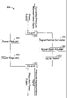
FIG. 5 illustrates one example of a signal-converting circuit 500. Signal
converting circuit 500 may, for example, be part of signal-converting circuit
board
150 (FIGs. 1A-B).
Circuit 500 includes a coupler 510, a power reducer 520, a power regulator
530, and a coupler 540. Coupler 510 receives a supply power and conveys a
converted signal that represents pressure. Coupler 510 may include one or more
connectors (e.g., pins) for receiving the supply power and conveying the
converted
14
CA 02576730 2007-02-02
WO 2006/026419
PCT/US2005/030385
pressure-representative signal. In particular implementations, the coupler may
receive
the supply power from and convey the converted pressure-representative signal
to an
external electrical connector. Power reducer 520 limits the supply power to a
specified range (e.g., 0-5 V). In particular implementations, power reducer
520 may
include a transistor for absorbing power in the supply power. The limited
signal is
conveyed to power regulator 530, which provides a reliably regulated supply
power.
In particular implementations, power regulator 530 may be a voltage regulator.
The
regulated signal is conveyed to coupler 540. Coupler 540 may have one or more
connectors (e.g., pins) for conveying the regulated supply power and receiving
a
pressure-representative signal. In particular implementations, the coupler may
convey
the regulated supply power to and receive the pressure-representative signal
from a
signal-conditioning circuit.
Circuit 500 also includes a signal biaser 550, a signal span adjuster 560, and
a
signal format converter 570. Signal biaser 550 is responsible for inserting an
offset
into the pressure-representative signal. For example, signal biaser 500 may
add a 5 V
offset to a signal. In particular implementations, the signal biaser may
provide the
offset through resistor dividers. Gain may then be applied to the offset
pressure-
representative signal by signal span adjuster 560. For example, signal span
adjuster
560 may double the span of the signal (e.g., from 5 V to 10 \T). In particular
implementations, signal span adjuster may include an amplifier. The scaled,
offset
pressure-representative signal may then be converted to another format by
format
converter 570. For example, a voltage may be converted to a current, a
frequency-
variable signal, a switched-output signal, a pulse-width modulated signal, a
pulse-
count signal, a digital signal, a wireless signal, or any other appropriate
format for
conveying information. The converted pressure-representative signal is then
conveyed out of circuit 500 by coupler 510.
Circuit 500 may be used to convert a pressure-representative signal of signal-
conditioning circuit board 150. In particular implementations, the pressure
representative signal is a 10%-90% of 5V ratiometric signal. Circuit 500 may
also be
used for converting signals of other systems, such as temperature measurement
systems, humidity measurement systems, or any other appropriate type of
transducer
CA 02576730 2007-02-02
WO 2006/026419
PCT/US2005/030385
system. In general, circuit 500 may be used for any appropriate type of
physical or
electrical variable measurement system.
Although FIG. 5 illustrates one implementation of a signal-converting circuit,
other implementations may include fewer, additional, and/or a different
arrangement
of components. For example, a signal-converting circuit may not include a
power
reducer and/or a power regulator, especially if the supply power is well-
regulated. As
another example, a signal-converting circuit may not include a signal biaser,
a signal
span adjuster, and/or a signal format converter, depending on the differences
between
the pressure-representative signal and the converted pressure-representative
signal.
For example, if a pressure-representative signal only needs to be biased, a
circuit may
not include a signal span adjuster or a signal format converter. In certain
implementations, however, unneeded components may be switched off or bypassed.
As a further example, the regulated supply power from power regulator 530 may
be
provided to other components of circuit 500, such as signal biaser 550 and
signal span
adjuster 560. As an additional example, various components of circuit 500 may
have
selectable characteristics. For example, signal biaser may be able to bias a
signal by
two or more amounts, and signal span adjuster may be able to scale a signal by
two or
more amounts.
FIG. 6 illustrates one example of a pressure-converting circuit 600. Circuit
600 is one implementation of pressure-converting circuit 500. Circuit 600 may
be
part of signal-converting circuit board 150 (FIGs. 1A-B).
In general, circuit 600 includes an input/output coupler 610, a circuit
protector
620, a voltage reducer 630, a voltage regulator 640, an input/output coupler
650, a
signal biaser 660, and a signal span adjuster 670. As discussed in more detail
below,
circuit 600 is designed to accept an unregulated voltage input from 9 to 36
Vdc,
although it may operate at up to 50 Vdc under limited conditions. The circuit,
however, can be readily modified to use other input voltage ranges (e.g., from
1 to
240 Vac or Vdc), with appropriate components. The circuit can also output a 0-
5 Vdc
signal or a 0-10 Vdc signal. In particular implementations, the circuit
operates at 5 V,
although other voltages (e.g., 4.096 V) are possible.
16
CA 02576730 2007-02-02
WO 2006/026419
PCT/US2005/030385
Input/output coupler 610 includes a connector 612 and conductors 614 (e.g.,
pins) that allow signals to be conveyed to and from circuit 600. In the
illustrated
implementation, an input supply voltage arrives on conductor 614a, and a
common
signal (e.g., ground) arrives on conductor 614c. Conductor 614b is used for
conveying the converted pressure-representative signal from the circuit. As
mentioned previously, the voltage through conductor 614a may be unregulated.
Circuit protector 620 is coupled to coupler 610 and protects circuit 600 from
improper signals, transient spikes, noise, and the like in the input supply
voltage. In
the illustrated implementation, circuit protector 620 includes a diode 622 and
a
capacitor 624. Diode 622 polarity protects the input supply voltage, and
capacitor
624 decouples the input supply voltage. In particular implementations, diode
622 is a
Schottkey diode, and capacitor 624 has a capacitance of 0.1 F.
To accommodate the voltage range of the input signal, voltage reducer 630
limits the input voltage to a predefined range (e.g., 0-5 V). The reduced
voltage is
conveyed to voltage regulator 640. Voltage reducer 630 includes a transistor
632,
which can absorb the bulk of the voltage. In particular implementations,
transistor
632 is an N-channel or a P-channel enhancement metal-oxide-semiconductor field-
effect transistor (MOSFET). Voltage reducer 630 also includes a resistor 634
and a
diode 636. Resistor 634 provides bias current to diode 636, which in turn
biases
transistor 632 on. In certain implementations, transistor 632 is biased into
linear
operation. Transistor 632 may be biased on by resistor 634 and diode 636 until
the
input to voltage regulator 640 is less than a given value (e.g., 2V) above the
output of
the voltage regulator. In particular implementations, diode 636 keeps the gate
of
transistor 632 biased at about 10 Vdc, which keeps the input to voltage
regulator 640
at about 8 V. In particular implementations, resistor 632 may have a
resistance of
100K Ohms, and diode 636 may be a zener diode.
Voltage regulator 640 produces a regulated supply voltage based on the supply
voltage from voltage reducer 630. Voltage regulator 640 includes a regulator
642 and
a capacitor 646. In the illustrated implementation, regulator 642 has five
input/output
connectors 644. The reduced voltage is received through connector 644a and fed
back through connector 644b. The regulated supply voltage, which may be quite
17
CA 02576730 2007-02-02
WO 2006/026419
PCT/US2005/030385
steady, is provided to input/output coupler 650 through connector 644e, which
is
coupled to a circuit rail 602. In particular implementations, regulator 640 is
a
precision 5 Vdc regulator able to source 5 mA, such as an LM4120 with 0.2%
accuracy and low thermal drift. Capacitor 646 provides stabilization and
decoupling
of the output signal. Capacitor 646 may have a capacitance of 0.022 F.
Input/output coupler 650 is coupled to voltage regulator 640 through rail 602
and includes connector 654 and conductors 654. Input/output coupler 650
provides
the regulated voltage to a signal-conditioning circuit board through conductor
654a.
This signal may excite that circuit board so that is may generate a signal
representative of pressure. The pressure-representative signal is received
through
conductor 654b. In particular implementations, the pressure-representative
signal is
expected to be linear over 10% to 90 % of the span (e.g., 0.5-4.5 V) for a 0-5
V
signal.
Signal biaser 660 is also coupled to rail 602 and includes a voltage divider
662
that divides the rail to provide a reference voltage for the output stage
(e.g., signal
span adjuster 670). This reference voltage is ratiometric to the rail. In
doing so,
voltage divider 662 sets the offset for the pressure-representative signal
received
through connector 654b of input/output coupler 650.
In this implementation, voltage divider 662 includes thermal-coefficient-
matched resistors 663. In particular implementations, resistor 663a may have a
resistance of 453K Ohms, and resistor 663b may have a resistance of 90.9K
Ohms.
Resistors 663 may be precise (e.g., 0.1% deviation and 25 ppm thermal drift),
although they need not be.
Signal biaser 660 also includes offset selector 664. Offset selector 664
allows
the offset of signal biaser 660 to be selected. As illustrated, offset
selector 664
includes a resistor 665 and a switch 666. In particular implementations,
resistor 665
may have a resistance of 75K Ohms. When switch 666 is open, signal biaser 660
may
bias the signal 2.5 V. When switch 666 is closed, resistor 665 may be viewed
as part
of the voltage divider 662. Closing switch 666 may set the output voltage to 0
Vdc
when the input is equal to 10% of 5 V.
18
CA 02576730 2007-02-02
WO 2006/026419
PCT/US2005/030385
Signal biaser 660 additionally includes a buffer 668, which buffers the offset
voltage. Buffer 668 includes an operational amplifier 669, which, in
particular
implementations, may be a TS27L2AID. Operational amplifier 669 acts as a
voltage-
follower to buffer voltage divider 662, including when the parallel value of
resistor
663b is included when switch 666 is closed.
Signal span adjuster 670 is coupled to coupler 650 and receives the pressure-
representative signal received through conductor 654b. Signal span adjuster
670
scales the pressure-representative signal to the appropriate range (e.g., from
5V to 10
V). In the illustrated implementation, signal span adjuster 670 acts as a
differential
amplifier that compares the pressure-representative signal voltage to a stable
reference
voltage and provides precise differential gain with a single-ended (ground
referenced)
output voltage.
Signal span adjuster 670 includes a voltage divider 672, an operational
amplifier 674, and a switch 676. Voltage divider 672 includes thermal-
coefficient-
matched resistors 673. Resistors 673 may be matched by a variety of
techniques. In
particular implementations, each of resistors 673 has a resistance of 150K
Ohms. In
this implementation, when switch 6076 is open, signal span adjuster 670
behaves as a
normal-mode amplifier (non-inverting, in particular), and when switch 676 is
closed,
signal span adjuster 670 behaves as a differential amplifier. In certain
implementations, signal span adjuster 670 doubles the span of the signal.
The output of signal span adjuster 670 is fed back through another voltage
divider 678, which also receives the output of buffer 668. Voltage divider 678
includes thermal-coefficient-matched resistors 679. In particular
implementations,
each of resistors 679 has a resistance of 150K Ohms. The thermal-coefficients
of
resistors 679 do not have to correspond to that of resistors 673. Voltage
divider 678
forces the voltage of operational amplifier 674 to follow a non-zero voltage
offset that
when combined with the span adjustment, places the output at 0 V when the
input is at
0.5V.
In one mode of operation, circuit 600 produces a 0-5 V output signal when
switch 666 and switch 676 are closed. With the voltage signal received through
conductor 654b at 0.5 Vdc, voltage divider 672, with 150K Ohm resistors, sets
the
19
CA 02576730 2007-02-02
WO 2006/026419
PCT/US2005/030385
non-inverting input of operational amplifier 674 to 0.250 Vdc. The output of
operational amplifier 669 is a buffered voltage set by voltage divider 662
from rail
602, which is at +5 V. The buffered voltage is then 0.416 Vdc with switch 666
closed,
and the parallel combination of resistor 677 and resistor 679b is 100K Ohms
(i.e.,
(300*150)/(300+150)). For the following formulas, this will be expressed as
resistor
679a'. The output formula is as follows:
Vout = Vin/(R673a+R673b)*R673b*(1+(R679b/R679a'))-
(Voffset*(R679b/R679a')),
where R is the resistance of the associated resistor, and Vout is the output
of
operational amplifier 674. For the mentioned implementation, this translates
to:
Vout = Vin/(150+150)*150*(1+(150/100))-(0.416*(150/100)).
Thus,
Vout = 0.001 Vdc with Vin= 0.5 Vdc; and
Vout = 5.001 Vdc with Vin = 4.5 Vdc.
To change the circuit for a 0-10 Vdc output, switch 666 and switch 676 are
opened. Opening switch 676 changes the circuit to a follower with an offset.
This
effectively eliminates voltage divider 672. To compensate for the change in
the offset,
switch 666 is also opened, which changes the buffered offset to 0.835Vdc.
Now, the output formula may be expressed as:
Vout = Vin*(1+(R679b/R679a'))-( R679b/R679a')*Voffset.
With the mentioned implementation, this produces:
Vout = Vin*(1+(150/100))-(150/100)*0.835;
Vout = -0.002 Vdc, with Vin= 0.5 Vdc; and
Vout = 9.998 Vdc, with Vin = 4.5 Vdc
Circuit 600, therefore, may convert a ratiometric input voltage from an
external device (e.g., signal-conditioning circuit board 130) to an output of
0-5 Vdc or
0-10 Vdc.
CA 02576730 2007-02-02
WO 2006/026419
PCT/US2005/030385
In order for operational amplifier 674 to swing to (or through) zero volts, it
may be necessary to generate a slightly negative internal supply rail. This
may be
achieved by voltage regulator 680. Voltage regulator 680 includes a regulator
682
and a capacitor 684, which produce the negative voltage. Regulator 682 may,
for
example, be a charge-pump voltage inverter. A capacitor 686 filters the
resultant -5
Vdc. Capacitor 684 and capacitor 686 may each have a capacitance of 1 F.
In particular implementations, circuit 600 may include one or more transient
voltage suppressors, blocking diodes, chokes, and decoupling capacitors, to
protect
from mis-wiring and short circuits, provide output current limiting, block
transient
signal spikes, and minimize EMI, ESD, and transient noise. In particular
implementations, the output voltage may be finished off with a compound
transistor
totem circuit that provides wider output swing, with short-circuit protection,
output
current limiting, mis-wiring protection, and increased capacitive drive
capability.
In one mode of operation, the output received from the signal-conditioning
circuit board is expected to be linear over a range (e.g., from 10% of the
regulated
voltage (at zero pressure) to 90% of the regulated voltage (at full-scale
pressure)).
Thus, with the circuit gain fixed, the span accuracy is dependent on the fixed
gain of
the circuit and the regulation of the voltage on rail 602. The output accuracy
is
determined, at least in part, by the offset of circuit 600. Thus, precision
resistors may
be used for setting the offset stage of the circuit. Output offset thermal
performance
may be determined by the thermal-coefficient matching of the offset resistors
and
input offsets of the operational amplifiers. Output span thermal performance
may be
determined by the thermal-coefficient matching of the gain resistors, as well
as the
thermal drift of voltage regulator 640.
In certain implementations, the regulated voltage may be matched to the
nominal driver-circuit voltage in the signal-conditioning circuit. For
example, if the
nominal driver-circuit voltage in the signal-conditioning circuit is 5 V, the
regulated
voltage may be 5 Vdc. However, any other appropriate voltage may be used. For
instance, using 4.096 V may provide the advantage of reducing the driver
circuit's
current demand, which may be important in operating at less than 4 mA for a 4-
20
mA, two-wire output.
21
CA 02576730 2007-02-02
WO 2006/026419
PCT/US2005/030385
In order to maintain consistent offset and offset thermal coefficients, the
tolerances and thermal-coefficients of the offset resistors may be tightly
controlled,
and possibly even matched. In particular implementations, matching is not
necessary,
so long as the tolerances are within 0.1%, and the thermal-coefficient of
resistance are
within 25 ppm.
In order to maintain consistent span and span thermal coefficients, the
tolerance and thermal-coefficients of the gain setting resistors may be
controlled. In
particular implementations, resistor networks (pairs) with 50 ppm tolerances
and 5
ppm matched thermal-coefficient resistors may be used.
Although one implementation of circuit 600 has been discussed, other
implementations are possible. One approach may be to use thick-film or thin-
film
printed resistors (on a ceramic substrate or on a hybrid with the active
components
mounted), because printed resistors have matched thermal coefficients of
resistance.
If necessary, the same resistors could be laser-trimmed or abrasive-trimmed by
the
board manufacturer to calibrate gain and offset. Another approach may be to
use
digitally-trimmed potentiometers to set the offset and gain. Although
digitally-
trimmed potentiometers typically have high end-to-end thermal coefficients of
resistance, if used in the potentiometric mode, they tend to have well-matched
thermal-coefficients of resistance, so the thermal effects may be low.
Drawbacks to
this approach include relatively high cost, low resolution, and relatively
large size, but
these are expected to improve in the future. Also, digitally-controlled
digital-to-
analog converters (DACs) could be used for the same purpose.
Circuit 600 has a variety of features. For example, circuit 600 can limit a
variable input voltage to a predefined voltage (e.g., 5 Vdc). Reducing the
voltage
supplied to the voltage regulator reduces the amount of power dissipated by
the
voltage regulator, which reduces its internal temperature and, therefore,
thermal effect
(e.g., error generation). Also, this extends the input voltage range of the
circuit and
allows a higher voltage to be input than the voltage regulator can normally
handle.
Moreover, the regulated voltage may be supplied to a detector circuit (e.g.,
signal-
conditioning circuit board 130). As another example, circuit 600 can supply
two
different output signals (e.g., one between 0-5 V and one between 0-10 V).
Thus,
22
CA 02576730 2007-02-02
WO 2006/026419
PCT/US2005/030385
circuit 600 can satisfy two operational constraints. As an additional example,
circuit
600 can produce an output signal that is proportional with a 10%-90% 5V
ratiometric
signal without adding significant offset error, gain error, offset thermal
error, or gain
thermal error. For example, in particular implementations, changes to output
values
may be less than 0.40% of the input/output range within a temperature range of-
20-
85 C. Moreover, circuit 600 may be a fixed, precise transfer function with no
trimming required on installation.
FIG. 7 illustrates a pressure-converting circuit 700. Circuit 700 is one
implementation of pressure-converting circuit 500. Circuit 700 may be part of
signal-
converting circuit board 150.
In general, circuit 700 includes an input/output coupler 710, a circuit
protector
720, a voltage reducer 730, a voltage regulator 740, an input/output coupler
750, a
signal biaser 760, and a signal span adjuster 770. These components may be
similar
to those for circuit 600. As discussed in more detail below, circuit 700 is
designed to
accept an unregulated voltage input from 9 to 36 Vdc, although it may operate
at up to
50 Vdc under limited conditions. The circuit, however, can be readily modified
to use
other input voltage ranges (e.g., from 1 to 240 Vac or Vdc), with appropriate
components. The circuit can also output a 1-5 Vdc signal or a 1-6 Vdc signal.
In
particular implementations, the circuit operates at 5 V, which may be supplied
to
other circuits, although other voltages (e.g., 4.096 V) are possible.
Input/output coupler 710 includes a connector 712 and conductors 714 (e.g.,
pins) that allow signals to be conveyed to and from circuit 700. In the
illustrated
implementation, an input supply voltage arrives on conductor 714a, and a
common
signal (e.g., ground) arrives on conductor 714c. Conductor 714b is used for
conveying the converted pressure-representative signal from the circuit.
Circuit protector 720 is coupled to input/output coupler 710 and protects
circuit 700 from improper signals, transient spikes, noise, and the like in
the input
supply voltage. In the illustrated implementation, circuit protector 720
includes a
diode 722 and a capacitor 724. Diode 722 polarity protects the input supply
voltage,
and capacitor 724 decouples the input supply voltage.
23
CA 02576730 2007-02-02
WO 2006/026419
PCT/US2005/030385
To accommodate the voltage range of the input signal, voltage reducer 730
limits the input voltage to a predefined range (e.g., 0-5 V). The reduced
voltage is
conveyed to voltage regulator 740. Voltage reducer 730 includes a transistor
732,
which can absorb the bulk of the voltage. Voltage reducer 730 also includes a
resistor
734 and a diode 736. Resistor 734 provides bias current to diode 736, which in
turn
biases transistor 732 on. In certain implementations, transistor 732 is biased
into
linear operation. Transistor 732 may be biased on by resistor 734 and diode
736 until
the input to voltage regulator 740 is less than a given value (e.g., 2V) above
the output
of the voltage regulator. In particular implementations, diode 736 keeps the
gate of
transistor 732 biased at about 10 Vdc, which keeps the input to voltage
regulator 740
at about 8 V.
Voltage regulator 740 produces a regulated supply voltage based on the supply
voltage from voltage reducer 730. Voltage regulator 740 includes a regulator
742 and
a capacitor 746. In the illustrated implementation, regulator 742 has five
input/output
connectors 744. The reduced voltage is received through connector 744a and fed
back through connector 744b. The regulated supply voltage, which may be quite
steady, is provided to input/output coupler 750 through connector 744e, which
is
coupled to a circuit rail 702. Capacitor 746 provides stabilization and
decoupling of
the regulated output signal.
Input/output coupler 750 is coupled to voltage regulator 740 through rail 702
and includes connector 754 and conductors 754. Input/output coupler 750
provides
the regulated supply voltage to a signal-conditioning circuit board through
conductor
754a. This signal may excite that circuit board so that it may generate a
signal
representative of pressure. The pressure-representative signal is received
through
conductor 754b.
Signal biaser 760 is also coupled to rail 702 and includes a voltage divider
762
that divides the rail to provide a reference voltage for the output stage
(e.g., signal
span adjuster 770). This reference voltage is ratiometric to the rail. In
doing so,
voltage divider 762 sets the offset for the pressure-representative signal
received
through connector 754b of input/output coupler 750.
24
CA 02576730 2007-02-02
WO 2006/026419 PCT/US2005/030385
In this implementation, voltage divider 762 includes thermal-coefficient-
matched resistors 763. In particular implementations, resistor 763a may have a
resistance of 332K Ohms, and resistor 763b may have a resistance of 60.4K
Ohms.
Resistors 763 may be precise (e.g., 0.1% deviation and 25 ppm thermal drift),
although they need not be.
Signal biaser 760 also includes a buffer 768, which buffers the offset
voltage.
Buffer 768 includes an operational amplifier 769. Operational amplifier 769
acts as a
voltage-follower to buffer voltage divider 762.
Signal span adjuster 770 is coupled to coupler 750 and receives the pressure-
representative signal received through conductor 754b. Signal span adjuster
770
scales the pressure-representative signal to the appropriate range (e.g., from
5V to 6 .
V). In the illustrated implementation, signal span adjuster 770 acts as a
differential
amplifier that compares the pressure-representative signal voltage to a stable
reference
voltage and provides precise differential gain with a single-ended (ground
referenced)
output voltage.
Signal span adjuster 700 includes a voltage divider 772, an operational
amplifier 774, and a diode 775. Voltage divider 772 includes thermal-
coefficient-
matched resistors 773. In particular implementations, each of resistors 773
has a
resistance of 150K Ohms. Diode 775 provides a bandgap voltage reference, which
may allow a calibrated voltage to be maintained regardless of input current.
Diode
775 may provide a 1.2 Vdc reference with low thermal error and good precision.
In
particular implementations, diode 775 is implemented as an integrated circuit
that
behaves as a perfect zener diode.
Signal span adjuster 770 also includes a switch 776, a voltage divider 777,
and
a resistor 779. The output of signal span adjuster 770 is fed back through
voltage
divider 777, which also receives the output of buffer 768. Voltage divider 777
includes thermal-coefficient-matched resistors 778. In particular
implementations,
each of resistors 778 has a resistance of 150K Ohms. Voltage divider 777
forces the
voltage of operational amplifier 774 to follow a non-zero voltage offset that
when
combined with the span adjustment, places the output at 1 V when the input is
at
0.5V.
CA 02576730 2007-02-02
WO 2006/026419
PCT/US2005/030385
In one mode of operation, circuit 700 produces a 1-5 V output signal when
switch 776 is open. With the voltage signal received through conductor 754b at
0.5
Vdc, voltage divider 772, with 150K Ohm resistors, sets the non-inverting
input of
operational amplifier 774 to 0.8625 Vdc. Resistor 779 biases diode 775 on. The
output of operational amplifier 769 is a buffered voltage set by voltage
divider 762
from rail 702, which is at +5 V. The buffered voltage is therefore 0.77 Vdc,
with
resistor 763a having a resistance of 332K Ohms and resistor 763b having a
resistance
of 60.3 Ohms. The output formula may be expressed as follows:
Vout = (1.225V-(1.225-Vin)/(R773a+R773b)*R773b)+(((1.225V-(1.225V-
Vin)/(R773a+R773b)*R773b)-0.77)/R778a*R778b).
For the mentioned implementation, this translates to:
Vout = (1.225V-(1.225-Vin)/(150+150)*150)+(((1.225V-(1.225V-
Vin)/(150+150)*150)-0.77)/150*150)
Thus, with the input to voltage divider 772 at 0.5 Vdc (at zero pressure), the
output of operational amplifier 774 will be 0.955 Vdc. This deviation can be
altered
(e.g., with a second switch), but in certain implementations, a fixed offset
adjustment
is considered acceptable. With the input at 4.5 Vdc, voltage divider 772 sets
the non-
inverting input of operational amplifier 774 to 2.8625 V. Therefore, the
output of
operational amplifier 774 will be 2.8625V+(2.8625 Vdc - 0.77 Vdc), or 4.955
Vdc
(for a span of 4.000 Vdc).
To change the circuit for a 1-6 Vdc output, switch 776 is closed. Closing
switch 776 changes the ratio of voltage divider 777 and causes signal span
adjuster
770 to increase the span of the signal by 20%. The offset voltages may be
optimized
for this gain. The parallel combination of resistor 778a and resistor 779 is
100K
Ohms (i.e., (300*150)/(300+150)). For the following formulas, this will be
expressed
as resistor 778a'. Now, the output formula may be expressed as:
Vout = (1.225V-(1.225-Vin)/(R773a+R773b)*R773b)+(((1.225V-(1.225V-
Vin)/(R773a+R773b)*R773b)-0.77)/R778a'*R778b)
With the mentioned implementation, this produces:
26
CA 02576730 2007-02-02
WO 2006/026419
PCT/US2005/030385
Vout = (1.225V-(1.225-Vin)/(150+150)*150)+(((1.225V-(1.225V-
Vin)/(150+150)*150)-0.77)/100*150);
Vout = 1.001 Vdc with Vin= 0.5 Vdc; and
Vout = 6.001 Vdc with Vin = 4.5 Vdc.
Circuit 700, therefore, may convert a ratiometric input voltage from an
external device (e.g., signal-conditioning circuit board 130) to an output of
1-5 Vdc or
1-6 Vdc.
Circuit 700 has a variety of features. For example, circuit 700 can limit a
variable input voltage to a predefined voltage (e.g., 5 Vdc). Reducing the
voltage
supplied to the voltage regulator reduces the amount of power dissipated by
the
voltage regulator, which reduces its internal temperature and, therefore,
thermal effect
(e.g., error generation). Also, this extends the input voltage range of the
circuit and
allows a higher voltage to be input than the voltage regulator can normally
handle.
Moreover, the regulated voltage may be supplied to a detector circuit (e.g.,
signal-
conditioning circuit board 130). As another example, circuit 700 can supply
two
different output signals (e.g., one between 1-5 V and one between 1-6 V).
Thus,
circuit 700 can satisfy two operational constraints. As an additional example,
circuit
700 can signal condition a 10%-90% 5V ratiometric signal without adding
significant
offset error, gain error, or thermal offset or gain errors. Moreover, circuit
700 may be
a fixed, precise transfer function with no trimming required on installation.
FIG. 8 illustrates a pressure-converting circuit 800. Circuit 800 is one
implementation of pressure-converting circuit 500. Circuit 800 may be part of
signal-
converting circuit board 150.
In general, circuit 800 includes an input/output coupler 810, a circuit
protector
820, a voltage reducer 830, a voltage regulator 840, an input/output coupler
850, a
signal biaser 860, and a signal span adjuster 870. These components may be
similar
to those for circuit 600. Circuit 800 also includes a signal format converter
880. As
discussed in more detail below, circuit 800 is designed to accept an
unregulated
voltage input from 9 to 36 Vdc, although it may operate at up to 50 Vdc under
limited
conditions. The circuit, however, can be readily modified to use other input
voltage
27
CA 02576730 2007-02-02
WO 2006/026419
PCT/US2005/030385
ranges (e.g., from 1 to 240 Vac or Vdc), with appropriate components. The
circuit
can also output a 4-20 mA signal, which can be drawn through the voltage
input. In
particular implementations, the circuit operates at 5 V, which may be supplied
to
other circuits, although other voltages (e.g., 4.096 V) are possible.
Input/output coupler 810 includes a connector 812 and conductors 814 (e.g.,
pins) that allow signals to be conveyed to and from circuit 800. In the
illustrated
implementation, an input supply voltage arrives on conductor 814a, and a
common
signal (e.g., ground) arrives on conductor 814b, to which conductor 814c is
tied.
Conductor 814 is used for conveying the converted pressure-representative
signal
from the circuit.
Circuit protector 820 is coupled to input/output coupler 810 and protects
circuit 800 from improper signals, transient spikes, noise, and the like in
the input
supply voltage. In the illustrated implementation, circuit protector 820
includes a
diode 822 and a capacitor 824. Diode 822 polarity protects the input supply
voltage,
and capacitor 824 decouples the input supply voltage.
To accommodate the voltage range of the input signal, voltage reducer 830
limits the input voltage to a predefined range (e.g., 0-5 V). The reduced
voltage is
conveyed to voltage regulator 840. Voltage reducer 830 includes a transistor
832,
which can absorb the bulk of the voltage. Voltage reducer 830 also includes a
resistor
834 and a diode 836. Resistor 834 provides bias current to diode 836, which in
turn
biases transistor 832 on. In certain implementations, transistor 832 is biased
into
linear operation. Transistor 832 may be biased on by resistor 834 and diode
836 until
the input to voltage regulator 840 is less than a given value (e.g., 2V) above
the output
of the voltage regulator. In particular implementations, diode 836 keeps the
gate of
transistor 832 biased at about 10 Vdc, which keeps the input to voltage
regulator 840
at about 8 V.
Voltage regulator 840 produces a regulated supply voltage based on the supply
voltage from voltage reducer 830. Voltage regulator 840 includes a regulator
842 and
a capacitor 846. In the illustrated implementation, regulator 842 has five
input/output
connectors 844. The reduced supply voltage is received through connector 844a
and
fed back through connector 844b. The regulated supply voltage, which may be
quite
28
CA 02576730 2007-02-02
WO 2006/026419
PCT/US2005/030385
steady, is provided to input/output coupler 850 through connector 844e, which
is
coupled to a circuit rail 802. Capacitor 846 provides stabilization and
decoupling of
the regulated output signal.
Input/output coupler 850 is coupled to voltage regulator 840 through rail 802
and includes connector 852 and conductors 854. Input/output coupler 850
provides
the regulated supply voltage to a signal-conditioning circuit board through
conductor
854a. This signal may excite that circuit board so that it may generate a
signal
representative of pressure. The pressure-representative signal is received
through
conductor 854b.
Signal biaser 860 is also coupled to rail 802 and includes a voltage divider
862
that divides the rail to provide a reference voltage for the transconductance
stage (e.g.,
signal span adjuster 870 and signal format converter 880). This reference
voltage is
ratiometric to the rail. In doing so, voltage divider 862 sets the offset for
the pressure-
representative signal received through connector 854b of input/output coupler
850.
In this implementation, voltage divider 862 includes thermal-coefficient-
matched resistors 863. In particular implementations, resistor 863a may have a
resistance of 200K Ohms, and resistor 863b may have a resistance of 300K Ohms.
Resistors 863 may be precise (e.g., 0.1% deviation and 25 ppm thermal drift),
although they need not be.
Signal biaser 860 also includes a buffer 868, which buffers the offset
voltage.
Buffer 868 includes an operational amplifier 869. Operational amplifier 869
acts as a
voltage-follower to buffer voltage divider 862.
Signal span adjuster 870 is coupled to coupler 850 and receives the pressure-
representative signal received through conductor 854b. Signal span adjuster
870
scales the pressure-representative signal to the appropriate range (e.g., from
4 mA to
16 mA). In the illustrated implementation, signal span adjuster 870 acts as a
differential amplifier that compares the pressure-representative signal
voltage to a
stable reference voltage and provides precise differential gain with a single-
ended
(ground referenced) output voltage.
29
CA 02576730 2007-02-02
WO 2006/026419
PCT/US2005/030385
Signal span adjuster 870 includes a voltage divider 872, an operational
amplifier 874, a resistor 875, and a resistor 876. Voltage divider 872
includes
thermal-coefficient-matched resistors 873. In particular implementations,
resistor
873a has a resistance of 100K Ohms, and resistor 873b has a resistance of 20K
Ohms.
Resistor 875 and resistor 876 are coupled to rail 802 and facilitate supplying
a
minimum output current. In particular implementations, resistor 875 may have a
resistance of 1.91K Ohms, and resistor 876 may have a resistance of 127K Ohms.
In
certain implementations, resistor 876 may be precision resistor, which may
mask non-
precision of resistor 875.
Signal span adjuster 870 also includes a voltage divider 877. The output of
signal format converter 880 is fed back through voltage divider 877, which
also
receives the output of buffer 868. Thus, the output of operational amplifier
869 is
divided by voltage divider 877 and summed to the inverting input of
operational
amplifier 874. Voltage divider 877 includes thermal-coefficient-matched
resistors
878. In particular implementations, resistor 878a has a resistance of 100K
Ohms, and
resistor 878b has a resistance of 20K Ohms. Voltage divider 877 forces the
voltage of
operational amplifier 874 to follow a non-zero voltage offset that when
combined
with the span adjustment, placing the output at 1 V when the input is at 0.5V.
Signal format converter 880 is coupled to signal span adjuster 870. Signal
format converter 880 includes a resistor 882, a transistor 884, a resistor
885, and a
resistor 886. Resistor 882 limits current to the base of transistor 884,
resistor 885 is a
current limiting resistor to limit the maximum output signal, and resistor 886
operates
as a current sense resistor. That is, resistor 886 is the current-sensing
feedback
element. The voltage across resistor 886 is proportional to the total circuit
current,
which is the output signal itself, and the voltage is fed back to operational
amplifier
874. The performance accuracy of circuit 600 is also affected by the resistor
886.
Operational amplifier 874 provides a differential gain to develop a voltage
across
resistor 886, by driving transistor 884, which may be an NPN power transistor,
to
induce a controlled current into the common signal. In particular
implementations,
resistor 882 has a resistance of 4.99K Ohms, resistor 884 has a resistance of
10 Ohms,
CA 02576730 2007-02-02
WO 2006/026419
PCT/US2005/030385
and resistor 886 has a resistance of 50 Ohms. In certain implementations,
resistor 886
may be implemented as a pair of parallel resistors, which may reduce
variability.
Signal format converter 880 also includes a capacitor 887 and a capacitor 888.
Capacitor 887 stabilizes operational amplifier 874 by reducing gain at higher
frequencies. Capacitor 888 rolls off the frequency response of circuit 800. In
particular implementations, capacitor 887 has a capacitance of 0.01 tF, and
capacitor
888 has a capacitance of 0.1 1A,F.
In one mode of operation, the output of operational amplifier 869 is divided
by
voltage divider 877 and summed to the inverting input of operational amplifier
874 to
set the inverting input to the operational amplifier to 0.5 Vdc. Thus, with
the input at
voltage divider 872 at 0.5 Vdc (at zero pressure), no current flows through
voltage
divider. Resistor 875 and resistor 876, however, drive enough current into
resistor
873b to induce a 4 mA total current draw, which is accomplished by operational
amplifier 874 biasing transistor 884 on enough to maintain an input balance at
0.5
Vdc. As the input voltage is raised to 4.5 Vdc, operational amplifier 874,
transistor
882, and resistor 886 cooperate to maintain the non-inverting input at 0.5
Vdc. At full
scale, input signal at 4.5 Vdc, this equates to dropping 4 Vdc (4.5 Vdc - 0.5
Vdc)
across resistor 873b, which produces 20 mA if resistor 873b has a resistance
of 20K
Ohms.
Circuit 800, therefore, may convert a ratiometric input voltage from an
external device (e.g., signal-conditioning circuit board 130) to an output of
4-20 mA.
Circuit 800 has a variety of features. For example, circuit 800 can limit a
variable input voltage to a predefined voltage (e.g., 5 Vdc). Reducing the
voltage
supplied to the voltage regulator reduces the amount of power dissipated by
the
voltage regulator, which reduces its internal temperature and, therefore,
thermal effect
(e.g., error generation). Also, this extends the input voltage range of the
circuit and
allows a higher voltage to be input than the voltage regulator can normally
handle.
Moreover, the regulated voltage may be supplied to a detector circuit (e.g.,
signal-
conditioning circuit board 130).
31
CA 02576730 2007-02-02
WO 2006/026419
PCT/US2005/030385
As another example, the circuit may have low thermal self-heating of a 4-20
mA output, due to intrinsically low thermal-coefficients by design. 4-20mA
devices
by nature create heat, which causes self-heating errors in pressure sensor
assemblies.
As the design of these assemblies get smaller, this problem typically worsens.
But
with circuit 800, the heat generated may have little effect on itself because
only low-
thermal effect components are used. The benefit is that the whole assembly has
low
self-heating effect, and it is easier to keep the heat from the heat-sensitive
parts (e.g.,
the signal-conditioning circuit and the pressure detector).
As an additional example, circuit 800 may convert the format of a signal,
which assists in meeting operational constraints. As a further example,
circuit 800
can signal condition a 10%-90% 5V ratiometric signal without adding
significant
offset error, gain error, or thermal offset or gain errors. Moreover, circuit
800 may be
a fixed, precise transfer function with no trimming required on installation.
FIG. 9 illustrates a pressure-converting circuit 900. Circuit 900 is one
implementation of pressure-converting circuit 500. Circuit 900 may be part of
signal-
converting circuit board 150.
In general, circuit 900 includes an input/output coupler 910, a circuit
protector
920, a voltage reducer 930, a voltage regulator 940, an input/output coupler
950, a
signal biaser 960, and a signal span adjuster 970. As discussed in more detail
below,
circuit 900 is designed to accept an unregulated voltage input from 9 to 36
Vdc,
although it may operate at up to 50 Vdc under limited conditions. The circuit,
however, can be readily modified to use other input voltage ranges (e.g., from
1 to
240 Vac or Vdc), with appropriate components. The circuit can also output a 0-
5 Vdc
signal or a 0-10 Vdc signal. In particular implementations, the circuit
operates at 5 V,
although other voltages (e.g., 4.096 V) are possible.
Input/output coupler 910 includes a connector 912 and conductors 914 (e.g.,
pins) that allow signals to be conveyed to and from circuit 900. In the
illustrated
implementation, an input supply voltage arrives on conductor 914a, and a
common
signal (e.g., ground) arrives on conductor 914c. Conductor 914b is used for
conveying the converted pressure-representative signal from the circuit.
32
CA 02576730 2007-02-02
WO 2006/026419
PCT/US2005/030385
Circuit protector 920 is coupled to coupler 910 and protects circuit 900 from
improper signals, transient spikes, noise, and the like in the input supply
voltage. In
the illustrated implementation, circuit protector 920 includes a diode 922 and
a
capacitor 924. Diode 922 polarity protects the input supply voltage, and
capacitor
924 decouples the input supply voltage.
To accommodate the voltage range of the input signal, voltage reducer 930
limits the input voltage to a predefined range (e.g., 0-5 V). The reduced
voltage is
conveyed to voltage regulator 940. Voltage reducer 930 includes a transistor
932,
which can absorb the bulk of the voltage. Voltage reducer 930 also includes a
resistor
934 and a diode 936. Resistor 934 provides bias current to diode 936, which in
turn
biases transistor 932 on. In certain implementations, transistor 932 is biased
into
linear operation. Transistor 932 may be biased on by resistor 934 and diode
936 until
the input to voltage regulator 940 is less than a given value (e.g., 2 V)
above the
output of the voltage regulator. In particular implementations, diode 936
keeps the
gate of transistor 932 biased at about 10 Vdc, which keeps the input to
voltage
regulator 940 at about 8 V.
Voltage regulator 940 produces a regulated supply voltage based on the supply
voltage from voltage reducer 930. Voltage regulator 940 includes a regulator
942 and
a capacitor 946. In the illustrated implementation, regulator 942 has five
input/output
connectors 944. The reduced voltage is received through connector 944a and fed
back through connector 944b. The regulated supply voltage, which may be quite
steady, is provided to input/output coupler 950 through connector 944e, which
is
coupled to a circuit rail 902. Capacitor 946 provides stabilization and
decoupling of
the output signal.
Input/output coupler 950 is coupled to voltage regulator 940 through rail 902
and includes connector 952 and conductors 954. Input/output coupler 950
provides
the regulated voltage to a signal-conditioning circuit board through conductor
954a.
This signal may excite that circuit board so that is may generate a signal
representative of pressure. The pressure-representative signal is received
through
conductor 954b. In particular implementations, the pressure-representative
signal is
33
CA 02576730 2007-02-02
WO 2006/026419
PCT/US2005/030385
expected to be linear over 10% to 90 % of the span (e.g., 0.5-4.5 V) for a 0-5
V
signal.
Signal biaser 960 is also coupled to rail 902 and includes a voltage divider
962
that divides the rail to provide a reference voltage for the output stage
(e.g., signal
span adjuster 970). This reference voltage is ratiometric to the rail. In
doing so,
voltage divider 962 sets the offset for the pressure-representative signal
received
through connector 954b of input/output coupler 950.
In this implementation, voltage divider 962 includes thermal-coefficient-
matched resistors 963. In particular implementations, resistor 963a may have a
resistance of 100K Ohms, and resistor 963b may have a resistance of 11K Ohms.
Resistors 963 may be precise (e.g., 0.1% deviation and 25 ppm thermal drift),
although they need not be.
Signal biaser 960 additionally includes a buffer 968, which buffers the offset
voltage. Buffer 968 includes an operational amplifier 969. Operational
amplifier 969
acts as a voltage-follower to buffer voltage divider 962.
Signal span adjuster 970 is coupled to coupler 950 and receives the pressure-
representative signal received through conductor 954b. Signal span adjuster
970
scales the pressure-representative signal to the appropriate range (e.g., from
5V to 10
V). In the illustrated implementation, signal span adjuster 970 acts as a
differential
amplifier that compares the pressure-representative signal voltage to a stable
reference
voltage and provides precise differential gain with a single-ended (ground
referenced)
output voltage.
Signal span adjuster 970 includes a voltage divider 971, a switch 973, and an
operational amplifier 974. Voltage divider 971 includes thermal-coefficient-
matched
resistors 972. In particular implementations, resistor 972a has a resistance
of 40K
Ohms, resistor 972b has a resistance of 50K Ohms, and resistor 972c has a
resistance
of 40K Ohms.
The output of signal span adjuster 970 is fed back through another voltage
divider 976, which also receives the output of buffer 968. Voltage divider 976
includes thermal-coefficient-matched resistors 977. In particular
implementations,
34
CA 02576730 2007-02-02
WO 2006/026419
PCT/US2005/030385
resistor 977a has a resistance of 40K Ohms, resistor 977b has a resistance of
50K
Ohms, and resistor 977c has a resistance of 40K Ohms. Voltage divider 976
forces
the voltage of operational amplifier 974 to follow a non-zero voltage offset
that when
combined with the span adjustment, places the output at 0 V when the input is
at
0.5V.
Signal span adjuster 970 also includes a switch 978. In particular
implementations, switch 973 and switch 978 allow gain to be modified in a
balanced
way on the differential and feedback sides.
In one mode of operation, circuit 900 produces a 0-5 V output signal when
switch 973 and switch 978 are open. With the voltage signal received through
conductor 954b at 0.5 Vdc, voltage divider 971, with the previously mentioned
resistances, sets the non-inverting input of operational amplifier 974 to 0.5
Vdc. The
output of operational amplifier 969 is a buffered voltage set by voltage
divider 962
from rail 902, which is at +5 V. The buffered voltage is then 0.5 Vdc, which
results
in the differential between Vin and Voffset being 0 Vdc when the pressure-
representative signal is at 0.5 Vdc. The output is the gain multiplied times
the
difference between the Vin and Voffset voltage.
Assuming that voltage dividers 971 and 976 use matched resistance values, the
output may be expressed as follows:
Vout = (Vin-Voffset)*(R977b/R977a)).
Thus, for the mentioned implementation:
Vout = (Vin-0.5 Vdc)*(50/40);
Vout = 0.000 Vdc with Vin = 0.5 Vdc; and
Vout = 5.000 Vdc with Vin = 4.5 Vdc.
To change circuit 900 for a 0-10 Vdc output, switch 973 and switch 978 are
closed. Placing resistor 972c in parallel with resistor 972a changes the ratio
of
voltage divider 971 from 50/40 to 50/20. The same is true for voltage divider
976.
Therefore, the output may be expressed as:
Vout = (Vin-Voffset)*(R977b/R977a'))
CA 02576730 2007-02-02
WO 2006/026419
PCT/US2005/030385
Thus, for the mentioned implementation:
Vout = (Vin-0.5Vdc)*(50/20);
Vout = 0.000 Vdc with Vin = 0.5Vdc ; and
Vout = 10.000 Vdc with Vin = 4.5Vdc.
Circuit 900, therefore, may convert a ratiometric input voltage from an
external device (e.g., signal-conditioning circuit board 130) to an output of
0-5 Vdc or
0-10 Vdc.
In order for operational amplifier 974 to swing to (or through) zero volts, it
may be necessary to generate a slightly negative internal supply rail. This
may be
achieved with voltage regulator 980. Voltage regulator 980 includes regulator
a 982
and a capacitor 984, which produce the negative voltage. Regulator 982 may,
for
example, be a charge-pump voltage inverter. A capacitor 986 filters the
resultant -5
Vdc.
Circuit 900 has a variety of features. For example, circuit 900 can limit a
variable input voltage to a predefined voltage (e.g., 5 Vdc). Reducing the
voltage
supplied to the voltage regulator reduces the amount of power dissipated by
the
voltage regulator, which reduces its internal temperature and, therefore,
thermal effect
(e.g., error generation). Also, this extends the input voltage range of the
circuit and
allows a higher voltage to be input than the voltage regulator can normally
handle.
Moreover, the regulated voltage may be supplied to a detector circuit (e.g.,
signal-
conditioning circuit board 130). As another example, circuit 900 can supply
two
different output signals (e.g., one between 0-5 V and one between 0-10 V).
Thus,
circuit 900 can satisfy two operational constraints. As an additional example,
circuit
900 can produce an output signal that is proportional with a 10%-90% 5V
ratiometric
signal without adding significant offset error, gain error, or thermal offset
or gain
errors. Moreover, circuit 900 may be a fixed, precise transfer function with
no
trimming required on installation. Also, this implementation may provide a
balanced
differential stage that has desirable characteristics such as enhanced common-
mode
rejection and, therefore, should be more immune to electromagnetic
interference
(EMI) and/or radio-frequency interference (RFI).
36
CA 02576730 2007-02-02
WO 2006/026419
PCT/US2005/030385
FIG. 10 illustrates a process 1000 for pressure measurement. Process 1000
may, for example, represent a process for manufacturing pressure measurement
system 100.
Process 1000 begins with providing an assembly including a stem, a pressure
detector, and a signal-conditioning circuit board (operation 1004). In
particular
implementations, the stem may be part of a socket, the pressure detector may
be a
metallic diaphragm having strain gauges coupled thereto, and the circuit board
may
amplify a signal representative of pressure from the pressure detector.
Providing the
assembly may include acquiring the assembly or assembling the components of
the
assembly. The pressure detector may be coupled to the stem, and the circuit
board
may be electrically coupled to the pressure detector.
Upon obtaining the assembly, the assembly is compensated (operation 1008).
In particular implementations, the assembly is compensated for a pressure
range (e.g.,
0-100 psi, 0-500 psi, or 0-1,000 psi) and a temperature range (0-100 C, 5-35
C, or -
20-85 C). Typically, an assembly is usable over various pressure and
temperature
ranges. Calibrating the assembly can include determining the deviation of the
output
of the assembly from an expected output and compensating the output of the
assembly
for the deviation.
The process continues with determining a signal output type for the pressure
measurement system that will include the assembly (operation 1012).
Determining a
signal output type may, for example, include determining an external device to
which
the pressure measurement system may be coupled. Upon determining the signal
output type for the pressure measurement system, the process calls for
installing a
circuit board that produces the output signal without materially affecting the
calibration (operation 1016). This circuit board may, for example, convert an
electrical signal from the signal-conditioning circuit board to another type
of signal
(e.g., 0.5-4.5 V to 4-20 mA). To avoid affecting the calibration, the circuit
board may
consume low amounts of power and be precise. Installing the signal-converting
circuit board may, for example, be accomplished by engaging the circuit board
with a
housing for the signal-conditioning circuit board and electrically coupling
the circuit
boards.
37
CA 02576730 2007-02-02
WO 2006/026419
PCT/US2005/030385
The process continues with determining an electrical connector assembly type
for the pressure measurement system that will include the assembly (operation
1020).
Determining an electrical connector assembly type may, for example, include
determining an external device to which the pressure measurement system may be
coupled. Upon determining the electrical connector assembly type for the
pressure
measurement system, an appropriate electrical connector assembly is installed
(operation 1024). This electrical connector assembly may be adapted to convey
the
signal output to an external device. For instance, the assembly may convert a
first pin
arrangement to a second pin arrangement (e.g., from linear to triangular).
Installing
the electrical connector may, for example, be accomplished by engaging the
connector with a housing for the signal-conditioning circuit board and
electrically
coupling the connector to the signal-converting circuit board.
The process continues with installing a housing (operation 1028). The
housing may be composed of any appropriate material and may have any
appropriate
shape for interfacing with a remote device. In particular implementations, the
housing
may be dictated by the type of electrical connector assembly. Installing the
housing
may include coupling the housing to the stem. The housing, in conjunction with
the
stem, may enclose the pressure detector, the signal-conditioning circuit
board, and the
signal converting circuit board.
Process 1000 continues with determining a process interface type for the
pressure measurement system that will include the assembly (operation 1032).
Determining a process interface type may, for example, include determining a
process
to which the assembly may be coupled. Upon determining the process interface
type,
the assembly may be modified to achieve the pressure interface (operation
1036).
Modifying the assembly may, for example, include machining a socket of which
the
stem is a part to include a process interface (e.g., screw threads) or
coupling the stem
to a socket that includes the process interface.
Although FIG. 10 describes one implementation of a process for pressure
measurement, other implementations may include fewer, additional, and/or a
different
arrangement of operations. For example, modifying the assembly to achieve the
process interface may occur before or after installing the signal-converting
circuit
38
CA 02576730 2007-02-02
WO 2006/026419
PCT/US2005/030385
board, installing the electrical connector assembly, and/or installing the
housing.
Moreover, in particular implementations, it may not be performed at all ¨ for
instance,
if the stem already has a process interface. As another example, the
determinations
may be performed in any order. Moreover, two or more determinations may be
made
contemporaneously. As an additional example, a process may not call for
determining an electrical connector assembly type or a process interface type.
As a
further example, a signal-converting circuit board may not be installed if the
output
from the signal-conditioning circuit board is already appropriate.
FIG. 11 illustrates a process 1100 for pressure measurement. Process 1100
may, for example, represent the operations of pressure measurement system 100.
Process 1100 begins with waiting for power to be supplied (operation 1104).
The power may be supplied from a local or remote source. Once power is
supplied,
the process calls for reducing the supply power to a predefined level
(operation 1108).
In particular implementations, for example, a 9-36 Vdc signal may be reduced
to a 0-5
Vdc signal. The process then calls for generating a regulated supply power
(operation
1112). The regulated supply power may, for example, use the same voltage range
as
the reduced supply power.
The process continues with outputting the regulated supply power (operation
1116). The regulated supply power may, for example, be conveyed to a signal-
conditioning circuit board, for which the signal may excite the circuit board.
The
process then calls for waiting to receive a signal representative of pressure
(operation
1120).
Once a pressure-representative signal has been received, the process call for
determining whether the signal should be biased (operation 1124). Determining
whether to bias the signal may, for example, be based on the type of signal to
be
output or on a pre-selected switch location. If the pressure-representative
signal
should be biased, the signal is biased (operation 1128).
Once the pressure-representative signal has been biased, or if the pressure-
representative signal should not be biased, the process call for determining
whether
the span of the signal should be adjusted (operation 1132). Determining
whether the
39
CA 02576730 2007-02-02
WO 2006/026419
PCT/US2005/030385
span should be adjusted may, for example, be based on the type of signal to be
output
or on a pre-selected switch location. If the span of the pressure-
representative signal
should be adjusted, the span of the signal is adjusted (operation 1136).
Once the span of the pressure-representative signal has been adjusted, or if
the
span of the pressure-representative signal should not be adjusted, the process
call for
determining whether the format of the pressure-representative signal should be
converted (operation 1140). Determining whether the format of the signal
should be
converted may, for example, be based on the type of signal to be output or on
a pre-
selected switch location. If the format of the pressure-representative signal
should be
converted, the format of the signal is converted (operation 1144).
Once the format of the pressure-representative signal has been converted, or
if
the format of the pressure-representative signal should not be converted, the
process
call for outputting the converted pressure-representative signal (operation
1148). The
process then calls for returning to wait for a supply of power.
Although FIG. 11 illustrates one implementation of a process for pressure
measurement, other implementations may include fewer, additional, and/or a
different
arrangement of operations. For example, the supply power may not be reduced
and/or
a regulated supply power may not be generated, especially if the supplied
power is
well-regulated. As another example, a pressure-representative signal my not be
biased, span-adjusted, and/or format-adjusted, depending on the differences
between
the pressure-representative signal and the converted pressure-representative
signal.
For instance, if a pressure-representative signal only needs to be biased,
span
adjusting and format adjusting operations may be deleted. As a further
example, the
pressure-representative signal may be biased after the span is adjusted, or
the format
of the signal may be adjusted before applying either the bias or span
adjustment. As
an additional example, the regulated supply power may be provided to
components of
a circuit implementing process 1100. As another example, various operations
may
have selectable characteristics. For instance, signal biasing may be able to
bias a
signal by two or more amounts, and signal span adjusting may be able to scale
a
signal by two or more amounts. As a further example, the determinations
regarding
the pressure-representative signal may not have to be performed ¨ for
instance, when
CA 02576730 2007-02-02
WO 2006/026419
PCT/US2005/030385
the pressure-representative signal and the converted pressure-representative
signal are
consistent.
A number of implementations have been described, and various others have
been mentioned or suggested. Moreover, various additions, deletions,
substitutions,
and/or modifications may be made while still achieve pressure measurement. For
these reasons, the invention is to be measure by the scope of the appended
claims,
which may contain one or more of the implementations.
41