Note : Les descriptions sont présentées dans la langue officielle dans laquelle elles ont été soumises.
= CA 02576811 2007-02-09
METHOD AND SYSTEM FOR LIGHT EMITTING DEVICE DISPLAYS
FIELD OF INVENTION
[0001] The present invention relates to display technologies, more
specifically to a method
and system for light emitting device displays
BACKGROUND OF THE INVENTION
[0002] Electro-luminance displays have been developed for a wide variety of
devices, such
as cell phones. In particular, active-matrix organic light emitting diode
(AMOLED)
displays with amorphous silicon (a-Si), poly-silicon, organic, or other
driving backplane
have become more attractive due to advantages, such as feasible flexible
displays, its low
cost fabrication, high resolution, and a wide viewing angle.
[0003] An AMOLED display includes an array of rows and columns of pixels, each
having
an organic light emitting diode (OLED) and backplane electronics arranged in
the array of
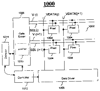
rows and columns. Since the OLED is a current driven device, the pixel circuit
of the
AMOLED should be capable of providing an accurate and constant drive current.
[0004] There is a need to provide a method and system that is capable of
providing constant
brightness with high accuracy.
SUMMARY OF THE INVENTION
[0005] It is an object of the invention to provide a method and system that
obviates or
mitigates at least one of the disadvantages of existing systems.
[0006] According to an aspect of the present invention there is provided a
display system
including one or more pixels. Each pixel includes a light emitting device, a
drive transistor
for driving the light emitting device, and a switch transistor for selecting
the pixel. The
display system includes a circuit for monitoring and extracting the change of
the pixel to
calibrate programming data for the pixel.
[0007] According to another aspect of the present invention there is provided
a method of
driving the display system. The display system includes one or more than
pixels. The
method includes the steps of at an extraction cycle, providing an operation
signal to the
pixel, monitoring a node in the pixel, extracting the aging of the pixel based
on the
-1-
CA 02576811 2007-02-09
monitoring result ; and at a programming cycle, calibrating programming data
based on the
extraction of the aging'of the pixel and providing the programming data to the
pixel.
BRIEF DESCRIPTION OF THE DRAWINGS
[0008] These and other features of the invention will become more apparent
from the
following description in which reference is made to the appended drawings
wherein:
Figure 1 illustrates an example of a pixel array having a 2-transistor (2T)
pixel circuit to
which a pixel operation technique in accordance with an embodiment of the
present
invention is suitably applied;
Figure 2 illustrates another example of a pixel array having a 2T pixel
circuit to which the
pixel operation technique associated with Figure 1 is suitably applied;
Figure 3A illustrates an example of signal waveforms applied to the pixel
circuits of Figures
1 and 2 during an extraction operation;
Figure 3B illustrates an example of signal waveforms applied to the pixel
circuits of Figures
I and 2 during a normal operation;
Figure 4 illustrates the effect of shift in the threshold voltage of a drive
transistor on the
voltage of VDD during the extraction cycles of Figure 3A;
Figure 5 illustrates an example of a display system having the pixel array of
Figure 1 or 2;
Figure 6 illustrates an example of normal and extraction cycles for driving
the pixel array of
Figure 5;
Figure 7 illustrates an example of a 3-transistor (3T) pixel circuit to which
a pixel operation
technique in accordance with another embodiment of the present invention is
suitably
applied;
Figure 8 illustrates another example of a 3T pixel circuit to which the pixel
operation
technique associated with Figure 7 is suitably applied;
-2-
CA 02576811 2007-02-09
Figure 9A illustrates an example of signal waveforms applied to the pixel
circuits of Figures
7 and 8 during an extraction operation;
Figure 9B illustrates an example of signal waveforms applied to the pixel
circuits of Figures
7 and 8 during a normal operation;
Figure 10 illustrates an example of a display system having the pixel circuit
of Figure 7 or
8;
Figure 11 A illustrates an example of normal and extraction cycles for driving
the pixel array
of Figure 10;
Figure 11 B illustrates another example of normal and extraction cycles for
driving the pixel
array of Figure 10;
Figure 12 illustrates another example of a display system having the pixel
circuit of Figure
7 or 8;
Figure 13 illustrates an example of normal and extraction cycles for driving
the pixel array
of Figure 12;
Figure 14 illustrates an example of a 4-transistor (4T) pixel circuit to which
a pixel operation
technique in accordance with a further embodiment of the present invention is
suitably
applied;
Figure 15 illustrates another example of a 4T pixel circuit to which the pixel
operation
technique associated with Figure 14 is suitably applied;
Figure 16A illustrates an example of signal wavefozms applied to the pixel
circuits of
Figures 14 and 15 during an extraction operation;
Figure 16B illustrates an example of signal waveforms applied to the pixel
circuits of
Figures 14 and 15 during a normal operation;
Figure 17 illustrates an example of a display system having the pixel circuit
of Figure 14 or
15;
-3-
CA 02576811 2007-02-09
Figure 18 illustrates an example of normal and extraction cycles for driving
the pixel array
of Figure 17;
Figure 19 illustrates another example of a display system having the pixel
circuit of Figure
14 or 15;
Figure 20 illustrates an example of normal and extraction cycles for driving
the pixel array
of Figure 19;
Figure 21 illustrates an example of a 3T pixel circuit to which a pixel
operation technique in
accordance with a further embodiment of the present invention is suitably
applied;
Figure 22 illustrates another example of a 3T pixel circuit to which the pixel
operation
technique associated with Figure 21 is suitably applied;
Figure 23A illustrates an example of signal waveforms applied to the pixel
circuits of
Figures 21 and 22 during an extraction operation;
Figure 23B illustrates an example of signal waveforms applied to the pixel
circuits of
Figures 21 and 22 during a normal operation;
Figure 24 illustrates an example of a display system having the pixel circuit
of Figure 21 or
22;
Figure 25A illustrates an example of normal and extraction cycles for driving
the pixel array
of Figure 24;
Figure 25B illustrates another example of normal and extraction cycles for
driving the pixel
array of Figure 24;
Figure 26 illustrates an example of a 3T pixel circuit to which a pixel
operation technique in
accordance with a further embodiment of the present invention is suitably
applied;
Figure 27 illustrates another example of a 3T pixel circuit to which the pixel
operation
technique associated with Figure 26 is suitably applied;
-4-
= CA 02576811 2007-02-09
Figure 28A illustrates an example of signal waveforms applied to the pixel
circuits of
Figures 26 and 27 during an extraction operation;
Figure 28B illustrates an example of signal waveforms applied to the pixel
circuits of
Figures 26 and 27 during a normal operation;
Figure 29 illustrates an example of a display system having the pixel circuit
of Figure 26 or
27;
Figure 30 illustrates an example of normal and extraction cycles for driving
the pixel array
of Figure 29;
Figure 31A illustrates a pixel circuit with readout capabilities at the jth
row and the ith
column;
Figure 31 B illustrates another pixel circuit with readout capabilities at the
jth row and the ith
column;
Figure 32 illustrates an example of a pixel circuit to which a driving
technique in accordance
with a further embodiment of the present invention is suitably applied;
Figure 33 illustrates an example of signal waveforms applied to the pixel
arrangement of
Figure 32;
Figure 34 illustrates another example of a pixel circuit to which the driving
technique
associated with Figure 32 is suitably applied;
Figure 35 illustrates an example of signal waveforms applied to the pixel
arrangement of
Figure 34;
Figure 36 illustrates an example of a pixel array in accordance with a further
embodiment of
the present invention;
Figure 37 illustrates RGBW structure using the pixel array of Figure 36; and
Figure 38 illustrates a layout for the pixel circuits of Figure 37.
-5-
CA 02576811 2007-02-09
DETAILED DESCRIPTION
[0009] Embodiments of the present invention are described using a pixel
circuit having a
light emitting device (e.g., an organic light emitting diode (OLED)), and a
plurality of
transistors. The transistors in the pixel circuit or in display systems in the
embodiments
below may be n-type transistors, p-type transistors or combinations thereof.
The transistors
in the pixel circuit or in the display systems in the embodiments below may be
fabricated
using amorphous silicon, nano/micro crystalline silicon, poly silicon, organic
semiconductors technologies (e.g. organic TFT), NMOS/PMOS technology or CMOS
technology (e.g. MOSFET). A display having the pixel circuit may be a single
color,
multi-color or a fully color display, and may include one or more than one
electroluminescence (EL) element (e.g., organic EL). The display may be an
active matrix
light emitting display (e.g., AMOLED). The display may be used in TVs, DVDs,
personal
digital assistants (PDAs), computer displays, cellular phones, or other
applications. The
display may be a flat panel.
[0010] In the description below, "pixel circuit" and "pixel" are used
interchangeably. In the
description below, "signal" and "line" may be used interchangeably. In the
description
below, the terms "line" and "node" may be used interchangeably. In the
description, the
terms "select line" and "address line" may be used interchangeably. In the
description
below, "connect (or connected)"and "couple (or coupled)" may be used
interchangeably,
and may be used to indicate that two or more elements are directly or
indirectly in physical
or electrical contact with each other. In the description, a pixel (circuit)
in the ith row and
the jth column may be referred to as a pixel (circuit) at position (i, j).
[0011 ] Figure 1 illustrates an example of a pixel array having a 2-transistor
(2T) pixel
circuit to which a pixel operation technique in accordance with an embodiment
of the
present invention is suitably applied. The pixel array 10 of Figure 1 includes
a plurality of
pixel circuits 12 arranged in "n" rows and "m" columns. In Figure 1, the pixel
circuits 12 in
the ith row are shown.
[0012] Each pixel circuit 12 includes an OLED 14, a storage capacitor 16, a
switch
transistor 18, and a drive transistor 20. The drain terminal of the drive
transistor 20 is
connected to a power supply line for the corresponding row (e.g., VDD(i)), and
the source
-6-
= CA 02576811 2007-02-09
terminal of the drive transistor 20 is connected to the OLED 14. One terminal
of the switch
transistor 18 is connected to a data line for the corresponding column (e.g.,
VDATA(1), ...
, or VDATA (m)), and the other terminal of the switch transistor 18 is
connected to the gate
terminal of the drive transistor 20. The gate terminal of the switch
transistor 18 is connected
to a select line for the corresponding row (e.g., SEL(i)). One terminal of the
storage
capacitor 16 is connected to the gate terminal of the drive transistor 20, and
the other
terminal of the storage capacitor 16 is connected to the OLED 14 and the
source terminal of
the drive transistor 20. The OLED 14 is connected between a power supply
(e.g., ground)
and the source terminal of the drive transistor 20. The aging of the pixel
circuit 12 is
extracted by monitoring the voltage of the power supply line VDD(i), as
described below.
[0013] Figure 2 illustrates another example of a pixel array having a 2T pixel
circuit to
which the pixel operation technique associated with Figure 1 is suitably
applied. The pixel
array 30 of Figure 2 is similar to the pixel array 10 of Figure 1. The pixel
circuit array 30
includes a plurality of pixel circuits 32 arranged in "n" rows and "m"
columns. In Figure
2, the pixel circuits 32 in the ith row are shown.
[0014] Each pixel circuit 32 includes an OLED 34, a storage capacitor 36, a
switch
transistor 38, and a drive transistor 40. The OLED 34 corresponds to the OLED
14 of Figure
1. The storage capacitor 36 corresponds to the storage capacitor 16 of Figure
1. The switch
transistor 38 corresponds to the switch transistor 18 of Figure 1. The drive
transistor 40
corresponds to the drive transistor 20 of Figure 1.
[0015] The source terminal of the drive transistor 40 is connected to a power
supply line for
the corresponding row (e.g., VSS(i)), and the drain terminal of the drive
transistor 40 is
connected to the OLED 34. One terminal of the switch transistor 38 is
connected to a data
line for the corresponding column (e.g., VDATA(1), ... , or VDATA (m)), and
the other
terminal of the switch transistor 38 is connected to the gate terminal of the
drive transistor
40. One terminal of the storage capacitor 34 is connected to the gate terminal
of the drive
transistor 40, and the other terminal of the storage capacitor 34 is connected
to the
corresponding power supply line (e.g., VSS(i)). The OLED 34 is connected
between a
power supply and the drain terminal of the drive transistor 40. The aging of
the pixel circuit
is extracted by monitoring the voltage of the power supply line VSS(i), as
described below.
-7-
= CA 02576811 2007-02-09
[0016] Figure 3A illustrates an example of signal waveforms applied to the
pixel circuits of
Figures 1 and 2 during an extraction operation. Figure 3B illustrates an
example of signal
waveforms applied to the pixel circuits of Figures 1 and 2 during a normal
operation. In
Figure 3A, VDD(i) is a power supply line/signal corresponding to VDD(i) of
Figure 1, and
VSS(i) is a power supply line/signal corresponding to VSS(i) of Figure 2. "Ic"
is a constant
current applied to VDD (i) of the pixel at position (i, j), which is being
calibrated. The
voltage generated on VDD (i) line as a result of the current Ic is (VcD+AVCD)
where VcD is
the DC biasing point of the circuit and AVcD is the amplified shift in the
OLED voltage and
threshold voltage of drive transistor (20 of Figure 1 or 40 of Figure 2).
[0017] Referring to Figures 1, 2 and 3A, the aging of the pixel at position
(i, j) is extracted
by monitoring the voltage of the power supply line (VDD (i) of Figure 1 or
VSS(i) of Figure
2). The operation of Figure 3A for the pixel at position (i, j) includes first
and second
extraction cycles 50 and 52. During the first extraction cycle 50, the gate
terminal of the
drive transistor (20 of Figure 1 or 40 of Figure 2) in the pixel at position
(i, j) is charged to
a calibration voltage VCG. This calibration voltage VCG includes the aging
prediction,
calculated based on the previous aging data, and a bias voltage. Also, the
other pixel circuits
in the ith row are programmed to zero during the first extraction cycle.
[0018] During the second extraction cycle 52, SEL(i) goes to zero and so the
gate voltage of
the drive transistor (20 of Figure 1 or 40 of Figure 2) in the pixel at
position (i, j) is affected
by the dynamic effects such as charge injection and clock feed-through. During
this cycle,
the drive transistor (20 of Figure 1 or 40 of Figure 2) acts as an amplifier
since it is biased
with a constant current through the power supply line for the ith row (VDD(i)
of Figure 1 or
VSS(i) of Figure 2). Therefore, the effects of shift in the threshold voltage
(VT) of the drive
transistor (20 of Figure 1 or 40 of Figure 2) in the pixel at position (i, j)
is amplified, and the
voltage of the power supply line (VDD(i) of Figure 1 or VSS(i) of Figure 2)
changes
accordingly. Therefore, this method enables extraction of very small amount of
VT shift
resulting in highly accurate calibration. The change in VDD (i) or VSS(i) is
monitored.
Then, the change(s) in VDD(i) or VSS(i) is used for calibration of programming
data.
[0019] Referring to Figures 1, 2 and Figure 3B, the normal operation for the
pixel at position
(i, j) includes a programming cycle 62 and a driving cycle 64. During the
programming
-8-
CA 02576811 2007-02-09
cycle 62, the gate terminal of the drive transistor (20 of Figure 1 or 40 of
Figure 2) in the
pixel at position (i, j) is charged to a calibrated programming voltage Vcp
using the
monitoring result (e.g., change(s) of VDD or VSS). This voltage Vcp is defined
by the gray
scale and the aging of the pixel (e.g., it is the sum of a voltage related to
a gray scale and the
aging extracted during the calibration cycles). Next, during the driving cycle
64, the select
line SEL(i) is low and the drive transistor (20 of Figure 1 or 40 of Figure 2)
in the pixel at
position (i, j) provides current to the OLED (14 of Figure 1 or 34 of Figure
2) in the pixel at
position (i, j).
[0020] Figure 4 illustrates the effect of shift in the threshold voltage of
the drive transistor.
(VT shift) on the voltage of the power supply line VDD during the extraction
cycles of
Figure 3A. It is apparent to one of ordinary skill in the art that the drive
transistor can
provide a reasonable gain so that makes the extraction of small VT shift
possible.
[0021 ] Figure 5 illustrates an example of a display system having the pixel
arrays of Figures
I and 2. The display system 1000 of Figure 5 includes a pixel array 1002
having a plurality
of pixels 1004. In Figure 5, four pixels 1004 are shown. However, the number
of the pixels
1004 may vary in dependence upon the system design, and does not limited to
four. The
pixel 1004 may be the pixel circuit 12 of Figure 1 or the pixel circuit 32 of
Figure 2. The
pixel array 1002 is an active matrix light emitting display, and may form an
AMOLED
display.
[0022] SEL(k) (k=i, i+l) is a select line for selecting the kth row, and
corresponds to SEL(i)
of Figures 1 and 2. V(k) is a power supply line and corresponds to VDD(j) of
Figure 1 and
VSS(j) of Figure 2. VDATA(l) (1=j, j+l ) is a data line and corresponds to one
of VDATA
(1), ..., VDATA(m) of Figures 1 and 2. SEL(k) and V(k) are shared between
common row
pixels in the pixel array 1002. VDATA(1) is shared between common column
pixels in the
pixel array 1002.
[0023] A gate driver 1006 drives SEL(k) and V(k). The gate driver 1006
includes an
address driver for providing address signals to SEL (k). The gate driver 1006
includes a
monitor 1010 for driving V(k) and monitoring the voltage of V(k). V(k) is
appropriately
activated for the operations of Figure 3A and 3B. A data driver 1008 generates
a
programming data and drives VDATA(1). Extractor block 1014 calculates the
aging of the
-9-
CA 02576811 2007-02-09
pixel based on the voltage generated on VDD(i). VDATA(1) is calibrated using
the
monitoring result (i.e., the change of the data line V(k)). The monitoring
result may be
provided to a controller 1012. The gate driver 1006, the controller 1012, the
extractor 1014,
or a combination thereof may include a memory for storing the monitoring
result. The
controller 1012 controls the drivers 1006 and 1008 and the extractor 1014 to
drive the pixels
1004 as described above. The voltages VCG, Vcp of Figure 3A and 3B are
generated using
the column driver.
[0024] Figure 6 illustrates an example of normal and extraction cycles for
driving the pixel
array 1002 of Figure 5. In Figure 6, each of ROWi (i=l, 2, ..) represents the
ith row; "P"
represents a programming cycle and corresponds to 60 of Figure 3B; "D"
represents a
driving cycle and corresponds to 62 of Figure 3B; "E1" represents a first
extraction cycle
and corresponds to 50 of Figure 3A; and "E2" represents a second extraction
cycle and
corresponds to 52 of Figure 3A. The extraction can happen at the end of each
frame during
the blanking time. During this time, the aging of several pixels can be
extracted. Also, an
extra frame can be inserted between several frames in which all pixels are
OFF. During this
frame, one can extract the aging of several pixels without affecting the image
quality.
[0025] Figure 7 illustrates an example of a 3-transistor (3T) pixel circuit to
which a pixel
operation technique in accordance with another embodiment of the present
invention is
suitably applied. The pixel circuit 70 of Figure 7 includes an OLED 72, a
storage capacitor
74, a switch transistor 76, and a drive transistor 78. The pixel circuit 70
forms an AMOLED
display.
[0026] The drain terminal of the drive transistor 78 is connected to a power
supply line
VDD, and the source terminal of the drive transistor 78 is connected to the
OLED 72. One
terminal of the switch transistor 76 is connected to a data line VDATA, and
the other
terminal of the switch transistor 76 is connected to the gate terminal of the
drive transistor
78. The gate terminal of the switch transistor 76 is connected to a first
select line SEL I.
One terminal of the storage capacitor 74 is connected to the gate terminal of
the drive
transistor 78, and the other terminal of the storage capacitor 74 is connected
to the OLED 72
and the source terminal of the drive transistor 78.
-10-
CA 02576811 2007-02-09
[0027] A sensing transistor 80 is provided to the pixel circuit 70. The
transistor 80 may be
included in the pixel circuit 70. One terminal of the transistor 80 is
connected to an output
line VOUT, and the other terminal of the transistor 80 is connected to the
source terminal of
the drive transistor 78 and the OLED 72. The gate terminal of the transistor
80 is connected
to a second select line SEL2.
[0028] The aging of the pixel circuit 70 is extracted by monitoring the
voltage of the output
line VOUT. In one example, VOUT may be provided separately from VDATA. In
another
example, VOUT may be a data line VDATA for a physically adjacent column (row).
SELl
is used for programming, while SEL1 and SEL2 are used for extracting pixel
aging.
[0029] Figure 8 illustrates another example of a 3T pixel circuit to which the
pixel operation
technique associated with Figure 7 is suitably applied. The pixel circuit 90
of Figure 8
includes an OLED 92, a storage capacitor 94, a switch transistor 96, and a
drive transistor
98. The OLED 92 corresponds to the OLED 72 of Figure 7. The storage capacitor
94
corresponds to the storage capacitor 74 of Figure 7. The transistors 96 and 98
correspond to
the transistors 76 and 78 of Figure 7. The pixel circuit 90 forms an AMOLED
display.
[0030] The source terminal of the drive transistor 98 is connected to a power
supply line
VSS, and the drain terminal of the drive transistor 98 is connected to the
OLED 92. The
switch transistor 96 is connected between a data line VDATA and the gate
terminal of the
drive transistor 98. The gate terminal of the switch transistor 96 is
connected to a first select
line SEL 1. One terminal of the storage capacitor 94 is connected to the gate
terminal of the
drive transistor 98, and the other terminal of the storage capacitor 94 is
connected to VSS.
[0031 ] A sensing transistor 100 is provided to the pixel circuit 90. The
transistor 100 may
be included in the pixel circuit 90. One terminal of the transistor 100 is
connected to an
output line VOUT, and the other terminal of the transistor 100 is connected to
the drain
terminal of the drive transistor 98 and the OLED 92. The gate terminal of the
transistor 100
is connected to a second select line SEL2.
[0032] The aging of the pixel circuit 90 is extracted by monitoring the
voltage of the output
line VOUT. In one example, VOUT may be provided separately from VDATA. In
another
-11-
CA 02576811 2007-02-09
example, VOUT may be a data line VDATA for a physically adjacent column (row).
SEL1
is used for programming, while SEL1 and SEL2 are used for extracting pixel
aging.
[0033] Figure 9A illustrates an example of signal waveforms applied to the
pixel circuits of
Figures 7 and 8 during an extraction operation. Figure 9B illustrates an
example of signal
waveforms applied to the pixel circuits of Figures 7 and 8 during a normal
operation.
[0034] Referring to 7, 8 and Figures 9A, the extraction operation for the
pixel at position (i,
j) includes first and second extraction cycles 110 and 112. During the first
extraction cycle
110, the gate terminal of the drive transistor (78 of Figure 7 or 98 of Figure
8) is charged to
a calibration voltage VCG. This calibration voltage VcG includes the aging
prediction,
calculated based on the previous aging data. During the second extraction
cycle 112, the
first select line SEL1 goes to zero, and so the gate voltage of the drive
transistor (78 of
Figure 7 or 98 of Figure 8) is affected by the dynamic effects including the
charge injection
and clock feed-through. During the second extraction cycle 112, the drive
transistor (78 of
Figure 7 or 98 of Figure 8) acts as an amplifier since it is biased with a
constant current (Ic)
through VOUT. The voltage developed on VOUT as a result of current Ic applied
to it is
(VCb+OVCD). Therefore, the aging of the pixel is amplified, and the voltage of
the VOUT
changes accordingly. Therefore, this method enables extraction of very small
amount of
voltage threshold (VT) shift resulting in highly accurate calibration. The
change in VOUT
is monitored. Then, the change(s) in VOUT is used for calibration of
programming data.
[0035] Also, applying a current/voltage to the OLED during the extraction
cycle, the
voltage/current of the OLED can be extracted, and the system determines the
aging factor of
the OLED and uses it for more accurate calibration of the luminance data.
[0036] Referring to 7, 8 and 9B, the normal operation for the pixel at
position (i, j) includes
a programming cycle 120 and a driving cycle 122. During the programming cycle
120, the
gate terminal of the drive transistor (78 of Figure 7 or 98 of Figure 8) is
charged to a
calibrated programming voltage VcP using the monitoring result (e.g., the
changes of
VOUT). Next, during the driving cycle 122, the select line SEL1 is low and the
drive
transistor (78 of Figure 7 or 98 of Figure 8) provides current to the OLED (72
of Figure 7,
or 92 of Figure 8).
-12-
CA 02576811 2007-02-09
[0037] Figure 10 illustrates an example of a display system having the pixel
circuit of Figure
7 or 8. The display system 1020 of Figure 10 includes a pixel array 1022
having a plurality
of pixels 1004 arranged in row and column. In Figure 10, four pixels 1024 are
shown.
However, the number of the pixels 1024 may vary in dependence upon the system
design,
and does not limited to four. The pixel 1024 may be the pixel circuit 70 of
Figure 7 or the
pixel circuit 90 of Figure 8. The pixel array 1022 is an active matrix light
emitting display,
and may be an AMOLED display.
[0038] SEL 1(k) (k=i, i+l ) is a first select line for selecting the kth row,
and corresponds to
SEL1 of Figures 7 and 8. SEL2(k) (k=i, i+l ) is a second select line for
selecting the kth row,
and corresponds to SEL2 of Figures 7 and 8. VOUT(1) (1 j, j+l ) is an output
line for the lth
column, and corresponds to VOUT of Figures 7 and 8. VDATA(l) is a data line
for the Ith
column, and corresponds to VDATA of Figures 7 and 8.
[0039] A gate driver 1026 drives SEL 1(k) and SEL2(k). The gate driver 1026
includes an
address driver for providing address signals to SELl(k) and SEL2(k). A data
driver 1028
generates a programming data and drives VDATA(1). The data driver 1028
includes a
monitor 1030 for driving and monitoring the voltage of VOUT(1). Extractor
block 1034
calculates the aging of the pixel based on the voltage generated on VOUT(i).
VDATA(1) and
VOUT (1) are appropriately activated for the operations of Figure 9A and 9B.
VDATA(I) is
calibrated using the monitoring result (i.e., the change of VOUT(l)). The
monitoring result
may be provided to a controller 1032. The data driver 1028, the controller
1032, the
extractor 1034, or a combination thereof may include a memory for storing the
monitoring
result. The controller 1032 controls the drivers 1026 and 1028 and the
extractor 1034 to
drive the pixels 1004 as described above.
[0040] Figure I 1 A and 11 B illustrate two examples of normal and extraction
cycles for
driving the pixel array of Figure 10. In Figure 11A and 11B, each of ROWi
(i=1, 2, ..)
represents the ith row; "P" represents a programming cycle and corresponds to
120 of Figure
9B; "D" represents a driving cycle and corresponds to 122 of Figure 9B; "E1"
represents a
first extraction cycle and corresponds to 110 of Figure 9A; and "E2"
represents a second
extraction cycle and corresponds to 112 of Figure 9A. In Figure 11 A, the
extraction can
happen at the end of each frame during the blanking time. During this time,
the aging of
-13-
CA 02576811 2007-02-09
several pixels can be extracted. Also, an extra frame can be inserted between
several frames
in which all pixels are OFF. During this frame, one can extract the aging of
several pixels
without affecting the image quality. Figure 11 B shows a case in which one can
do the
extraction in parallel with programming cycle.
[0041 ] Figure 12 illustrates another example of a display system having the
pixel circuit of
Figure 7 or 8. The display system 1040 of Figure 12 includes a pixel array
1042 having a
plurality of pixels 1044 arranged in row and column. The display system 1040
is similar to
the display system 1020 of Figure 10. In Figure 12, data line VDATA (j+l) is
used as an
output line VOUT(}) for monitoring the ageing of pixel.
[0042] A gate driver 1046 is the same or similar to the gate driver 1026 of
Figure 10. The
gate driver 1046 includes an address driver for providing address signals to
SEL1(k) and
SEL2(k). A data driver 1048 generates a programming data and drives VDATA(1).
The
data driver 1048 includes a monitor 1050 for monitoring the voltage of
VDATA(1).
VDATA(1) is appropriately activated for the operations of Figure 9A and 9B.
Extractor
block 1054 calculates the aging of the pixel based on the voltage generated on
VDATA.
VDATA(1) is calibrated using the monitoring result (i.e., the change of
VDATA(l)). The
monitoring result may be provided to a controller 1052. The data driver 1048,
the controller
1052, the extractor 1054, or a combination thereof may include a memory for
storing the
monitoring result. The controller 1052 controls the drivers 1046 and 1048 and
the extractor
1054 to drive the pixels 1004 as described above.
[0043] Figure 13 illustrates an example of normal and extraction cycles for
driving the
pixel array 1042 of Figure 12. In Figure 13, each of ROWi (i=1, 2, ..)
represents the ith row;
"P" represents a programming cycle and corresponds to 120 of Figure 9B; "D"
represents a
driving cycle and corresponds to 122 of Figure 9B; "E 1" represents a first
extraction cycle
and corresponds to 110 of Figure 9A; and "E2" represents a second extraction
cycle and
corresponds to 112 of Figure 9A. The extraction can happen at the end of each
frame during
the blanking time. During this time, the aging of several pixels can be
extracted. Also, an
extra frame can be inserted between several frames in which all pixels are
OFF. During this
frame, one can extract the aging of several pixels without affecting the image
quality.
-14-
CA 02576811 2007-02-09
[0044] Figure 14 illustrates an example of a 4-transistor (4T) pixel circuit
to which a pixel
operation technique in accordance with a further embodiment of the present
invention is
suitably applied. The pixel circuit 130 of Figure 14 includes an OLED 132, a
storage
capacitor 134, a switch transistor 136, and a drive transistor 138; The pixel
circuit 130
forms an AMOLED display.
[0045] The drain terminal of the drive transistor 138 is connected to the OLED
132, and the
source terminal of the drive transistor 138 is connected to a power supply
line VSS (e.g.,
ground). One terminal of the switch transistor 136 is connected to a data line
VDATA, and
the other terminal of the switch transistor 136 is connected to the gate
terminal of the drive
transistor 138. The gate terminal of the switch transistor 136 is connected to
a select line
SEL[j]. One terminal of the storage capacitor 134 is connected to the gate
terminal of the
drive transistor 138, and the other terminal of the storage capacitor 134 is
connected to VSS.
[0046] A sensing network 140 is provided to the pixel circuit 130. The network
140 may be
included in the pixel circuit 130. The circuit 140 includes transistors 142
and 144. The
transistors 142 and 144 are connected in series between the drain terminal of
the drive
transistor 138 and an output line VOUT. The gate terminal of the transistor
142 is connected
to a select line SEL[j+1 ]. The gate terminal of the transistor 144 is
connected to a select line
SEL[j-1].
[0047] The select line SEL[k] (k j-1, j, j+l) may be an address line for the
kth row of a pixel
array. The select line SEL[j-1] or SEL[j+l] may be replaced with SEL[j] where
SEL[j] is
ON when both of SEL[j-1] and SEL[j+1] signals are ON.
[0048] The aging of the pixel circuit 130 is extracted by monitoring the
voltage of the output
line VOUT. In one example, VOUT may be provided separately from VDATA. In
another
example, VOUT may be a data line VDATA for a physically adjacent column (row).
[0049] Figure 15 illustrates another example of a 4T pixel circuit to which
the pixel
operation technique associated with Figure 14 is suitably applied. The pixel
circuit 150 of
Figure 15 includes an OLED 152, a storage capacitor 154, a switch transistor
156, and a
drive transistor 158. The pixel circuit 150 forms an AMOLED display. The OLED
152
-15-
CA 02576811 2007-02-09
corresponds to the OLED 132 of Figure 14. The storage capacitor 154
corresponds to the
storage capacitor 134 of Figure 14. The transistors 156 and 158 correspond to
the transistors
136 and 138 of Figure 14.
[0050] The source terminal of the drive transistor 158 is connected to the
OLED 152, and
the drain terminal of the drive transistor 158 is connected to a power supply
line VDD. The
switch transistor 156 is connected between a data line VDATA and the gate
terminal of the
drive transistor 158. One terminal of the storage capacitor 154 is connected
to the gate
terminal of the drive transistor 158, and the other terminal of the storage
capacitor 154 is
connected to the OLED 152 and the source terminal of the drive transistor 158.
[0051 ] A sensing network 160 is provided to the pixel circuit 150. The
network 160 may be
included in the pixel circuit 150. The circuit 160 includes transistors 162
and 164. The
transistors 162 and 164 are connected in series between the source terminal of
the drive
transistor 158 and an output line VOUT. The gate terminal of the transistor
162 is connected
to a select line SEL(j-1 ]. The gate terminal of the transistor 164 is
connected to a select line
SEL[j+l]. The transistors 162 and 164 correspond to the transistors 142 and
144 of Figure
14.
[0052] The aging of the pixel circuit 150 is extracted by monitoring the
voltage of the output
line VOUT. In one example, VOUT may be provided separately from VDATA. In
another
example, VOUT may be a data line VDATA for a physically adjacent column (row).
[0053] Figure 16A illustrates an example of signal waveforms applied to the
pixel circuits
of Figures 14 and 15 during an extraction operation. Figure 16B illustrates an
example of
signal waveforms applied to the pixel circuits of Figures 14 and 15 during a
normal
operation.
[0054] Referring to 14, 15 and Figures 16A, the extraction operation for the
pixel at position
(i, j) includes first and second extraction cycles 170 and 172. During the
first extraction
cycle 170, the gate terminal of the drive transistor (138 of Figure 14 or 158
of Figure 15) is
charged to a calibration voltage VCG. This calibration voltage VCG includes
the aging
prediction, calculated based on the previous aging data. During the second
extraction cycle
172, the select line SEL[i] goes to zero, and so the gate voltage of the drive
transistor (138
-16-
CA 02576811 2007-02-09
of Figure 14 or 158 of Figure 15) is affected by the dynamic effects including
the charge
injection and clock feed-through. During the second extraction cycle 172, the
drive
transistor (138 of Figure 14 or 158 of Figure 15) acts as an amplifier since
it is biased with
a constant current through VOUT. The voltage developed on VOUT as a result of
current
Ic applied to it is (VcD+AVCD). Therefore, the aging of the pixel is
amplified, and change the
voltage of the VOUT. Therefore, this method enables extraction of very small
amount of
voltage threshold (VT) shift resulting in highly accurate calibration. The
change in VOUT is
monitored. Then, the change(s) in VOUT is used for calibration of programming
data.
[0055] Also, applying a current/voltage to the OLED during the extraction
cycle, the sytem
can extract the voltage/current of the OLED and determines the aging factor of
the OLED
and use it for more accurate calibration of the luminance data.
[0056] Referring to 14, 15 and 16B, the normal operation for the pixel at
position (i, j)
includes a programming cycle 180 and a driving cycle 182. During the
programming cycle
180, the gate terminal of the drive transistor (138 of Figure 14 or 158 of
Figure 15) is
charged to a calibrated programming voltage Vcp using the monitoring result
(e.g., the
changes of VOUT). During the driving cycle 182, the select line SEL[i] is low
and the drive
transistor (13 8 of Figure 14 or 158 of Figure 15) provides current to the
OLED (142 of
Figure 14 or 152 of Figure 15).
[0057] Figure 17 illustrates an example of a display system having the pixel
circuit of Figure
14 or 15 where VOUT is separated from VDATA. The display system 1060 of Figure
17 is
similar to the display system 1020 of Figure 10. The display system 1060
includes a pixel
array having a plurality of pixels 1064 arranged in row and column. In Figure
17, four pixels
1064 are shown. However, the number of the pixels 1064 may vary in dependence
upon the
system design, and does not limited to four. The pixel 1064 may be the pixel
circuit 130 of
Figure 14 or the pixel circuit 150 of Figure 15. The pixel array of Figure 13
is an active
matrix light emitting display, and may be an AMOLED display.
[0058] SELI(k) (k=i-1, i, i+1, i+2) is a select line for selecting the kth
row, and corresponds
to SEL[j-1], SEL[j] and SEL[j+1] of Figures 14 and 15. VOUT(1) (1 j, j+1) is
an output line
for the lth column, and corresponds to VOUT of Figures 14 and 15. VDATA(1) is
a data line
for the lth column, and corresponds to VDATA of Figures 14 and 15.
-17-
CA 02576811 2007-02-09
[0059] A gate driver 1066 drives SEL(k). The gate driver 1066 includes an
address driver
for providing address signals to SEL(k). A data driver 1068 generates a
programming data
and drives VDATA(l). The data driver 1068 includes a monitor 1070 for driving
and
monitoring the voltage of VOUT(l). Extractor block 1074 calculates the aging
of the pixel
based on the voltage generated on VOUT(1). VDATA(1) and VOUT (1) are
appropriately
activated for the operations of Figure 16A and 16B. VDATA(1) is calibrated
using the
monitoring result (i.e., the change of VOUT(l)). The monitoring result may be
provided to
a controller 1072. The data driver 1068, the controller 1072, the extractor
1074, or a
combination thereof may include a memory for storing the monitoring result.
The controller
1072 controls the drivers 1066 and 1068 and the extractor 1074 to drive the
pixels 1064 as
described above.
[0060] Figure 18 illustrates an example of the normal and extraction cycles
for driving the
pixel array of Figure 17. In Figure 18, each of ROWi (i=1, 2, ..) represents
the ith row; "P"
represents a programming cycle and corresponds to 180 of Figure 16B; "D"
represents a
driving cycle and corresponds to 182 of Figure 16B; "El" represents the first
and second
extraction cycle and corresponds to 170 of Figure 16A; and "E2" represents a
second
extraction cycle and corresponds to 172 of Figure 16A. The extraction can
happen at the end
of each frame during the blanking time. During this time, the aging of several
pixels can be
extracted. Also, an extra frame can be inserted between several frames in
which all pixels
are OFF. During this frame, one can extract the aging of several pixels
without affecting the
image quality.
[0061] Figure 19 illustrates another example of a display system having the
pixel circuit of
Figure 14 or 15 where VDATA is used as VOUT. The display system 1080 of Figure
19 is
similar to the display system 1040 of Figure 12. The display system 1080
includes a pixel
array having a plurality of pixels 1084 arranged in row and column. In Figure
19, four pixels
1084 are shown. However, the number of the pixels 1084 may vary in dependence
upon the
system design, and does not limited to four. The pixel 1084 may be the pixel
circuit 130 of
Figure 14 or the pixel circuit 150 of Figure 15. The pixel array of Figure 19
is an active
matrix light emitting display, and may be an AMOLED display.
-18-
CA 02576811 2007-02-09
[0062] In the display system of Figure 19, VDATA is used as a data line for
the lth column
and an output line for monitoring the pixel aging.
[0063] A gate driver 1066 drives SEL(k). The gate driver 1086 includes an
address driver
for providing address signals to SEL(k). A data driver 1088 generates a
programming data
and drives VDATA(1). The data driver 1088 includes a monitor 1090 for driving
and
monitoring the voltage of VDATA(1). Extractor block 1094 calculates the aging
of the pixel
based on the voltage generated on VDATA(1). VDATA(1) is appropriately
activated for the
operations of Figure 16A and 16B. VDATA(1) is calibrated using the monitoring
result (i.e.,
the change of VDATA(1)). The monitoring result may be provided to a controller
1092. The
data driver 1088, the controller 1092, the extractor 1094, or a combination
thereof may
include a memory for storing the monitoring result. The controller 1092
controls the drivers
1086 and 1088 and the extractor 1094 to drive the pixels 1084 as described
above.
[0064] Figure 20 illustrates an example of the normal and extraction cycles
for driving the
pixel array of Figure 19. In Figure 20, each of ROWi (i=1, 2, ..) represents
the ith row; "P"
represents a programming cycle and corresponds to 180 of Figure 16B; "D"
represents a
driving cycle and corresponds to 182 of Figure 16B; "El" represents the first
extraction
cycle and corresponds to 170 of Figure 16A; and "E2" represents a second
extraction cycle
and corresponds to 172 of Figure 16A. The extraction can happen at the end of
each frame
during the blanking time. During this time, the aging of several pixels can be
extracted.
Also, an extra frame can be inserted between several frames in which all
pixels are OFF.
During this frame, one can extract the aging of several pixels without
affecting the image
quality.
[0065] Figure 21 illustrates an example of a 3T pixel circuit to which a pixel
operation
scheme in accordance with a further embodiment of the present invention is
suitably
applied. The pixel circuit 190 of Figure 21 includes an OLED 172, a storage
capacitor 194,
a switch transistor 196, and a drive transistor 198. The pixel circuit 190
forms an AMOLED
display.
[0066] The drain terminal of the drive transistor 198 is connected to the OLED
192, and the
source terminal of the drive transistor 198 is connected to a power supply
line VSS (e.g.,
ground). One terminal of the switch transistor 196 is connected to a data line
VDATA, and
-19-
CA 02576811 2007-02-09
the other terminal of the switch transistor 196 is connected to the gate
terminal of the drive
transistor 198. The gate terminal of the switch transistor 196 is connected to
a select line
SEL. One terminal of the storage capacitor 194 is connected to the gate
terminal of the drive
transistor 198, and the other terminal of the storage capacitor 194 is
connected to VSS.
[0067] A sensing transistor 200 is provided to the pixel circuit 190. The
transistor 200 may
be included in the pixel circuit 190. The transistor 200 is connected between
the drain
terminal of the drive transistor 198 and an output line VOUT. The gate
terminal of the
transistor 200 is connected to the select line SEL.
[0068] The aging of the pixel circuit 190 is extracted by monitoring the
voltage of the output
line VOUT. SEL is shared by the switch transistor 196 and the transistor 200.
[0069] Figure 22 illustrates another example of a 3-transistor (3T) pixel
circuit to which the
pixel operation technique associated with Figure 21 is suitably applied. The
pixel circuit
210 of Figure 22 includes an OLED 212, a storage capacitor 214, a switch
transistor 216,
and a drive transistor 218. The OLED 212 corresponds to the OLED 192 of Figure
21. The
storage capacitor 214 corresponds to the storage capacitor 194 of Figure 21.
The transistors
216 and 218 correspond to the transistors 196 and 198 of Figure 21. The pixel
circuit 210
forms an AMOLED display.
[0070] The drain terminal of the drive transistor 218 is connected to a power
supply line
VDD, and the source terminal of the drive transistor 218 is connected to the
OLED 212. The
switch transistor 216 is connected between a data line VDATA and the gate
terminal of the
drive transistor 218. One terminal of the storage capacitor 214 is connected
to the gate
terminal of the drive transistor 218, and the other terminal of the storage
capacitor 214 is
connected to the source terminal of the drive transistor 218 and the OLED 212.
[0071 ] A sensing transistor 220 is provided to the pixel circuit 210. The
transistor 220 may
be included in the pixel circuit 210. The transistor 220 connects the source
terminal of the
drive transistor 218 and the OLED 212 to an output line VOUT. The transistor
220
corresponds to the transistor 200 of Figure 21. The gate terminal of the
transistor 220 is
connected to the select line SEL.
-20-
CA 02576811 2007-02-09
[0072] The aging of the pixel circuit 210 is extracted by monitoring the
voltage of the output
line VOUT. SEL is shared by the switch transistor 216 and the transistor 220.
[0073] Figure 23A illustrates an example of signal waveforms applied to the
pixel circuits
of Figures 21 and 22 during an extraction operation. Figure 23B illustrates an
example of
signal waveforms applied to the pixel circuits of Figures 21 and 22 during a
normal
operation.
[0074] Referring to 21, 22 and Figures 23A, the extraction operation includes
an extraction
cycle 170. During the extraction cycle 170, the gate terminal of the drive
transistor (198 of
Figure 21 or 218 of Figure 22) is charged to a calibration voltage VcG. This
calibration
voltage VcG includes the aging prediction, calculated based on the previous
aging data.
During the extraction cycle 230, the drive transistor (198 of Figure 21 or 218
of Figure 22)
acts as an amplifier since it is biased with a constant current through VOUT.
The voltage
developed on VOUT as a result of current Ic applied to it is (VCD+OVCD).
Therefore, the
aging of the pixel is amplified, and change the voltage of the VOUT.
Therefore, this method
enables extraction of very small amount of voltage threshold (VT) shift
resulting in highly
accurate calibration. The change in VOUT is monitored. Then, the change(s) in
VOUT is
used for calibration of programming data
[0075] Afso, applying a current/voltage to the OLED during extraction cycle,
the system can
extract the voltage/current of the OLED and determines the aging factor of the
OLED and
use it for more accurate calibration of the luminance data.
[0076] Referring to 21, 22 and 23B, the normal operation includes a
programming cycle 240
and a driving cycle 242. During the programming cycle 240, the gate terminal
of the drive
transistor (198 of Figure 21 or 218 of Figure 22) is charged to a calibrated
programming
voltage Vcp using the monitoring result (i.e., the changes of VOUT). During
the driving
cycle 242, the select line SEL is low and the drive transistor (198 of Figure
21 or 218 of
Figure 22) provides current to the OLED (192 of Figure 21 or 212 of Figure
22).
[0077] Figure 24 illustrates an example of a display system having the pixel
circuit of Figure
21 or 22 where VOUT is separated from VDATA. The display system 1100 of Figure
24
includes a pixel array having a plurality of pixels 1104 arranged in row and
column. In
-21-
CA 02576811 2007-02-09
Figure 24, four pixels 1104 are shown. However, the number of the pixels 1104
may vary
in dependence upon the system design, and does not limited to four. The pixel
1104 may be
the pixel circuit 190 of Figure 21 or the pixel circuit 210 of Figure 22. The
pixel array of
Figure 24 is an active matrix light emitting display, and may be an AMOLED
display.
[0078] SEL(k) (k=i, i+1) is a select line for selecting the kth row, and
corresponds to SEL
of Figures 21 and 22. VOUT(1) (1 j, j+1) is an output line for the lth column,
and
corresponds to VOUT of Figures 21 and 22. VDATA(1) is a data line for the lth
column, and
corresponds to VDATA of Figures 21 and 22.
[0079] A gate driver 1106 drives SEL(k). The gate driver 1106 includes an
address driver
for providing address signals to SEL(k). A data driver 1108 generates a
programming data
and drives VDATA(l). The data driver 1108 includes a monitor 1110 for driving
and
monitoring the voltage of VOUT(1). Extractor block 1114 calculates the aging
of the pixel
based on the voltage generated on VOUT(1). VDATA(1) and VOUT (1) are
appropriately
activated for the operations of Figure 23A and 23B. VDATA(l) is calibrated
using the
monitoring result (i.e., the change of VOUT(1)). The monitoring result may be
provided to
a controller 1112. The data driver 1108, the controller 1112, the extractor
1114, or a
combination thereof may include a memory for storing the monitoring result.
The controller
1112 controls the drivers 1106 and 1108 and the extractor 1114 to drive the
pixels 1104 as
described above.
[0080] Figures 25A and 25B illustrate two examples of the normal and
extraction cycles for
driving the pixel array of Figure 24. In Figure 25A and 25B, each of ROWi
(i=1, 2, ..)
represents the ith row; "P" represents a programming cycle and corresponds to
240 of Figure
23B; "D" represents a driving cycle and corresponds to 242 of Figure 23B; "E1"
represents
the first extraction cycle and corresponds to 230 of Figure 23A. In Figure
25A, the
extraction can happen at the end of each frame during the blanking time.
During this time,
the aging of several pixels can be extracted. Also, an extra frame can be
inserted between
several frames in which all pixels are OFF. During this frame, one can extract
the aging of
several pixels without affecting the image quality. In Figure 25B, the
extraction and
programming happens in parallel.
-22-
CA 02576811 2007-02-09
[0081] Figure 26 illustrates an example of a 3T pixel circuit to which a pixel
operation
technique in accordance with a further embodiment of the present invention is
suitably
applied. The pixel circuit 260 of Figure 26 includes an OLED 262, a storage
capacitor 264,
a switch transistor 266, and a drive transistor 268. The pixel circuit 260
forms an AMOLED
display.
[0082] The OLED 262 corresponds to the OLED 192 of Figure 21. The capacitor
264
corresponds to the capacitor 194 of Figure 21. The transistors 264 and 268
correspond to the
transistors 196 and 198 of Figure 21, respectively. The gate terminal of the
switch transistor
266 is connected to a first select line SEL I.
[0083] A sensing transistor 270 is provided to the pixel circuit 260. The
transistor 270 may
be included in the pixel circuit 260. The transistor 270 is connected between
the drain
terminal of the drive transistor 268 and VDATA. The gate terminal of the
transistor 270 is
connected to a second select line SEL2.
[0084] The aging of the pixel circuit 260 is extracted by monitoring the
voltage of VDADA.
VDATA is shared for programming and extracting the pixel aging.
[0085] Figure 27 illustrates another example of a 3T pixel circuit to which
the pixel
operation technique associated with Figure 26 is suitably applied. The pixel
circuit 280 of
Figure 27 includes an OLED 282, a storage capacitor 284, a switch transistor
286, and a
drive transistor 288. The pixel circuit 280 forms an AMOLED display.
[0086] The OLED 282 corresponds to the OLED 212 of Figure 22. The capacitor
284
corresponds to the capacitor 214 of Figure 22. The transistors 284 and 288
correspond to the
transistors 216 and 218 of Figure 22, respectively. The gate terminal of the
switch transistor
286 is connected to a first select line SEL1.
[0087] A sensing transistor 290 is provided to the pixel circuit 280. The
transistor 290 may
be included in the pixel circuit 280. The transistor 290 is connected between
the source
terminal of the drive transistor 288 and VDATA. The transistor 290 corresponds
to the
transistor 270 of Figure 26. The gate terminal of the transistor 290 is
connected to a second
select line SEL2.
-23-
CA 02576811 2007-02-09
[0088] The aging of the pixel circuit 280 is extracted by monitoring the
voltage of VDADA.
VDATA is shared for programming and extracting the pixel aging.
[0089] Figure 28A illustrates an example of signal waveforms applied to the
pixel circuits
of Figures 26 and 27 during an extraction operation. Figure 28B illustrates an
example of
signal waveforms applied to the pixel circuits of Figures 26 and 27 during a
normal
operation.
[0090] Referring to 26, 27 and Figures 28A, the extraction operation includes
first and
second extraction cycles 300 and 302. During the first extraction cycle 300,
the gate
terminal of the drive transistor (268 of Figure 26 or 288 of Figure 27) is
charged to a
calibration voltage V. This calibration voltage VCG includes the aging
prediction,
calculated based on the previous aging data. During the second extraction
cycle 302, the
drive transistor (268 of Figure 26 or 288 of Figure 27) acts as an amplifier
since it is biased
with a constant current through VDATA. Therefore, the aging of the pixel is
amplified, and
the voltage of the VDATA changes accordingly. Therefore, this method enables
extraction
of very small amount of voltage threshold (VT) shift resulting in highly
accurate calibration.
The change in VDATA is monitored. Then, the change(s) in VDATA is used for
calibration of programming data
[0091 ] Also, applying a current/voltage to the OLED during extraction cycle,
the system can
extract the voltage/current of the OLED and determines the aging factor of the
OLED and
use it for more accurate calibration of the luminance data.
[0092] Referring to 26, 27 and 28B, the normal operation includes a
programming cycle 310
and a driving cycle 312. During the programming cycle 310, the gate terminal
of the drive
transistor (268 of Figure 26 or 288 of Figure 27) is charged to a calibrated
programming
voltage VcP using the monitoring result (i.e., the changes of VDATA). Next,
during the
driving cycle 312, the select line SEL1 is low and the drive transistor (268
of Figure 26 or
288 of Figure 27) provides current to the OLED (262 of Figure 26, or 282 of
Figure 27).
[0093] Figure 29 illustrates an example of a display system having the pixel
circuit of Figure
26 or 27. The display system 1120 of Figure 29 includes a pixel array having a
plurality of
pixels 1124 arranged in row and column. In Figure 29, four pixels 1124 are
shown.
-24-
CA 02576811 2007-02-09
However, the number of the pixels 1124 may vary in dependence upon the system
design,
and does not limited to four. The pixel 1024 may be the pixel circuit 260 of
Figure 26 or the
pixel circuit 280 of Figure 27. The pixel array of Figure 29 is an active
matrix light emitting
display, and may be an AMOLED display.
[0094] SEL 1(k) (k=i, i+l ) is a first select line for selecting the kth row,
and corresponds to
SEL1 of Figures 26 and 27. SEL2(k) (k=i, i+1) is a second select line for
selecting the kth
row, and corresponds to SEL2 of Figures 26 and 27. VDATA(1) (1 j, j+1) is a
data line for
the lth column, and corresponds to VDATA of Figures 26 and 27.
[0095] A gate driver 1126 drives SEL 1(k) and SEL2(k). The gate driver 1126
includes an
address driver for providing address signals to SEL1(k) and SEL2(k). A data
driver 1128
generates a programming data and drives VDATA(l). The data driver 1128
includes a
monitor 1130 for driving and monitoring the voltage of VDATA(1). Extractor
block 1134
calculates the aging of the pixel based on the voltage generated on VDATA(i).
VDATA(1)
is appropriately activated for the operations of Figure 28A and 28B. VDATA(1)
is calibrated
using the monitoring result (i.e., the change of VDATA(1)). The monitoring
result may be
provided to a controller 1132. The data driver 1128, the controller 1132, the
extractor 1134
or a combination thereof may include a memory for storing the monitoring
result. The
controller 1132 controls the drivers 1126 and 1128 and the extractor 1134 to
drive the pixels
1124 as described above.
[0096] Figure 30 illustrates an example of normal and extraction cycles for
driving the pixel
array of Figure 29. In Figure 30, each of ROWi (i=l, 2,..) represents the ith
row; "P"
represents a programming cycle and corresponds to 310 of Figure 28B; "D"
represents a
driving cycle and corresponds to 312 of Figure 28B; "El" represents the first
extraction
cycle and corresponds to 300 of Figure 28A; "E2" represents the second
extraction cycle and
corresponds to 302 of Figure 28A. the extraction can happen at the end of each
frame during
the blanking time. During this time, the aging of several pixels can be
extracted. Also, an
extra frame can be inserted between several frames in which all pixels are
OFF. During this
frame, one can extract the aging of several pixels without affecting the image
quality.
[0097] According to the embodiments of the present invention illustrated in
Figures 1 to
28B, pixel aging is extracted, and the pixel programming or biasing data is
calibrated, which
-25-
CA 02576811 2007-02-09
provides a highly accurate operation. According to the embodiments of the
present
invention, the programming/biasing of a flat panel becomes highly accurate
resulting in less
error. Thus it facilitates the realization of high-resolution large-are flat
panels for displays
and sensors.
[0098] Programming and reading out technique using shared data lines and
select lines is
fiirther described in detail using Figure 31A to 35.
[0099] Figures 31 A and 31 B illustrate pixel circuits with readout
capabilities at the jth row
and the ith column. The pixel of Figure 31A includes a driver circuit 352 for
driving a light
emitting device (e.g., OLED), and a sensing circuit 356 for monitoring an
acquisition data
from the pixel. A transistor 354 is provided to connect a data line DATA[i] to
the driver
circuit 352 based on a signal on a select line SEL[j]. A transistor 358 is
provided to connect
the output from the monitoring circuit 356 to a readout line Readout[i]. In
Figure 31A, the
pixel is programmed through the data line DATA[i] via the transistor 354, and
the
acquisition data is read back through the readout line Readout[i] via the
transistor 358.
[00100] The sensing circuit 356 may be a sensor, TFT, or OLED itself. The
system
of Figure 31A uses an extra line (i.e., Readout [i]).
[00101] In the pixel of Figure 31B the transistor 358 is connected to the data
line
DATA[i] or an adjacent data line, e.g., DATA[i-l], DATA[i+l]. The transistor
354 is
selected by a first select line SEL1 [i] while the transistor 358 is selected
by an extra select
line SEL2[i]. In Figure 31B, the pixel is programmed through the data line
DATA[i] via the
transistor 354, and the acquisition data is read back through the same data
line or a data line
for an adjacent row via the transistor 358. Although, the number of rows in a
panel is
generally less than the number of columns, the system of Figure 31 B uses the
extra select
lines.
[00102] Figure 32 illustrates an example of a pixel circuit to which a pixel
operation
technique in accordance with a further embodiment of the present invention is
suitably
applied. The pixel circuit 370 of Figure 32 is at the jth row and ith column.
In Figure 32, the
data and readout line are merged without adding extra select line. The pixel
circuit 370 of
Figure 32 includes a driver circuit 372 for driving a light emitting device
(e.g. OLED), and
-26-
CA 02576811 2007-02-09
a sensing circuit 376 for sensing an acquisition data from the pixel. A
transistor 374 is
provided to connect a data line DATA[i] to the driver circuit 372 based on a
signal on a
select line SEL[i]. The pixel is programmed while SEL[j] is high. A sensing
network 378
is provided to the sensing circuit 376.
[00103] The sensing circuit 376 senses the pixel electrical, optical, or
temperature
signals of the driver circuit 352. Thus, the output of the sensing circuit 376
determines the
pixel aging overtime. The monitor circuit 376 may be a sensor, a TFT, a TFT of
the pixel,
or OLED of the pixel (e.g., 14 of Figure 1).
[00104] In one example, the sensing circuit 376 is connected, via the sensing
network
378, to the data line DATA[i] of the column in which the pixel is. In another
example, the
sensing circuit 376 is connected, via the sensing network 378, a data line for
one of the
adjacent columns e.g., DATA [i+l], or DATA[i-l]..
[00105] The sensing network 378 includes transistors 380 and 382. The
transistors
380 and 382 are connected in series between the output of the monitor circuit
376 and a data
line, e.g., DATA[i], DATA[i-1], DATA[i+l]. The transistor 380 is selected by a
select line
for an adjacent row, e.g., SEL[i-1], SEL[i+t]. The transistor 382 is selected
by the select
line SEL[i], which is also connected to the gate terminal of the transistor
374.
[00106] The driver circuit 372, the monitor circuit 376, and the switches 374,
380 and
382 may be fabricated in amorphous silicon, poly silicon, organic
semiconductor, or CMOS
technologies.
[00107] The arrangement of Figure 32 can be used with different timing
schedule.
However, one of them is shown in Figure 33. The operation cycles of Figure 33
includes a
programming cycle 380, a driving cycle 392, and a readback cycle 394.
[00108] Referring to Figures 32 and 33, during the programming cycle 390, the
pixel
is programmed through DATA[i] while SEL[i] is ON During the driving cycle 392,
SEL[i]
goes OFF. For the readout process 394, SEL[i] and one adjacent row's select
line SEL[i-1 ]
or SEL[j+l ] are ON, and so the monitoring data is read back through DATA[i],
DATA[i-1 ]
or DATA[i+l] which is connected to the sensing network 378.
-27-
CA 02576811 2007-02-09
[00109] The transistors 380 and 382 can be easily swapped without affecting
the
readout process.
[00110] Figure 34 illustrates another example of a pixel circuit to which the
pixel
operation technique associated with Figure 32 is suitably applied. The pixel
circuit 400 of
Figure 34 is at the jth row and ith column. In Figure 34, the data and readout
line are merged
without adding extra select line. The pixel circuit 400 of Figure 34 includes
an OLED (now
shown), the driver circuit 372, and the sensing circuit 376. A sensing network
408 is
provided to the sensing circuit 376. The sensing network 408 includes
transistors 410 and
412. The transistor 410 and 412 are same or similar to the transistors 380 and
382 of Figure
32, respectively. The gate terminal of the transistor 410 is connected to a
select line
SEL[j-1] for the (j-1)th row. The gate terminal of the transistor 412 is
connected to a select
line SEL[j+1 ] for the (j+1)th row. The pixel is programmed while SEL[i] is
high. The
transistor 412 may be shared by more than one pixel.
[00111] In one example, the monitoring circuit 3 76 is connected, via the
sensing
network 408, to the data line DATA[j] of the column in which the pixel is. In
another
example, the monitoring circuit 376 is connected, via the sensing network 408,
a data line
for one of the adjacent columns e.g., DATA [i+1 ], DATA[i-1 ].
[00112] The switches 410 and 412 can be fabricated in amorphous silicon, poly
silicon, organic semiconductor, or CMOS technologies.
[00113] The arrangement of Figure 34 can be used with different timing
schedule.
However, one of them is shown in Figure 35. The operation cycles of Figure 35
includes a
programming cycle 420, a driving cycle 422, and a readback cycle 424.
[00114] Referring to Figures 34 and 35, during the programming cycle 420, the
pixel
is programmed through DATA[i] while SEL[j] is ON During the driving cycle 422,
SEL[j]
goes Off. For the readout process 424, SEL[j-1] and are ON, and so the
monitoring data is
read back through DATA[i], DATA[i-1] or DATA[i+l] which is connected to the
sensing
network 408. The transistors 410 and 412 can be easily exchanged without
affecting the
readout process.
-28-
õ . ' CA 02576811 2007-02-09
[00115] The display systems having the pixel structures of Figures 31 and 34
are
similar to those of the display system described above. Data read back from
the sensing
network is used to calibrate programming data.
[00116] The technique according to the embodiments of the present invention
illustrated in Figures 32 to 40 shares the data line used to program the pixel
circuit and the
readout line used to extract the pixel aging data without affecting the pixie
circuit operation
and without adding extra controlling signal. The number of signals connected
to the panel
is reduced significantly. Thus the complexity of the driver is reduced. It
reduces the
implementation cost of the external driver decreases and reduces the cost of
calibration
tourniquets in active matrix light emitting displays, in particular AMOLED
displays.
[00117] A technique for increasing the aperture ratio pixel circuits of the
calibration
techniques is described in detail using Figures 36 to 38.
[00118] Figure 36 illustrates an example of a pixel array in accordance with a
further
embodiment of the present invention. The pixel array 500 of Figure 36 includes
a plurality
of pixel circuits 510 arranged in rows and columns. In Figure 36, two pixels
510 in the jth
column are shown. The pixel circuit 510 includes an OLED 512, a storage
capacitor 514, a
switch transistor 516, and a drive transistor 518. The OLED 512 corresponds to
the OLED
212 of Figure 22. The storage capacitor 514 corresponds to the storage
capacitor 214 of
Figure 22. The transistors 516 and 518 correspond to the transistors 216 and
218 of Figure
22.
[00119] The drain terminal of the drive transistor 518 is connected to a power
supply
line VDD, and the source terminal of the drive transistor 518 is connected to
the OLED 512.
The switch transistor 516 is connected between a corresponding data line Data
[j] and the
gate terminal of the drive transistor 518. One terminal of the storage
capacitor 514 is
connected to the gate terminal of the drive transistor 518, and the other
terminai of the
storage capacitor 514 is connected to the source terminal of the drive
transistor 518 and the
OLED 512.
[00120] A sensing network 550 is provided to the pixel array 500. The network
550
includes a sensing transistor 532 for each pixel and a sensing transistor 534.
The transistor
-29-
CA 02576811 2007-02-09
532 may be included in the pixel 500. The sensing transistor 534 is connected
to a plurality
of switch transistors 532 for a plurality of pixels 510. In Figure 36, the
sensing transistor
534 is connected to two switch transistors 532 for two pixels 510 in the jth
column.
[00121] The transistor 532 for the pixel 510 at position (i, j) is connected
to a data line
DATA 0+1] via the transistor 534, and is also connected to the OLED 512 in the
pixel 510
at position (i, j). Similarly, the transistor 532 for the pixel 510 at
position (i-h, j) is
connected to the data line DATA 0+1] via the transistor 534, and is also
connected to the
OLED 512 in the pixel 510 at position (i-h,j). DATA 0+1] is a data line for
programming
the (j+1) th column.
[00122] The transistor 532 for the pixel 510 at position (i, j) is selected by
a select line
SEL[k] for the "k"th row. The transistor 532 for the pixel 510 at position (i-
h, j) is selected
by a select line SEL[k'] for the k' th row. The sensing transistor 534 is
selected by a select
line SEL[t] for the "t"th row. There can be no relation among "i", "i-h", "k",
"k"", and "t".
However, to have a compact pixel circuit for a higher resolution, it is better
that they be
consecutive. The two transistors 532 are connected to the transistor 534
through an internal
line, i.e., monitor line [j, j+1].
[00123] The pixels 510 in one column are divided into few segments (each
segments
has 'h' number of pixels). In the pixel array 500 of 36, the two pixels in one
column are in
one segment. A calibration component (e.g., transistor 534) is shared by the
two pixels.
[00124] In Figure 36, the pixel at the jth column is programmed through the
data line,
DATA[j], and the acquisition data is read back through the data line for an
adjacent column,
e.g., DATA [j+l] (or DATA [j-1]). Since SEL(i) is OFF during programming and
during
extraction, the switch transistor 516 is OFF. The sensing switch 534 grantees
a conflict free
readout and programming procedures.
[00125] Figure 37 illustrates RGBW structure using the pixel array 500 of
Figure 36.
In Figure 37, two pixels form one segment. In Figure 37, "CSR", "T1R", "T2R",
and
"T3R" are components for a pixel for red "R", and correspond to 514, 518, 516,
and 532 of
Figure 36; "CSG", "T1 G", "T2G", and "T3G" are components for a pixel for
green "G", and
correspond to 514, 518, 516, and 532 of Figure 36; "CSB", "TIB", "T2B", and
"T3B" are
-30-
CA 02576811 2007-02-09
components for a pixel for blue "B", and correspond to 514, 518, 516, and 532
of Figure 36;
"CSW", "T1 W", "T2W", and "T3W" are components for a pixel for white "W", and
correspond to 514, 518, 516, and 532 of Figure 36.
[00126] In Figure 37, "TWB" represents a sensing transistor shared by two
pixels for
"W" and "B", and corresponds to the sensing transistor 534 of Figure 36; and
"TGR"
represents a sensing transistor shared by two pixels for "G" and "R", and
corresponds to the
sensing transistor 534 of Figure 36.
[00127] The gate terminals of the transistors T3W and T3G are connected to a
select
line SEL[i] for the ith row. The gate terminals of the transistors T3B and T3R
are connected
to a select line SEL[i+l ] for the ith row. The gate terminal of the sensing
transistor TWB and
the gate terminal of the sensing transistor TGR are connected to the select
line SEL[i] for the
ith row.
[00128] The sensing transistors TWB and TGR of the two adjacent segments which
use the SEL[i] for sensing is put in the segment area of pixels which use SEL
[i] for
programming to reduce the layout complexity where one segment includes two
pixel which
shares the same sensing transistor.
[00129] Figure 38 illustrates a layout for the pixel circuits of Figure 37. In
Figure 45,
"R" is an area associated with a pixel for read; "G" is an area associated
with a pixel for
green; "B" is an area associated with a pixel for blue; "W" is an area
associated with a pixel
for white. "TWB" corresponds to the sensing transistor TWB of Figure 37, and
shared by
the pixel for while and the pixel for while. "TGR" corresponds to the sensing
transistors
TGR of Figure 37, and is shared by the pixel for green and the pixel for red.
The size of the
pixel is, for example, 208um x 208 um. It shows the applicability of the
circuit to a very
small pixel for high resolution displays
[00130] One or more currently preferred embodiments have been described by way
of example. It will be apparent to persons skilled in the art that a number of
variations and
modifications can be made without departing from the scope of the invention as
defined in
the claims.
-31-