Note : Les descriptions sont présentées dans la langue officielle dans laquelle elles ont été soumises.
CA 02577395 2012-07-10
1
CONFIGURABLE RECURSIVE DIGITAL FILTER FOR PROCESSING
TELEVISION AUDIO SIGNALS
FIELD OF THE INVENTION
[0002] This disclosure relates to processing television audio signals and,
more
particularly, to a configurable architecture for use with encoding and
decoding television
audio signals.
BACKGROUND OF THE INVENTION
[0003] In 1984, the United States, under the auspices of the Federal
Communications
Commission, adopted a standard for the transmission and reception of stereo
audio for
television. This standard is codified in the FCC's Bulletin OET-60, and is
often called the
BTSC system after the Broadcast Television Systems Committee that proposed it,
or the
MTS (Multi-channel Television Sound) system.
[004] Prior to the BTSC system, broadcast television audio was monophonic,
consisting of a single "channel" or signal of audio content. Stereo audio
typically
requires the transmission of two independent audio channels, and receivers
capable
of detecting and recovering both channels. In order to meet the FCC's
requirement that
the new transmission standard be 'compatible' with existing monophonic
television
sets (i.e., that mono receivers be capable of reproducing an appropriate audio
signal
from the new type of stereo broadcast), the Broadcast Television Systems
Committee
adopted an approach similar to FM radio systems: stereo Left and Right audio
signals
are combined to form two new signals, a Sum signal and a Difference signal.
[005] Monophonic television receivers detect and demodulate only the Sum
signal,
CA 02577395 2012-07-10
2
consisting of the addition of the Left and Right stereo signals. Stereo-
capable receivers
receive both the Sum and the Difference signals, recombining the signals to
extract the
original stereo Left and Right signals.
[0006] For transmission, the Sum signal directly modulates the aural FM
carrier just as
would a monophonic audio signal. The Difference channel, however, is first
modulated
onto an AM subcarrier located 31.768 kHz above the aural carrier's center
frequency. The
nature of FM modulation is such that background noise increases by 3 decibel
(dB) per
octave, and as a result, because the new subcarrier is located further from
the aural
carrier's center frequency than the Sum or mono signal, additional noise is
introduced into
the Difference channel, and hence into the recovered stereo signal. In many
circumstances,
in fact, this rising noise characteristic renders the stereo signal too noisy
to meet the
requirements imposed by the FCC, and so the BTSC system mandates a noise
reduction
system in the Difference channel signal path.
[0007] This system, sometimes referred to as dbx noise reduction (after the
company
that developed the technique) is of the companding type, comprising an encoder
and
decoder. The encoder adaptively filters the Difference signal prior to
transmission such
that amplitude and frequency content, upon decoding, hide ("mask") noise
picked up
during the transmission process. The decoder completes the process by
restoring the
Difference signal to original form and thereby ensuring that noise is audibly
masked by the
signal content.
[0008] The dbx noise reduction system is also used to encode and decode
Secondary
Audio Programming (SAP) signals, which is defined in the BTSC standard as an
additional information channel and is often used to e.g., carry programming in
an
alternative language, reading services for the blind, or other services.
[0009] Cost is, of course, of prime concern to television manufacturers. As a
result of
intense competition and consumer expectations, profit margins on consumer
electronics
products, especially television products, can be vanishingly small. Because
the dbx
CA 02577395 2012-07-10
=
3
decoder is located in the television receiver, manufacturers are sensitive to
the cost of the
decoder, and reducing the cost of the decoder is a necessary and worthwhile
goal. While
the encoder is not located in a television receiver and is not as sensitive
from a profit
standpoint, any development which will decrease manufacturing costs of the
encoder also
provides a benefit.
SUMMARY OF THE INVENTION
[0010] In accordance with an aspect of the disclosure, a television audio
signal
encoder includes a device that sums a left channel audio signal and a right
channel audio
signal to produce a sum signal. The matrix also subtracts one of the left and
right audio
signals from the other to produce a difference signal. The encoder also
includes a
configurable infinite impulse response digital filter that selectively uses
one or more sets
of filter coefficients to filter the difference signal. The set of filter
coefficients is applied to
the difference signal by a single multiplier in a recursive manner to prepare
the difference
signal for transmission.
[0011] In one embodiment, the configurable infinite impulse response digital
filter
may include a feedback path to apply the set of filter coefficients to the
difference signal in
a recursive manner. This feedback path may include a shift register to delay
digital signals
associated with the difference signal. The configurable infinite impulse
response digital
filter may multiple a signal associated with the difference signal and provide
an output of
this multiplication. The configurable infinite impulse response clignat titter
may include a
selector that selects a digital input signal or selects one of the filter
coefficients. In some
arrangements the selector may include a multiplexer. The infinite impulse
response digital
filter may be configured to provide various filtering functions such as a low
pass filter.
The configurable infinite impulse response digital filter may also include a
single adder for
applying the filter coefficients to the difference signal in a recursive
manner. The
television audio signal may comply to the Broadcast Television System
Committee (BTSC)
standard, the Near Instantaneously Companded Audio Muliplex (N1CAM) standard,
the
A2/Zweiton standard, the EIA. ¨ J standard, or other similar audio standard.
The
CA 02577395 2012-07-10
4
configurable infinite impulse response digital filter may be implemented in an
integrated
circuit.
[0012] In accordance with another aspect of the disclosure, a television audio
signal
decoder includes a configurable infinite impulse response digital filter that
selectively uses
one or more sets of filter coefficients to filter a difference signal. The
difference signal is
produced by subtracting one of a left channel and a right channel audio signal
from the
other audio signal. The set of filter coefficients is applied to the
difference signal by a
single multiplier in a recursive manner to prepare the difference signal for
separating the
left channel and right channel audio signals. The decoder also includes a
device that
separates the left channel and right channel audio signals from the difference
signal and a
sum signal. The sum signal includes the sum the left channel audio signal and
the right
channel audio signal.
[0013] In one embodiment, the configurable infinite impulse response digital
filter
may include a feedback path to apply the set of filter coefficients to the
difference signal in
a recursive manner. This feedback path may include a shift register to delay
digital signals
associated with the difference signal. The configurable infinite impulse
response digital
filter may multiple a signal associated with the difference signal and provide
an output of
this multiplication. The configurable infinite impulse response digital filter
may include a
selector that selects a digital input signal or selects one of the filter
coefficients. In some
arrangements the selector may include a multiplexer. The infinite impulse
response digital
filter may be configured to provide various filtering functions such as a low
pass filter.
The configurable infinite impulse response digital filter may also include a
single adder for
applying the filter coefficients to the difference signal in a recursive
manner. The
television audio signal may comply to the Broadcast Television System
Committee (BTSC)
standard, the Near Instantaneously Companded Audio Muliplex (NICAM) standard,
the
A2/Zweiton standard, the EIA ¨ J standard, or other similar audio standard.
The
configurable infinite impulse response digital filter may be implemented in an
integrated
circuit.
CA 02577395 2013-02-28
As an aspect of the present invention, there is provided a television audio
signal
decoder, comprising: a separation device configured to run at a clock speed
and to
separate the left channel and right channel audio signals from the difference
signal and
a sum signal, wherein the sum signal includes the sum of the left channel
audio signal
and the right channel audio signal; and a configurable infinite impulse
response (IIR)
digital filter configured to run at a selected clock speed substantially
faster than the
clock speed of the separation device and to selectively use, over a sampling
period, at
least one set of filter coefficients multiple times to filter a difference
signal, wherein the
difference signal is produced by subtracting one of a left channel and a right
channel
audio signal from the other of the left channel and right channel audio
signal, wherein
the at least one set of filter coefficients is applied to the difference
signal by a single
multiplier in a recursive manner in a recursive loop to prepare the difference
signal for
separating the left channel and right channel audio signals, wherein the
configurable
II R digital filter includes a feedback path and is configured to apply the at
least one set
of filter coefficients to the difference signal in a recursive manner, and
wherein the
configurable IIR digital filter is operable to change the at least one set of
filter
coefficients between iterations of the recursive loop.
As another aspect of the present invention, there is provided a television
audio
signal encoder for processing a left channel audio signal and a right channel
audio
signal and including signal paths requiring a plurality of filters for use at
various stages
of signal processing, the encoder comprising an arrangement configured to sum
a left
channel audio signal and a right channel audio signal to produce a sum signal,
and to
subtract one of the left and right audio signals from the other of the left
and right signals
to produce a difference signal, wherein the encoder comprises: at least one
infinite
impulse response digital filter, wherein the infinite impulse response digital
filter is
reconfigurable during processing of the left channel audio signal and the
right channel
audio signal, and includes a first signal selector for selectively receiving
input signals
to at least two of the filters for separately processing each of the input
signals in
accordance with a respective filtering operation, and a second signal selector
for
receiving signals representing sets of filter coefficients each corresponding
to one of the
respective one of the filter operations; wherein the selectors are used to
select at any
one time the input signal and the corresponding set of filter coefficients
applied to the
CA 02577395 2013-02-28
5a
input signal in a recursive manner by the infinite impulse response digital
filter so that
the infinite impulse response digital filter can selectively perform each of
the filtering
operations of at least two of the filters during processing of the left
channel audio signal
and the right channel audio signal.
As another aspect of the present invention, there is provided a television
audio
signal decoder for processing a television audio signal encoded with a sum
signal and
a difference signal representing a left channel audio signal and a right
channel audio
signal and including signal paths requiring a plurality of filters for use at
various stages
of signal processing, the decoder including an arrangement configured to
separate the
left channel audio signal and the right channel audio signal, wherein the
decoder
comprises: at least one infinite impulse response digital filter, wherein the
infinite
impulse response digital filter is reconfigurable during processing of the sum
signal and
the difference signal, and includes a first signal selector for selectively
receiving input
signals to at least two of the filters for separately processing each of the
input signals
in accordance with a respective filtering operation, and a second signal
selector for
receiving signals representing sets of filter coefficients each corresponding
to one of the
respective one of the filter operations; wherein the selectors are used to
select at any
one time the input signal and the corresponding set of filter coefficients
applied to the
input signal in a recursive manner by the infinite impulse response digital
filter so that
the infinite impulse response digital filter can selectively perform each of
the operations
of at least two of the filters during processing of the sum signal and the
difference
signal.
[0014] Additional advantages and aspects of the present disclosure will become
readily apparent to those skilled in the art from the following detailed
description,
wherein embodiments of the present invention are shown and described, simply
by way
of illustration of the best mode contemplated for practicing the present
invention. As will
be described, the present disclosure is capable of other and different
embodiments,
and its several details are susceptible of modification in various obvious
respects.
Accordingly, the drawings and description are to be regarded as illustrative
in nature,
and not as !imitative.
CA 02577395 2013-02-28
5b
BRIEF DESCRIPTION OF THE DRAWINGS
FIG. 1 is a block diagram representing a television signal transmission system
that is configured to comply with the BTSC television audio signal standard.
FIG. 2 is a block diagram representing a portion of a BTSC encoder included in
the television signal transmission system shown in FIG. 1.
FIG. 3 is a block diagram representing a television receiver system that is
configured to receive and decode BTSC television audio signals sent by the
television
signal transmission system shown in FIG. 1.
FIG. 4 is a block diagram representing a portion of a BTSC decoder included in
the television receiver system shown in FIG. 3.
FIG. 5 is a diagrammatic view of a configurable infinite impulse response
filter
for performing operations of the encoder and decoder shown in FIG. 2 and FIG.
4.
FIG. 6 is a graphical representation of a transfer function of a second-order
infinite impulse response filter that may be implemented by the infinite
impulse
response filter shown in FIG. 5.
FIG. 7 is a block diagram of a portion of a BTSC encoder that highlights
operations that may be performed by the configurable infinite impulse response
filter
shown in FIG.5.
CA 02577395 2012-07-10
6
FIG. 8 is a block diagram of a portion of a BTSC decoder that highlights
operations
that may be performed by the configurable infinite impulse response filter
shown in FIG.
5.
DETAILED DESCRIPTION OF THE PREFERRED EMBODIMENTS
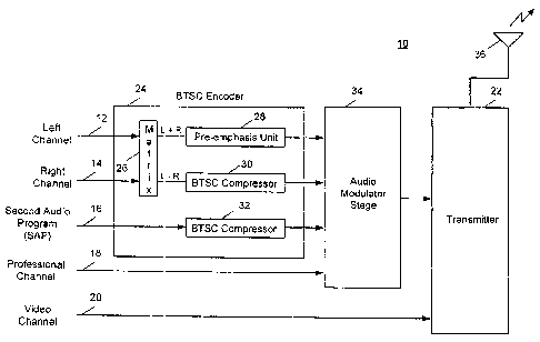
[0015] Referring to FIG 1, a functional block diagram of a BTSC compatible
television signal transmitter 10 includes five lines (e.g., conductive wires,
cables, etc.) that
provide signals for transmission. In particular, left and right audio channels
are provided
on respective lines 12 and 14. An SAP signal is provided by line 16 in which
the signal has
content to provide additional channel information (e.g., alternative
languages, etc.). A
fourth line 18 provides a professional channel that is typically used by
broadcast television
and cable television companies. Video signals are provided by a line 20 to a
transmitter 22.
=
The left, right, and SAP channels are provided to a BTSC encoder 24 that
prepares the
audio signals for transmission. Specifically, the left and right audio
channels are provided
to a matrix 26 that calculates a sum signal (e.g., L + R) and a difference
signal (e.g., L¨ R)
from the audio signals. Typically operations of matrix 26 are performed by
utilizing a
digital signal processor (DSP) or similar hardware or software ¨ based
techniques known
to one skilled in the art of television audio and video signal processing.
Once produced,
sum and difference signals (i.e., L + R and L ¨ R) are encoded for
transmission. In
particular, the sum signal (i.e., L + R) is provided to a pre-emphasis unit 28
that alters the
magnitude of select frequency components of the sum signal with respect to
other
frequency components. The alteration may be in a negative sense in which the
magnitude
of the select frequency components are suppressed, or the alteration may be in
a positive
sense in which the magnitude of the select frequency components are enhanced.
[0016] The difference signal (i.e., L ¨ R) is provided to a BTSC compressor 30
that
adaptively filters the signal prior to transmission such that when decoded,
the signal
amplitude and frequency content suppress noise imposed during transmission_
Similar to
the difference signal, the SAP signal is provided to a BTSC compressor 32. An
audio
CA 02577395 2012-07-10
õ
modulator stage 34 receives the processed sum signal, difference signal, and
SAP signal.
Additionally, signals from,the professional channel are provided to audio
modulator stage
34. The four signals are modulated by audio modulator stage 34 and provided to
transmitter 22. Along with the video signals provided by the video channel,
the four audio
signals are conditioned for transmission and provided to an antenna 36 (or an
antenna
system). Various signal transmitting techniques known to one skilled in the
art of
television systems and telecommunications may be implemented by transmitter 22
and
antenna 36. For example, transmitter 22 may be incorporated into a cable
television
system, a broadcast television system, or other similar television system.
[0017] Referring to FIG 2, a block diagram representing operations performed
by a
portion of BTSC compressor 30 is shown. In general, the difference channel
(i.e., L ¨ R)
processing performed by BTSC compressor 30 is considerably mOre complex than
the
sum channel (i.e., L + R) processing by pre-emphasis unit 28. The additional
processing
provided by the difference channel processing BTSC compressor 30, in
combination with
complementary processing provided by a decoder (not shown) receiving a BTSC
signal,
maintains the signal-to-noise ratio of the difference channel at acceptable
levels even in
the presence of the higher noise floor associated with the transmission and
reception of the
difference channel. BTSC compressor 30 essentially generates the encoded
difference
signal by dynamically compressing, or reducing the dynamic range of the
difference signal
so that the encoded signal may be transmitted through a limited dynamic range
iTA minks-inn rath and so that a decoder receiving the encoded signal may
recover
substantially all the dynamic range in the original difference signal by
expanding the
compressed difference signal in a complementary fashion. In some arrangements,
BTSC
compressor 30 implements a particular form of an adaptive signal weighing
system
described in U.S. Patent No. 4,539,526, and which is known to be advantageous
for
transmitting a signal having a relatively large dynamic range through a
transmission path
having a relatively narrow, frequency dependent, dynamic range.
CA 02577395 2012-07-10
8
[0018] The BTSC standard rigorously defines the desired operation of BTSC
encoder
24 and BTSC compressors 30 and 32. Specifically, the BTSC standard provides
transfer
functions and/or guidelines for the operation of each component included e.g.,
in BTSC
compressor 30 and the transfer functions are described in terms of
mathematical
representations of idealized analog filters. Upon receiving the difference
signal (i.e., L¨R)
from matrix 26, the signal may be provided to an interpolation and fixed pre-
emphasis
stage 38. In some digital BTSC encoders, the interpolation is set for twice
the sample rate
and the interpolation may be accomplished by linear interpolation, parabolic
interpolation,
or a filter (e.g., a finite impulse response (FIR) filter, an infinite impulse
response (UR)
filter, etc.) of n-th order. The interpolation and fixed pre-emphasis stage 38
also provides
pre-emphasis. After interpolation and pre-emphasis, the difference signal is
provided to a
divider 40 that divides the difference signal by a quantity determined from
the difference
signal and described in detail below.
[0019] The output of divider '40'n is provided to a spectral compression unit
42 that
performs emphasis filtering of the difference signal. In general, spectral
compression unit
42 "compresses", or reduces the dynamic range, of the difference signal by
amplifying
signals having relatively low amplitudes and attenuating signals having
relatively large
amplitudes. In some arrangements spectral compression unit 42 produces an
internal
control signal from the difference signal that controls the pre-emphasis/de-
emphasis that is
applied. Typically, spectral compression unit 42 dynamically compresses high
frequency
portions of the difference signal by an amount determined by the energy level
in the high
frequency portions of the encoded difference signal. Spectral compression unit
42 thus
provides additional signal compression toward the higher frequency portions of
the
difference signal. This is done because the difference signal tends to be
noisier in the
higher frequency portion of the spectrum_ When the encoded difference signal
is decoded
with a spectral expander in a decoder, respectively in a complementary manner
to the
spectral compression unit of the encoder, the signal ¨ to ¨ noise ratio of the
L ¨ R signal is
substantially preserved.
CA 02577395 2012-07-10
_
9
[0020] Once processed by spectral compression unit 42, the difference signal
is
provided to an over-modulation protection unit 44 and band-limiting unit 46.
Similar to
the other components, the BTSC standard provides suggested guidelines for the
operation
of over-modulation protection unit 44 and band-limiting unit 46. Generally,
band-limiting
unit 46 and a portion of over-modulation protection unit 44 may be implemented
as low
pass filters. Over-modulation protection unit 44 also performs as a threshold
device that
limits the amplitude of the encoded difference signal to full modulation,
where full
modulation is the maximum permissible deviation level for modulating an audio
subcarrier in a television signal.
[0021] Two feedback paths 48 and 50 are included in BTSC compressor 30.
Feedback
path 50 includes a spectral control bandpass filter 52 that typically has a
relatively narrow
pass band that is weighted towards higher audio frequencies to provide a
control signal for
spectral compression unit 42. To condition the control signal produced by
spectral control
bandpass filter 52, feedbick,path 50 also includes a multiplier 54 (configured
to square the.
signal provided by spectral control bandpass filter 52), an integrator 56, and
a square root
device that provides the control signal to spectral compression unit 42.
Feedback path 48
also includes a bandpass filter (i.e., gain control bandpass filter 60) that
filters the output
signal from band-limiting unit 46 to set the gain applied to the output signal
of
interpolation and fixed pre-emphasis stage 38 via divider 40. Similar to
feedback path 50,
feedback path 48 also includes a multiplier 62, an integrator 64, and a square
root device
66 Lu euntliiiun the sigrial that ia provided to dividf-r= 40.
[0022] Referring to FIG 3, a block diagram is shown that represents a
television
receiver system 68 that includes an antenna 70 (or a system of antennas) to
receive BTSC
compatible broadcast signals from television transmission system 10 (shown in
FIG 1).
The signals received by antenna 70 are provided to a receiver 72 that is
capable of
detecting and isolating the television transmission signals. However, in some
arrangements receiver 72 may receive the BTSC compatible signals from another
television signal transmission technique known to one skilled in the art of
television signal
CA 02577395 2012-07-10
,
=
.10
broadcasting. For example, the television signals may be provided to receiver
72 over a
cable television system or a satellite television network.
[0023] Upon receiving the television signals, receiver 72 conditions (e.g.,
amplifies,
filters, frequency scales, etc.) the signals and separates the video signals
and the audio
signals out of the transmission signals. The video content is provided to a
video
processing system 74 that prepares the video content contained in the video
signals for
presentation on a screen (e.g., a cathode ray tube, etc.) associated with the
television
receiver system 68. Signals containing the separate audio content are provided
to a
demodulator stage 76 that e.g., removes the modulation applied to the audio
signals at
television transmission system 10. The demodulated audio signals (e.g., the
SAP channel,
the professional channel, the sum signal, the difference signal) are provided
to a BTSC
decoder 78 that appropriately decodes each signal. The SAP channel is provided
a SAP
channel decoder 80 and the professional channel is provided to a professional
channel
deCodef '82. After separating the SAP channel and the professional, .channel,
a
demodulated sum signal (i.e., L + R signal) is provided to a de-emphasis unit
84 that
processes the sum signal in a substantially complementary fashion in
comparison to
pre-emphasis unit 28 (shown in FIG 1). Upon de-emphasizing the spectral
content of the
sum signal, the signal is provided to a matrix 88 for separating the left and
right channel
audio signals.
[0024] The difference signal (i.e., L ¨ R) is also demodulated by demodulation
stage
76 and is provided to a BTSC expander 86 included in BTSC decoder 78. BTSC
expander
86 complies with the BTSC standard, and as described in detail below,
conditions the
difference signal. Matrix 88 receives the difference signal from BTSC expander
86 and
with the sum signal, separates the right and left audio channels into
independent signals
(identified in FIG 3 as "L" and "R"). By separating the signals, the
individual right and
left channel audio signals may be conditioned and provided to separate
speakers. In this
example, both the left and right audio channels are provided to an amplifier
stage 90 that
applies the same (or different) gains to each channel prior to providing the
respective
CA 02577395 2012-07-10
11
signals to a speaker 92 for broadcasting the left channel audio content and
another speaker
94 for broadcasting the right channel audio content.
[0025] Referring to FIG 4, a block diagram identifies some of the operations
performed by BTSC expander 86 to condition the difference signal. In general,
BTSC
expander 86 performs operations that are complementary to the operations
performed by
BTSC compressor 32 (shown in FIG 2). In particular, the compressed difference
signal is
provided to a signal path 96 for un-compressing the signal, and to two paths
98 and 100
that produce a respective control and gain signal to assist the processing of
the difference
signal. To initiate the processing, the compressed difference signal is
provided to a
band-limiting unit 102 that filters the compressed difference signal. The band-
limiting
unit 102 provides a signal to path 98 to produce a control signal and to path
100 to produce
a gain signal. Path 100 includes a gain control bandpass filter 104, a
multiplier 106 (that
squares the output of the gain control bandpass filter), an integrator 108,
and a square root
device 110. Signal path- 98 also receives the signal from band-limiting unit
102 and
processes the signal with a spectral control bandpass filter 112, a squaring
device 114, an
integrator 116, and a square root device 118. Path 98 then provides a control
signal to a
spectral expansion unit 120 that performs an operation that is complementary
to the
operation performed by spectral compression unit 42 shown in FIG 2. The gain
signal
produced by path 100 is provided to a multiplier 122 that receives an output
signal from
spectral expansion unit 120. Multiplier 122 provides the spectrally expanded
difference
signal t*-. a fixed dc-cmphasiz unit 12" that filters sigr.^1 r. t.-
ernpleraent¨y mann= 'aS
-
comparison to filtering performed by BTSC compressor 30. In general, the term
"de-emphasis" means the alteration of the select frequency components of the
decoded
signal in either a negative or positive sense in a complementary manner in
which the
original signal is encoded.
[0026] Both BTSC encoder 24 and BTSC decoder 78 include multiple filters that
adjust the amplitude of audio signals as a function of frequency. In some
prior art
television transmission systems and reception systems, each of the filters are
implemented
CA 02577395 2012-07-10
12
with discrete analog components. However, with advancements in digital signal
processing, some BTSC encoders and BTSC decoders may be implemented in the
digital
domain with one or more integrated circuits (ICs). Furthermore, multiple
digital BTSC
encoders and/or decoders may implemented on a single IC. For example, encoders
and
decoders may be incorporated into a single IC as a portion of a very large
scale integration
(VLSI) system.
[0027] A significant portion of the cost of an IC is directly proportional to
the physical
size of the chip, particularly the size of its `die', or the active, non-
packaging part of the
chip. In some arrangements filtering operations performed in digital BTSC
encoders and
decoders may be executed using general purpose digital signal processors that
are
designed to execute a range of DSP functions and operations. These DSP engines
tend to
have relatively large die areas, and are thereby costly to use for
implementing BTSC
encoders and decoders. Additionally the DSP may be dedicated to executing
other
functions and operations. By sharing this resource, the processing performed
by the DSP
may overload and interfere with the processing of the BTSC encoder and decoder
functions and operations.
[0028] In some arrangements, BTSC encoders and decoders may incorporate groups
of basic components to reduce cost. For example, groups of multipliers,
adders, and
multiplexers may be incorporated to produce the BTSC encoder and decoder
functions.
However, while the groups of nearly identical components may be easily
fabricated, the
components represent significant die area and add to the total cost of the IC.
Thus, a need
exists to reduce the number of duplicated circuits components used to
implement a digital
BTSC encoder and/or decoder.
[0029] Referring to FIG 5, a block diagram of a configurable infinite impulse
response (IIR) filter 126 is shown that is capable of performing multiple
types of
operations for a digital BTSC encoder and/or decoder. In particular,
configurable RR filter
126 includes a digital architecture that is capable of performing various
filtering,
multiplication, and delay operations. Regarding filtering operations, by
providing
CA 02577395 2012-07-10
13
selectable filtering coefficients, configurable LIR filter 126 may be
configured for various
types of filters and different filtering operations. For example, filtering
coefficients may
be selected to provide a low pass filter, a high pass filter, a band pass
filter, or other type of
filters known to one skilled in the art of filter design. Thus, one or a
relatively small
number of implementations of configurable HR filter 126 may be used to provide
most or
all of the filtering needs of a BTSC encoder or a BTSC decoder. By reducing
the number
of decoder and encoder filters, the implementation area of an IC chip is
reduced along with
the production cost of the BTSC encoders and decoders. Other embodiments of
configurable IIR filter 126 are described in "Configurable Filter for
Processing Television
Audio Signals," U.S. Patent Application Serial No. 11/089,385, filed March 24,
2005.p
[0030] Along with using components for selecting filter coefficients, by using
a
recursive digital architecture, the number of components may be further
reduced. In this
exemplary design, configurable hR filter 126 includes a feedback path 128 that
passes
digital signals from the output portion of the architecture to components for
further
processing. By passing processed digital signals through feedback path 128,
various types
of recursive processing may be provided by configurable UR filter 126. For
example,
higher order filters (e.g., second-order or higher) may be realized by passing
signals
through feedback path 128.
[0031] In this implementation, various digital input signals are provided on
inputs of a
multiplexer 130 that functions as a selector. For example, signals may be
input from
various portions of a compressor such as BTSC compressor 30 (shown in FIG 2).
Interpolation and fixed pre-emphasis stage 38, gain control bandpass filter
60, and spectral
control bandpass filter 52 may provide digital signals to multiplexer 130.
Dependent upon
appropriate scheduling, multiplexer 130 selects one input for processing an
appropriate
input signal. The selected signal is provided to an input register 132 and
then to a
multiplexer 134 at an appropriate time. Multiplexer 134 provides a single
adder 136 with
data from either input register 132 (e.g., new input data) or previously
computed product
CA 02577395 2012-07-10
=
14
data from a single multiplier 138 (via a product register 140). Adder 136 also
receives
input data from a multiplexer 142 that is either previously accumulated data
from a sum
register 144 (that is preferably connected the output of adder 136) or product
data from
multiplier 138 (preferably provided through product register 140 and a
register 146).
[0032] To provide the digital input signals for processing and recursive
processing for
previously processed signals, feedback path 128 provides the output of adder
136 to
multiplier 138. In particular, the output of adder 136 is provided a
multiplexer 148 that
provides an output signal to a shift register 150. Either the output signal of
adder 136 or a
delayed version of a signal (output from shift register 150) is provided to
the input of shift
register 150. By including shift register 150 in feedback path 128, a time
delay may be
applied to a digital signal prior to processing by multiplier 138. For
filtering applications,
time delays introduced by shift register 150 may be used for implementing
higher order
filters (e.g., a second-order filter).
[0033] The output of shift register 150 is provided (as mentioned above) to
the input of
multiplexer 148. Feedback path 128 provides data to multiplier 138 through a
multiplexer
152. In particular, digital signals may be feedback directly over conductor
154 from the
output of adder 136. Signals may also be feedback as provided by the output of
shift
register 150 or a delayed version of the output of shift register 150 (via a
register 156).
External multiplicands may also be provided to the inputs of multiplexer 158.
As shown in
the figure, external data may be provided to one or more input lines 158 of
multiplexer 152.
A register 160 is provided an output signal from multiplexer 152 in
preparation for
multiplication by multiplier 138.
[0034] Data such as filter coefficients (with fixed or variable values) may be
provided
to configurable DR filter 126 by a multiplexer 162. In particular, data
representing filter
coefficients may be provided to multiplexer 162 from input lines 164. External
multiplicands may also be provided by input lines 164. Along with being
supplied
externally, coefficient or multiplicands may be provided to multiplexer 162 by
a register
166. Similar to multiplexer 152, multiplexer 162 provides data to a register
168 in
CA 02577395 2012-07-10
=
is
preparation for providing the data to multiplier 138.
[0035] Since feedback path 128 is included in configurable KR filter 126, a
single
multiplier (i.e., multiplier 138) may be incorporated to provide the
multiplication function
within for implementing the filter. By implementing this single multiplier
scheme,
integrated circuit real estate maybe conserved and used to provide other
functionality. For
example, a series of output registers may be implemented to directly provide
the output of
product register 140 to external devices and components. Additionally, due to
feedback
path 128, a single adder (i.e., adder 136) provides the addition functionality
to implement
various types of IIR filters. Again, by using a single component, in this case
adder 136,
additional chip real estate is conserved for other components. For example, a
series of
output registers 172 may be implemented for directing the output of adder 136
(via sum
register 144) to external components or modules that are located on the same
integrated
circuit or on an external device.
[0036] In addition to providing a multiplication function (with outputs
provided by
output registers 170) and filtering functions (with outputs provided by output
registers
172), configurable UR filter 126 may also provide a time delay function. For
example, the
output of shift register 150 and/or the output of register 156 may be used to
provide
time-delayed version of one or more digital signals provided to the registers.
[0037] To allow configurable UR filter 126 to perform multiple types of
filtering
eris ---p nt hih- ca g lfcnepaton, the
,hultileKer caialswc iapatpraid thaal.Ieag
briefly to FIG 2, some of the inputs to multiplexer 130 may be connected to
provide input
signals for each of the filtering operations performed within BTSC compressor
30. For
example, the input to gain control bandpass filter 60 may be connected an
input of
multiplexer 130. Similarly, the input to spectral control bandpass filter 52
may be
connected to another input of multiplexer 130. Then, multiplexer 130 may
control which
particular filtering operation is performed by configurable LIR filter 126.
For example,
during one time period, the appropriate input may be selected and configurable
IIR filter
126 may be configured to provide the filtering function of gain control
bandpass filter 60.
CA 02577395 2012-07-10
16
Then, at another time period, multiplexer 130 may be used to select another
input to
perform a different filtering operation. Along with selecting the other input,
configurable
IIR filter 126 may be correspondingly configured to provide a different type
of filtering
function, such as the filtering provided by spectral control bandpass filter
52.
[0038] In order to perform multiple filtering operations e.g., for a BTSC
compressor or
a BTSC expander, configurable DR filter 126 operates at a clock speed
substantially faster
than the other portions of the digital compressor or expander. By operating at
a faster
clock speed, configurable riR filter 126 may perform one type of filtering
without causing
other operations of the digital compressor or expander to be delayed. For
example, by
operating configurable UR filter 126 at a substantially fast clock speed, the
architecture
may first be configured to perform ,filtering for gain control bandpass filter
60 without
substantially delaying the execution of the next filter configuration (e.g.,
filter operations
for spectral control bandpass filter 52).
[0039] In one arrangement, configurable IIR filter 126 may be implemented as a
second-order BR filter. Referring to FIG 6, a z-domain signal flow diagram 174
is
presented for a typical second-order IIR filter. An input node 176 receives an
input signal
identified as X(z). The input signal is provided to an adder 178 that adds the
signal to a
processed signal that is described below. The output of adder 178 is provided
to a gain
stage 180 that applies a filter coefficient ao to the input signal. In some
applications the
filter coefficient ao has a unity value. Similarly, a filter coefficient bo is
applied to the input
signal at gain stage 182. At a delay stage 184, a time delay (i.e.,
represented in the
z-domain as 11) is applied as the input signal enters the first-order portion
of the filter and
filter coefficients al and b1 are applied at respective gain stages 186 and
188. A second
delay (i.e., 11) is applied at delay stage 190 for producing the second-order
portion of filter
174 and filter coefficients a2 and b2 are applied at respective gain stages
192 and 194.
Respective adders 196, 198, and 200 add signals from the gain stages and the
filtered
signal is provided to an output node 202 such that output signal Y(z) may be
determined
from the transfer function H(z) of the second-order filter 174, as described
in the following
CA 02577395 2012-07-10
17
Equation (1) :
=
130 + b1z-1 + b2r2
H(z)= ___________________________________
a0 + a1z1 + a2r2
[0040] Each of the coefficients (i.e., bo, ao, 1)1, al, b2, and a2) included
in the transfer
function may be assigned particular values to produce a desired type of
filter. For example,
particular values may be assigned to the coefficients to produce a low-pass
filter, a
high-pass filter, or a band-pass filter, etc. Thus, by providing the
appropriate values for
each coefficient, the type and characteristics (e.g., pass band, roll-off,
etc) of the
second-order filter may be configured and re-configured into another type of
filter
(dependent upon the application) with a different set of coefficients. While
this example
describes a second-order filter, in other arrangements an nth-order filter may
be
implemented. For example, higher order (e.g. third-order, fourth-order, etc.)
filters or
lower order (e.g., first-order filters) may be implemented. Furthermore, for
some
applications, the recursive digital architecture of configurable IIR filter
126 may be
cascaded to produce nth-order filters.
[0041] Referring back to FIG 5, along with using multiplexer 130 to select a
particular
input for configurable hR filter 126, the coefficients used by the filter are
selected to
implement different types of filters and to provide particular filter
characteristics. For
example, coefficients may be selected to implement a low-pass filter, a high-
pass filter, a
hand-nacc filter nr tun,. nf filtpr enri tn P=111`llt1t. nr rionnrip. rerer
õõA;õ
signals. Due to the recursive processing provided by feedback path 128,
different
coefficients or sets of coefficients may be selected by multiplexer 152 and/or
multiplexer
162. By selecting different coefficients for different recursive iterations,
various filters
may be implemented. For example, multiplexer 162 may be controlled to select a
filter
coefficient (e.g., a0, b0, al, b1, etc.) associated with a second-order
filter. Then, for the next
iteration, multiplexer 162 may select another filter coefficient. By providing
these
selectable coefficients values, configurable BR filter 126 may be configured
to provide
filters for both encoding and decoding operations. Upon completing the
filtering for one
CA 02577395 2012-07-10
18
application (e.g., gain control bandpass filter 60) for in a recursive manner,
multiplexer
130 may then be placed in a position to provide input signals for another
application (e.g.,
spectral control bandpass filter 52). By selecting this input, new filter
coefficients may be
selected by multiplexer 162 and/or multiplexer 152 to provide the particular
filter type and
filter characteristics needed to perform the filtering for this next
application.
[0042] In this example illustrated in FIG 6, configurable DR filter 126 is
configured
for a second-order filter, however, some encoding and/or decoding filtering
applications
may call for a higher order filter. To provide higher order filters,
additional recursive
iterations may be performed through feedback path 128. By using the feedback
path,
signals may pass through the IIR filter multiple times using the same (or
different) filter
coefficients. Thus, filtering operations may be performed with a single
multiplier (i.e.,
multiplier 138) and a single adder (i.e., adder 136) for various types of
filters and various
order filter implementations. To illustrate the iterations that are performed
by configurable
IIR filter 126, numerical indicators (i.e., 1, 2, 3,4, 5) are shown to
represent the individual
clock cycles in which each function is executed. In this illustration, these
functions
execute in a sequence of: 1, 2, 3, 4, 5. Thus, five clock cycles are needed to
compute an
output for the second order filter. Additionally, this sequence of executed
functions may
be repeated in a periodic manner (e.g., 1, 2, 3,4, 5, 1, 2, 3, 4, 5, etc.).
[0043] Various techniques and components known to one skilled in the art of
electronics and filter design may be used to implement the multiplexers (e.g.,
multiplexer
130, 152, 162, etc.). For example, multiplexer 130 may be implemented by one
or more
multiplexers to select among the- inputs. Besides multiplexers, or other types
digital
selection devices may be implemented to select appropriate filter
coefficients. Various
coefficient values may be used to configure IIR filter such as BR filter 174;
For example,
coefficients described in U.S. Patent 5,796,842 to Hanna may be used
by configurable IIR filter 126. In some arrangements, the filter coefficients
are stored in a memory (not shown) associated with the BTSC encoder or de-
coder and are retrieved by the appropriate multiplexers at appropriate times.
For
CA 02577395 2012-07-10
19
example, the coefficients may be stored in a memory chip (e.g., random access
memory
(RAM), read ¨ only meinory (ROM), etc.) or another type of storage device
(e.g., a
hard-drive, CD-ROM, etc.) associated with the BTSC encoder or decoder. The
coefficients may also be stored in various software structures such as a look-
up table, or
other similar structure.
[0044] Configurable DR filter 126 also includes a single adder 136 along with
the
single multiplier 138. Various techniques and/or components known to one
skilled in the
art of electronic circuit design and digital design may be used to implement
adder 136 and
the multiplier 138 included in configurable DR filter 126. For example, logic
gates such as
one or more "AND" gates may be implemented as each of the multipliers. To
introduce
time delays, various techniques and/or components known to one skilled in the
art of
electronic circuit design and digital design may be implemented to produce
shift register
150 (shown in FIG 5) and provide delays by storing and holding the digitized
input signal
values for an appropriate number of clock Cycles.
[0045] In this example, configurable IIR filter 126 is implemented with
hardware
components, however, in some arrangements one or more operational portions of
the
architecture may be implemented in software. One exemplary listing of code
that
performs the operations of configurable DR filter 126 is presented in appendix
A. The
exemplary code is provided in Verilog, which, in general, is a hardware
description
language that is used by electronic designers to describe and design chips and
systems
prior to fabrication. This code may be stored on and retrieved from a storage
device (e.g.,
RAM, ROM, hard-drive, CD-ROM, etc.) and executed on one or more general
purpose
processors and/or speciali7ed processors such as a dedicated DSP.
[0046] Referring to FIG 7, a block diagram of BTSC compressor 30 is provided
in
which portions of the diagram are highlighted to illustrate functions that may
be performed
by a single (or multiple) implementations of configurable UR filter 126. In
particular,
filtering performed by interpolation and fixed pre-emphasis stage 38 may be
performed by
configurable TIR filter 126. For example, an input of multiplexer 130 may be
connected to ,
CA 02577395 2012-07-10
the appropriate filter input within interpolation and fixed pre-emphasis stage
38.
Correspondingly, when this-input of multiplexer 130 is selected, filter
coefficients may be
retrieved from memory and used to produce to an appropriate filter type and
filter
characteristics. Similarly, gain control bandpass filter 60 may be assigned to
another input
of multiplexer 130 in digital configurable IIR filter 126 and spectral control
bandpass filter
52 may be assigned to still another input of multiplexer 130. Band-limiting
unit 46 mz., Je
assigned to another input of multiplexer 130. For each of these selectable
inputs,
corresponding filter coefficients are stored (e.g., in memory) and may be
retrieved by
multiplexer 152 and/or multiplexer 162 of configurable ITR. filter 126. In
this example,
filtering associated with four portions of BTSC compressor 30 is selectively
performed by
configurable HR filter 126, however, in other arrangements, more or less
filtering
operations of the compressor may )e performed by the configurable IIR filter.
Additionally, configurable IIR filter 126 also provides a multiplication
function via
multiplier 138 and output registers 170 (shown in FIG 5). Thereby, the
operations of
multipliers 54 and 62 may each be provided configurable HR filter 126.
[0047] Referring to FIG 8, portions of BTSC expander 86 are highlighted to
identify
filtering operations that may be performed by one or more configurable HR
filters that may
be implemented with configurable BR filter 126. For example, filtering
associated with
band-limiting unit 102 may be performed by configurable DR filter 126. In
particular, an
input of multiplexer 130 may be assigned to band-limiting unit 102 such that
when the
input is selected, appropriate filtering coefficients are retrieved and used
by configurable
HR filter 126. Similarly, filtering associated with gain control bandpass
filter 104
(assigned to another input of multiplexer 130), spectral control bandpass
filter 112
(assigned to another input of multiplexer 130), and fixed de-emphasis unit 124
(assigned
to a still another input of selector 130) is consolidated into configurable HR
filter 126.
Additionally, due to its multiplication function, configurable IIR filter 126
may provide
the multiplication fimction for one or more of multipliers 106, 114, and 122.
[0048] 'While the previous example described using configurable HR filter 126
with
CA 02577395 2012-07-10
21
BTSC encoders and BTSC decoders, encoders and decoders that comply with
television
audio standards may implement the configurable DR filter. For example,
encoders and/or
decoders associated with the Near Instantaneously Companded Audio Multiplex
(NICAM), which is used in Europe, may incorporate one or more configurable IIR
filters
such as hR filter 126. Similarly, encoders and decoders implementing the
A2/Zweiton
television audio standard (currently used in parts of Europe and Asia) or the
Electronics
Industry Association of Japan (ETA ¨ J) standard may incorporate one or more
=
configurable hER filters.
[0049] While the previous example described using configurable DR filter 126
to
encode and decoder a difference signal produced from right and left audio
channel, the
configurable IlR filter may be used to encode and decode other audio signals.
For example,
configurable HR filter 126 may be used to encode and/or decode an SAP channel,
a
professional channel, a sum channel, or one or more other individual or
combined types of
television audio channels.
[0050] A number of implementations have been described. Nevertheless, it will
be
understood that various modifications may be made. Accordingly, other
implementations
are within the scope of the following claims.
CA 02577395 2012-07-10
1
22
APPENDIX A
CA 0257 7 3 95 2 012 - 07 - 10
23
Appendix A
I. .............................
This module is the cascaded direct-form II implementation of
one or more discrete-time filters. It is actually a single
second-order section that can be 'recycled'.
//Generated by ParallelSOSFilterGeneratorm on 03-Jun-2004 08:59:29
//
// Delay Register Width = 35
//Filter Coefficients are in Q15
// ............. Filter I Sum Interpolation & Preemphasis
II This filter is in Q15 format. (QI5 required.)
// The 'b' coefficients in the last stage are in QI8 format.
//
// ....... (192 kHz Sample Rate)
II Max Delay Register Value = 127.936 99.976% headroom
// Max Output Value ____________ = 23.781 > 99.964% headroom
//
I-
II 60 bl b2 a0 al a2
// __
/I -6.6033712e-012 3.2117006e-002 I.3600689e+000 1.0000000e+000 -
1.5758348e+000 6.2789060e-001
// 2.0305836e-002 9.3963698e-002 6 5186177c-002 1.0000000e+000 -1.5671917e+000
6.7399133e-001
// 1.1605752e-001 2.41215390-002 3.7646657e-004 1.0000000e+000 -1.5759558e+000
7.6826398e-001
// 4.8703374e-001 -4.5435961e-001 0.0000000e+000 1.0000000e+000 -
1.6429813e+000 9.1158385e-001
//
// Magnitudes are relative to the system input, not necessarily the filter
input.
// Section Del. max Outman
//
Ill 9.9273109932813 134026919779221
1/2 127.9360639360639 22.7268252592786
113 127.9360639360638 17.9496934617571
/14 127.9360639360638 23.7933114009230
I/
// ............. Filter 2 Sum Lowpass ...
// This filter is in Q15 format (Q15 is required.)
//The b' coefficients in the last stage are in QI7 format.
I-
II ------ (192 kHz Sample Rate)
// Max Delay Register Value = 268.666 --> 99.949% headroom
// Max Output Value ____________ = 4.086 -> 99.997% headroom
//
//
CA 02577395 2012-07-10
=
24
b0 bl b2 a0 al a2
//-..---------.---.---------.----------
II 8.4345402e-001 3.3105654e-001 8.4345402e-001 1.0000000e+000 -1.5131160e+000
5 8400921e-001
// 1.7907148e-001 -23574553e-001 1.7907148e-001 1.0000000e+000 -1.5854796e+000
7.0937033e-001
/1 3.0401514e-001 -4.9151080e-001 3 0401514e-001 1.0000000e+000 -
1.6621327e+000 84198754e-001
// 3.5735700e-001 -60794041e-001 3.5735700e-001 1.0000000e+000 -I
.7107429e+000 9.2558392e-00I
// 2.6136244e-001 -4.5235123c-001 2.6136243e-001 1.0000000e-H700 -
1.7366273e+000 9.6885152e-001
// 3.3644153e-001 -5.8564210e-001 33644153e-001 1.0000000e+000 -1.7519173e+000
9.9157326e-00I
//
// Magnitudes are relative to the system input, not necessarily the filter
input.
// Section Del. max Outmax
// 1 14.8950457230439 30.0525971031239
/12 268.6657342657337 32.1765299950301
3 268.6657342657345 26.2168014264289
114 268.6657342657350 1 7 3374523088056
/15 2684657342657346 7.0533046891134
116 268.6657342657326 4.0876878442666
//
// ............. Filter 3 WI Interpolation & Preemphasis
//This filter is in Q15 format (Q15 is required.)
//The 1:0 coefficients m the last stage are in Q12 format_
//
// ------ (192 kHz Sample Rate) --
// Max Delay Register Value =255.872 ---> 99.951% headroom
// Max Output Value __ = 259.440 > 99.994% headroom
//
//
II 60 bl 62 a0 al a2
// -1.2723363e-010 4.8662511e-002 3.5810704e+000 1.0000000e+000 -9.7203440e-
001 1.0899437e-001
/1 / .L00L3 _I C-4.8./3 4.x1 / I IN C-111/L 3.0 1 L03 1.3C-4rilL
A.W1.101.11/C-11.11/1/ - 1.3 J6.3411CrULA/ O-L / OA/WC-WI
II 1.3165964e-001 5.6960961e-002 3 6425943e-003 1.0000000e+000 -1.5671917e+000
6.7399133e-001
// 2.4084812e-001 1.3833431e-003 0.0000000e+000 1.0000000c+000 -1.5759558e+000
7.6826398e-001
// 9.4429177e+000 -1.13107524e+001 8.6732681e+000 1.0000000e+000 -
1.6429813e+000 9.1158385e-001
F-
11 Magnitudes are relative to the system input, not necessarily the filter
input.
// Section Del. max Outrnax
//
ill 4.4056120909651 12.2436103717271
112 255.8721278721281 27.3647542209154
3 255.8721278721284 49.1968802729879
114 255.8721278721282 61.9802894946887
115 255.8721278721280 259.5699347572192
CA 0257 7 3 95 2 012 ¨ 07 ¨ 10
//
// ............. Filter 4 Diff Gain Ctrl Bandpass
//This filter is in QI7 format (Q17 is required)
//The b' coefficients in the last stage are in Q21 format
//
// ------ (192 kHz Sample Rate) ..
// Max Delay Register Value = 13051.645 ----> 90.042% headroom
// Max Output Value = 1.915 ---> 99.907% headroom
//
//
// 60 bl b2 a0 at a2
// 3.3052890e-002 0.0000000e+000 -3.3052890e-002 1.0000000e+000 -
1.9327087e+000 9.3278529e-001
//
// Magnitudes are relative to the system input, not necessarily the filter
input
II Section Del. max Outmax
--
Ill 13051.6450743394910 1.9154790026336
//
// ............. Filter 5 Da Gain Ctrl Integrat ..
// This filter is in Q13 format. (Q13 is required.)
// The 'b' coefficients in the last stage are in Q28 format
//
// ------ (192 lcHz Sample Rate)
// Max Delay Register Value =1499902.076 --> 28.479% headroom
// Max Output Value = 225.000 ---> 12.109% headroom
//
// b0 bl b2 a0 al a2
// 7.5042399e-005 7.5042399e-005 0.0000000e+000 1.0000000e+000 -9.9984992e-001
0.0000000c+000
//
// Magnitudes are relative lo the system input, not necessarily the filter
input
// Section Del. max Outmax
1/ ¨
1/1 1499902.0762455594000 225.1124999993376
//
// ............. Filter 6 Diff Spec Ctrl Bandpass
// This filter is in Q17 format. (Q17 is required.)
//The 'b' coefficients in the last stage are in Q18 format
//
/1 ------ (192 kHz Sample Rate) --
// Max Delay Register Value = 39333 ----> 99.970% headroom
// Max Output Value ___________ = 3.683 ¨> 99.978% headroom
CA 0257 7 3 95 2 012 - 07 - 10
26
//
//
// b0 bi b2 a0. al a2
//-
// 8.6691012e-001 -1.73510600+000 8.6819671e-001 1.0000000e+000 -
1.7132232e+000 7.6815$43e-001
/1 3.3300661e-001 1.8508507e-004 -3-3343983e-001 1.0000000e+000 -
1.2652200e4000 33953192e-001
//
// Magnitudes are relative to the system input, not necessanly the filter
input.
// Section Del. max Outrnax
//
// I 39.3329526574003 1.7576420694186
112 14.8039499335385 3.6850497626675
I-
ll .............. Filter 7 Duff Spec Ctrl Integrator
// This filter is in Q22 format. (Q22 is required)
I/ The V coefficients in the last stage are in Q27 format.
//
II ...... (192 kHz Sample Rate) --
// Max Delay Register Value =1949.451 --> 52.406% headroom
// Max Output Value ___________ = 0.684 > 31.633% headroom
//
//
// 60 bl b2 a0 al a2
II -
II 1.7543809e-004 1.7543809e-004 0.0000000e+000 1.0000000e+000 -9.9954323e-001
0.0000000e+000
/1
// Magnitudes are relative to the system input, not necessarily the filter
input.
// Section Del. max Oulniax
111 1949.4512384999191 0.6840160013750
//
II ............. Filirr R Iliff Crp,fral rnrrrre,c1
// This filter is in QI5 format (Q15 is required.)
// The '13' coefficients in the last stage are in QI I format.
//
II ...... (192 kHz Sample Rate) --
II Max Delay Register Value = 4819.452 > 99.081% headroom
// Max Output Value = 4880.066 ----> 99.942% headroom
//
//
II b0 bl b2 a0 al a2
// 3 8625515e4-001 -3.8130535e+00I 00000000e+000 1.0000000e+000 -9.8671384e-
001 0.0000000e+000
CA 0257 7 3 95 2 012 - 07 - 10
,
// Magnitudes are relative to the system input, not necessarily the filter
input.
// Section Del. max Outrnax
// 1 4819.4523948899350 4882 5058955489840
//
II ................. Filter 9 Dill' Lowpass
// This filter is in Q15 format. (QI5 is required.)
//The 'b' coefficients in the last stage are in Q17 format.
//
// ......... (192 kHz Sample Rate)
II Max Delay Register Value = 255 872 -----> 99951% headroom
// Max Output Value = 3.891 ------> 99.997% headroom
//
I-
II b0 bl b2 a0 al a2
// 8.4345402e-001 3.3105654e-001 8.4345402e-001 1.0000000e+000 -1.5131160e+000
5.8400921e-001
// I .7907148e-001 -2.3574553c-001 1.7907148e-001 1.0000000e+000 -
1.5854796e+000 7.0937033e-001
/I 3.0401514e-001 -4.9151080e-001 3.0401514e-00l 1.0000000e+000 -
1.6621327e4000 8.4198754e-00
// 3.5735700e-001 -6.0794041e-001 3 5735700e-001 1.0000000e+000.-
I.7107429e+000 9.2558392c-001
// 2.6136244e-001 -4.5235123e-001 2.6136243e-001 1.0000000e+006 -
1.7366273e4000 9.6885152e-001
// 33644153e-001 -5.8564210e-001 3.3644153e-001 1.0000000e+000 -1-7519173e+000
9.9157326e-001
//
// Magnitudes are relative to the system mput, not necessarily the filter
input.
// Section Del. max Outznax
=
// 1 14.1857578314703 28.6215210505942
1/2 255.8721278721279 30.6443142809810
/13 255.8721278721285 24.9683823108847
1/4 255.8721278721286 16.5118593417196
1/5 255.8721278721287 6.7174330372509
fl
/I ................. Filter 10 SAP Interpolation & Precmphasis
//This filter is in Q15 format. (QI5 is required.)
// The coefficients in the Iasi stage are in QI2 format.
//
// --------- (192 kHz Sample Rate) --
// Max Delay Register Value = 127.936 --> 99.976% headroom
// Max Output Value = 79.936 --> 99.998% headroom
//
I-
II
b0 bl b2 a al a2
CA 0257 7 3 95 2 012 - 07 - 10
28
// -1.8231226e-009 2.1884032e-002 I .7219441e+000 10000000e+000 -9.7203440e-
001 I .0899437e-001
// 3.1584799e-003 2.2857938e-002 2.4903862e-002 1.0000000e4000 -1.7083043e+000
7.3325661e-001
1/ '6 0720051e-002 2.7399739e-002 1.8184569e-003 1.0000000e+000 -
1.7179059e+000 7.6872240e-001
// 9.5595731c-002 5.6899673e-004 0.0000000e+000 1.0000000e+000 -1.7487378e+000
8.3882941e-001
1/ 1.0900737e+001 -2.0903005e+00 I 1.0012267e+901 1.0000000e+000 -I
.81730750-000 9.4015130e-001
//
// Magnitudes are relative to the system input not necessarily the filter
input.
// Section Del. max Outntax
II 1 22028060429820 2.9414855734591
/12 127.9360639360640 6.5017997596439
113 127.9360639360640 II 5065707750231
/14 127.9360639360641 12.3029392557771
// 5 127.9360639360646 79.9758599046644
//
................ Filter II SAP Gain Ctrl Bandpass ..
// This filter is in Q17 format_ (QI7 is required.)
//The b coefficients in the last stage are in Q2I format.
//
// ------- (192 kHz Sample Rate) ..
// Max Delay Register Value = 13051.591 > 99.042% headroom
// Max Output Value ____________ = 1.984 > 99.903% headroom
I-
f,
// b0 1/1 b2 a al a2
// 3.3052890e-002 0.0000000e+000 -3.3052890e-002 1.0000000e+000 -
1.9327087c+000 9.3278529c-001
I-
1/ Magnitudes are relative to the system input, not necessarily the filter
input.
// Section Del. IllaX Ouimax
//--
Ill iin1 591A591675750 191154692831948
//
// ............. Filter 12 SAP Gain Ctrl Integrator
//This filter is in Q13 format. (Q13 is required.)
// The V coefficients in the last stage are in Q28 format
//
// ....... (192 kHz Sample Rate) --
// Max Delay Register Value = 1499902.076 ---> 28479% headroom
II Max Output Value __ = 225.000 > 12.109% headroom
//
II
// b0 bl b2 a0 al a2
/1---. __
CA 0257 7 3 95 2 012 - 07 - 10
// 7.5042399e-005 7.5042399e-005 0.0000000c+000 1.0000000e+000 -9.9984992e-001
0 0000000c+000
//
// Magnitudes are relative to the systcminput, not necessarily the filter
input
/1 Section Del. max Outinax
I,--
117 1499902.0762455594000 225.1124999993376
I/
// ............. Filter 13 SAP Spec Ctrl Bandpass ..
// This filter is in Q17 format. (QI7 is required.)
//The 'b' coefficients in the last stage are in Q18 format.
/-
1/ ------- (192 kHz Sample Rate)
// Max Delay Register Value = 60.285 > 99.954% headroom
II Max Output Value i= 3 340 --> 99.980% headroom
//
//
11 b0 bl 132 a0 at a2
//-
// 8.6691012e-001 -1.7351060e+000 8.6819671e-001 1.0000000e+000 -
1.7132232e+000 7.6815543e-001
// 3.3300661c-001 1.8508507e-004 -3-3343983e-001 1.0000000e+000 -
1.2652200e+000 3.3953192e-001
//
// Magnitudes arc relative to the system input, not necessarily the filter
input.
// Section Del. max Outmax
II-
// 1 60.2854167958472 3.3663545412242
1/2 18.1337922344007 3.3413388460805
II ............. Filter 14 SAP Spec Ctrl Integrator
II This filter is in Q22 format. (Q22 is required.)
//The 'b' coefficients in the last stage are in Q27 format.
//
II ....... (192 kHz Sarra3le Rate)
// Max Delay Register Value = 1949_451 -> 52.406% headroom
// Max Output Value = 0.684 ---> 31.633% headroom
//
//
// b0 bl b2 a0 al a2
//-
// 1.7543809e-004 1.7541809e-004 0.0000000e+000 1.0000000e4000 -9.9954323e-001
0,0000000e+000
I/
// Magnitudes are relative to the system input, not nccessanly the filter
input.
// Section Del. MX Outrnax
//
// 1 1949.4512184999191 0.6840160013750
CA 0257 7 3 95 2 012 - 07 - 10
Ii
// .............. Filter 15 SAP Spectral Compression
// This filter is in QI5 format. (Q15 is required.)
// The 13 coefficients in the last stage are in Q11 format.
I-
II ----------------- (192 kHz Sample Rate)
// Max Delay Register Value = 4819.452 > 99.081% headroom
// Max Output Value ___ = 4880.066 99.942% headroom
//
//
// b0 bl b2 a0 at a2
fl
// 3.8625515e+001 -3.8130535e+001 0.0000000e+000 1.0000000e+000 -9.8671384c-
001 0.0000000e4000
//
// Magnitudes are relative to the system input, not necessarily the filter
input.
//Section Del. max Outrnax
// 1 4819.4523948899350 4882.5058955489840
//
// ............. Filter 16 SAP Lowpass ..
//This filter is in QI5 format (QI5 is required.)
fl The 'b' coefficients in the last stage are in QI5 format
I-
II .................. (192 kHz Sample Rate)
// Max Delay Register Value = 127.936 ---> 99.976% headroom
// Max Output Value ___________ = 3.873 -> 99.999% headroom
//
1/
// b0 bl b2 a0 al 22
/1 I.4236972c-001 -6.1114088e-002 1.4236972c-001 1.0000000e+000 -
1.6681586c+000 7.0166935e-001
II I 7701/0510-001 -2 81191361/.-^n! 1 iorinQJYii I fronr.0_13.4-r.v. -I 73
91,12...!+00^ 7.916.73 13c
// 3.0167936e-001 -5 5024915e-001 3.0167936e-001 1.0000000e+000 -
1.8076638c+000 8.9011358e-001
// 3.5737308e-001 -6.6631149e-001 35737309e-001 1.0000000 e+1300 -
1.8511403e+000 9.4867213e-001
// 2.6223393e-001 -4.9257885e-001 2.6223391c-001 1.0000000e+000 -
1.8738553e+000 9.7876206e-001
/I 1.4418675c+000 -2.7151244e+000 I .4418675e+000 1.0000000e+000 -I
.8862768e+000 9.9419075e-00I
//
// Magnitudes are relative to the system input, not necessarily the filter
Input.
// Section Del. max Omni=
/1------
/11 30 0017134252655 6.7084273462983
(/2 127.9360639360641 7.1340558588011
//3 127.9360639360641 5.7714816868819
II 4 127.9360639360642 3.8011918024620
CA 02577395 2012-07-10
31
/15 127.9360639360640 1.5533507892725
II 6 127.9360639360671 3.8749910462902
//
module SOS1VCom (i1C1k,
I I Start,
ilDRegClear,
II 7Dataln
or2 I DataOutl,
i17 DataIn2,
or! 9DataOut2,
il7Dataln3,
or25Data0u13,
i20Data1n4,
or! 9DataOut4,
122 Data1n5,
or22DataOut.5,
120Dataln6,
or200ataOut6,
i23DataIn7,
or23DataOut7,
t 22 Dataln8,
or29DataOut8,
118B0 08,
11881_013,
il8A1_08,
i 1 6Dataln9,
orl8DataOut9,
il6Dataln10,
or23DataOut10,
120 Dataln I 1,
or19 DataOutl 1,
122Dataln1 2,
or22DataOut12,
120Datato13,
or200ataOut13,
123 Datalni4,
or23 DataOutl 4,
t 22 DatalnI5,
or29DataOut15,
118B0_15,
118131_15,
i 1 8A1_15,
il6DataIn16,
orl 8DataOut16);
CA 02 5 7 7 3 95 2 0 12 ¨ 0 7 ¨ 10
32
input ilClk;
input ilStart;
input ilDRegClear;
input [16:0] 117Datalnl;
output [20:0] or21DataOutl ;
input [16:0] 117Dataln2;
output [18:0) orl9DataOut2;
input [16:0] i 1 7Dataln3;
output [24:0] or25DataOut3;
input 09-01 1200ataln4;
output [18:0] orl9DataOut4;
input [21:0) 122 Dataln5;
output [21:0] or22DataOut5;
input (19:0] 120Dataln6;
output [19:0] or20DataOut6;
input [22:0] 123Dataln7;
output [22:0] or23DataOut7;
input (21:0) 122 Dataln8;
output [28:0] or29DataOut8;
input [17:0] il 800_08;
input [17:0] i18131_08;
input [17:0] 118A1_08;
input [15:01 i 1 6Datain9;
output (17:0) orl8DataOut9;
input (15:0] 6Data1n10;
output [22:0] or23DataOut10;
input [19:0] 120Dataln11;
output [18:0) orl 9DataOut11;
input (21:0] 122Dataln12;
output [21:0] or22DataOut12;
input 119:01 i200ataln13;
output [19:0] or20DataOutl
input [22:0] 123DataLn14;
output [22:0) or23DataOut14;
input [21:0] 122Dataln15;
output [28:0] or29Data0u1.15;
input [17:0] 11800_15;
input [17:0] il 8B1_15;
input [17:0] 118A1_15:
input [15:0] il6Dataln16;
output 07:0) orl8DataOut16;
mg signed [20:0] or21Data0u1.1;
reg signed [18:0] orl9DataOut2;
reg signed [24:0] or25DataOut3;
CA 0257 7 3 95 2 012 ¨ 07 ¨ 10
33
reg signed 118:01 on 9DataOut4;
reg signed [21:01 or22DataOut5;
reg signed (19.0] or20DataOut6;
reg signed [22:0] or23DataOut7;
reg signed [28:01 or29DataOut8;
reg signed 117:01 or 1 liDataalt9;
reg signed (22:0) or23DataOut10;
mg signed (18:0] orl9DataOut11;
reg signed [21:0] or22DataOut12;
mg signed [19:0) or20Data0ut 1 3;
reg signed (22:0) or23DataOut14;
reg signed [28:0] or290ata0ut15;
reg signed [17:0] orl8DataOut16;
reg signed [37:0] r381nputReg;
reg signed [49:0] r50Addend 1;
reg signed [49.0] r50Addend2;
wire signed [49:0] w50Sum;
reg signed [49:0] r50Surn,
reg signed [34:0] r35MultInputl;
reg signed [17:0] r18MultInput2;
wire signed [49:0] w50Product;
reg signed (49:0) r50Product;
reg signed [49:0) r50ProductReg;
reg r 1 Shi itRegEnable;
reg (34:0) r35ShifIReglnput;
wire signed (34:0] w35D1;
reg signed [34:0] r35D2;
reg [86:0] r87DelayShiRReg34;
reg [86:0) r87DetayShiftReg33;
reg [86:0] r87De1ayShiftReg32;
64_12 !lino, !Atli Re¾31:
reg [86:0) r87DelayShifiReg30;
rcg (86:0] r87DelayShiftReg29,
reg [86:0) r87DdayShi ilReg28;
rcg [86:0] r87DelayShi ftReg27;
reg [86:0] r87DelayStuftReg26;
reg [86:0] r87DelayShiftReg25;
mg (86:0) r87 DelayShiftReg24;
reg [86:0] r87DelaySluftReg23;
rcg [86:0] 037DelayShatiteg22;
reg [86:01 r87DelayShiftReg2t ;
mg [86:0] r87DelayShiftReg20;
reg (86:0) r87DelayShiftReg19;
reg (86:0) r87DelayShiftReg18;
CA 02 5 7 7 3 95 2 0 12 ¨ 0 7 ¨ 10
34
reg [86:0] r8aDelayShiftReg17;
reg [86:0] r87DelayShiftReg16;
reg [86:0] r87DelayShi ftReg I 5;
mg [86:0) r87DelayShiftReg14;
mg 186:01 r87DelayShiftReg 3;
reg [86.0] r87DelayShiftReg12;
reg 186:0] r87DclayShiftRegl I;
reg [86:0] r87DelayShiftReg 1 0;
reg [86:0] r87DelayShiftReg09;
reg [86:0] r87DelayShiftReg08;
reg [86:0] r87DelayShtftReg07;
reg [86:0] r87DelayShiftReg06;
reg [86:0] r87DelayShiftReg05;
reg [86:0] r87DelayShiftReg04;
reg (86:0) r87DelayStuftReg03;
reg [86:0] r87DelayShiftReg02;
reg [86:0] r87DelayStuftReg0 I ;
reg [86:0] r87DelayShiftReg00;
wire w1C.oefficientClIcEnable;
reg r1CoefficientClkEnable;
wire signed [17:0] wl8Coeftiment;
rcg [3:0] r4SectionState;
reg [5:0] r6SectionNumber,
parameter
FILTEROI_LAST SECTION = 6'd3,
FILTER02 LAST_SECTION = 6'd9,
FILTER03_LAST SECTION = 6'd1 4,
FILTER04_LAST_SECTION 6'd1.5,
FILTEROLLAST SECTION = 6d16,
FILTER06 LAST SECTION = 6'd I 8,
ra..TErt.fr "rTION = P.11 0,
FILTER08_LAST SECTION = 6d20,
FILTER09_LAST_SECTION 6'd26,
FILTER! 0 LAST SECTION = 6'd31,
FILTERI1_LAST SECTION = 6'd32,
FILTER12_LAST_SECTION 6'd33,
FILTER I3_LAST SECTION = 6'd3S,
FILTER14_LAST SECTION = 6'd36,
FILTERILLAST SECTION = 6'd37,
FILTERI6_LAST_SECTION = 6'd43,
LAST_SECTION = FILTER16_LAST_SECTION;
//State Machine States
parameter
IDLE = 4'd0,
CA 02 5 7 7 3 95 2 0 12 ¨ 0 7 ¨ 10
WAIT] = 4%16,
STATE IA = 4'd7,
STATE I -= 4'd 1,
STATE2 4'd2,
STATE3 = 4d3,
STATE4 = 4%14,
STATES =4'd5,
LAST = 4'd8;
//synthesis translate ofT
initial
begin
r4SectionState = IDLE;
end
//synthesis translate_on
assign w I CoefficientClkEnable =11 CoefficientClIcEnable I 11 Start;
CoefSelectS0S1VCom
CoefS el ectl (.11Clk (11C1k),
.i1C1kEnable (wICoefficientClkEnable)",
.118/10_08 (118130_08),
.i 18131 08 (i18B1_08),
.118A1_08 (118A1_08),
118B0 _I5 (118130_15),
.i18131_15 (i18131_15),
.118A1_15 (i18A1_15),
.or I 8Data (w18Coefficient));
Mu ItSOSIVCom
Multiplier I 035MultInputl (r35MultInput1),
.118MultInput2 (r18Multlnput2),
.ow50Product (w50Product));
AdderSOSIVCom
Adderl (.i50Addendl (r50Addend1).
.i50Addend2 (r50Addend2),
.ow50Sum (w50Sum));
assign w35DI-= (r87DclayShiftReg34(0),
r87DelayShiftReg33[0],
r87 DelayShiftReg3210],
r87DelayShiftReg31[0],
r87DelayStriftReg30[0],
r87DelayShiftReg29[0],
r87DelayShiftReg28[0],
r87DelayShiftReg27[0],
r87DelayShiftReg26(0),
r87DelayShiftiteg25(0),
r87DelayShiftReg24103õ
CA 02 5 7 7 3 95 2 0 12 ¨ 0 7 ¨ 10
=
36
r87DelayShilliteg23[0],
r87DelayShifIfteg22[0],
r87DelayShiftRcg21[0],
r87DelayShillfteg20[0],
r87DelayShillReg I 9[0],
r87DelaySbiftReg18[0],
r87DelayShiftReg17[0].
r87 Delay Stu ftReg16[0],
r87DelayShiftReg15[0],
r87De)ayShiftReg14[0],
rEl7DelayShi ftReg13[0],
r87DelayShiflfteg12 (0),
r87DelayShiftRegl 1(0),
r87DelayShiftlleg10[0],
r87DelayShiftReg09[0],
r87DelayShiftiteg08[0],
r87DelayShiftReg07[01,
r87DelayShiftiteg06[0],
r87DelayShif1R.cg05[0],
r87DelayShiftReg04[0],
r87DelayShi ftReg03 [0],
r87DelaySNIIReg02[0],
r87DelayShiftReg01[0],
r87DelayShillReg00[0]);
always @(r4SectionSiaie or ilDRegClear or w35D1 or w50Sum)
begin
if (11DRegClear) begin
r1ShiftftegEnable <= U111 ;
r35ShifIlleginput <= 35150;
end else begin
case ir4Sccuun3uuc)
IDLE:
begin
r1ShiftRegEnable <= 1'b0;
r35Shi illieglnput 35'bxxxxxxxxxxxYvaxxxxxxxxxxxxxxxxxxxx;
end
STATE1A, STATE!:
begin
rl S hillRegEn able <=
r35ShitiRegInput < w50Sum[49:15];
end
STATES:
begin
r I ShiltRegEnable
CA 02 5 7 7 3 95 2 0 12 ¨ 0 7 ¨ 10
37
r35ShiftRegInput <= w35D1;
end
default:
begin
r I ShiRRegEnable
r35ShiftRegInput <= 3513xxxxxxxxiocxxxxxxxxxxxxxxx)orxrryirryx;
end
endcase
end
end
always @(r4SectionState or r50Sum or r381nputReg or r50Product or
r50ProductReg)
case (r4SectionState)
STATE1 A, STATE1: begin
r50Addend I <= r50Sum;
r50Addend2 <= ( (12 (r381nputReg(371) ), r38InputReg ) ;
end
STATE2: begin
r50Addend I <= r50ProductRcg;
r50Addend2 <= r50Product;
end
STATE): begin
r50Addend I <= r50Surrc
r50Addend2 <= r50Product;
end
STATES: begin
r50Addendl r50ProductReg;
r50Addend2 <= r50Product;
end
default: begin
r50Addend1 <= 50toutxxxxxxxxxxxxxx)caxxxxxxxxxxxxxxxxxxxxxxxxxxxxxxx;
r50Addend2 = 50t000coorxxxxxxxxxxxxxxxxioocxxxxxxxxxxxxxxxioowoocxxx;
end
endcase
always gposedge 1C1k)
begin
r50Product < w50Product;
rI8Multlnput2 < w I &Coefficient;
if (riShillRegEnable) begin
r87DelayShiftReg34 <= fr35ShiltReglnput(34), r87DelayShiftReg34[86:1 ;
r87DelayShiftReg33 <= (r35ShiltReg1nput(33), r87De1ayShiftReg33(86: 1 1);
r87DelayShiftReg32 <= (r35ShifIlleg1nput(321, r87DelayShiftReg.32[86:11);
r871)elayShi IlFteg3 I <= (r35ShifiRegInput(31), r87DelayShiftReg31(86:1)};
r87DelayShiitReg30 <= (r35ShiftRegInput130), r87DelayShiftReg30[86: ID;
r87DelayShi ftReg29 <= (r35ShiftRegInput(29), r87DelayShiftRegi9[86:1]);
CA 0 2 5 7 7 3 95 2 012 ¨ 0 7 ¨ 10
38
r87DelayShiftReg28 <= (r35ShiftReg lnpu t[281, r87DelayShiftReg28[86: I ]);
r87DelayShiftReg27 <= (r35StuftRegInput[27], r87DelayShiftReg27(86: I));
r87DelayShiftReg26 <= (r35ShiftRegInput[261, r87DelayShitiRes26[86:11);
r87DelayShiftReg25 < (r35ShiftRegInput(25), r87Del2yShiftReg25[86:1]):
r87DelayShiftReg24 <= (r35ShiftRegInput[24), r87DelayShiftReg24186:11);
r87DelayShiftReg23 <= 035ShiftftegInput[231, r87DelayShiftReg23 [86:1 ]);
r87DclayShiftReg22 <= (r35ShiftRegInput[221, r87DelayShiftReg22[86: ID;
r87De)ayShiftReg21 < (r35ShiftftegInput[21], r87 DelayShiftReg21 [86:1));
r87DelayShiftReg20 < (r35ShiftRegInput[20), r87DelayShiftReg20[86:1 1);
r87DelayShiftReg I 9 <= 035ShiftReglnput[19], r87DelayShillIteg19[86:1)/ :
r87DeIayShi ftReg1 8 <= (r35ShiftRegInput[18], r87DelayShiftReg I 8[86:1 j);
r87DefayShif1Regl 7 <= (r35ShiftRegIn putt I 7], r87DelayShiftReg17[86:
r87DeIayShiftRegl 6 <= (r35ShiftRegInput(161, r87DelayShiftReg I 6[86:11),
r87DelayShi ftReg15 <= (r35ShiftReg 5], r87DelayShiftReg15[86:1]);
r87DelayShiftfteg14 <= (r35ShiftReginput[1 4], r87DelayShiftReg14[86: I ]):
r87DelaySluftReg13 <= (r35ShiftRegInput[13], r87DelayShiftReg I 3(86:1));
r87DelayShiftReg12 <= (r35ShiftReginput(12), r87DelayShittReg12[86:1]);
r87DelayShiftRegl I <= (r35ShiftliegInput(1 I), r87DelayShiftRegl I (86:!));
r87DelayShiftReg10 <= (r35ShiftRegInput( 10], r87DelayShillReg I 0[86:1));
r87DetayShiftReg09 <= (r35ShiftRegInpu49], r87DelayShiftReg09[86:1 ]) ;
r87DelayShiftReg08 < (r35ShiftRegInput[8], r87DelayShiftReg08[86: 1] } ;
r87DelayShiftReg07 < (r35ShiftReghtput[7], r87DelayShiftReg07(86:1));
r87DelayShiftReg06 (r35ShiftRegInput[6], r87DelayShiftReg06(86:1]};
r87DelayShiftReg05 < (r35ShiftRegInput[5], r87DeFayShiftReg05[86:1]);
r87DelayShiftReg04 <= (r35ShiftRegInput[4], r87DelayShiftReg04[86: I]) ;
r87DelayShiftReg03 <= (r35ShiftReglnput[31, r87De)ayShiftReg03[86:11);
r87DelayShiftReg02 < (r35ShiftRegInput[2), r87DelayShiftReg02[86: 1 )) ;
r37DelayShiftReg0 I <= (r35ShiftRegInput[ I], r87DelayShiftReg01186:11);
r87DelayShiftReg00 < (r35ShiftRegInput[0], r87DelayShiftReg00[86:11);
end
if (I I DRegClear) begin
r4SechonState < IDLE;
rl CoefficientClkEnabIe <= rbo;
r35 D2 <= 35'd0;
r50ProductReg <= 50*r10;
r5OS um <= 50'd0;
or2 I DataOut I <= 21'd0;
or! 9DataOut2 <= 19'd0;
or25DataOut3 <= 25*(10;
or I 9DataOut4 jiydo;
or22DataOut5 <=-= 22'd0;
or20DataOut6 <= 20'd0;
or23DataOut7 <= 23*(10;
or29DataOut8 <= 29'd0;
CA 0 2 5 7 7 3 95 2 012 ¨ 0 7 ¨ 10
39
on 8DataOut9 < IWO;
or23DataOut 10 <= 23'd0;
on 9DataDutl 1 <= 19'd0;
or22DataOut12 < 22'd0;
or20DataOut13 < 20'd0;
or23DataOut14 < 23'd0;
or29DataOut 15 <= 29'd0;
or I 8DataOut16 <= 1 8'd0;
end else begin
case (r4SectionState)
IDLE:
begin
if (it Start) begin
r4SectionState < WAIT1
r1CoefficientClIcEnable <= 1b1;
r6SeetionNumber < 6'd0;
r381nputReg < { {6 fil7Dataln1[16)) ), il7Dataln 1 15b0 );
end
end
WAIT!:
begin
r4SectionState <= STATE1A;
r35MultInputl <= r351)2;
end
STATE1 A:
begin
r4SectionState < STATE2;
r35D2 w35D1;
r35MultInputl < w50Sumf49:151]
r50Sum < w50Sum;
rnti
STATE] :
begin
r4SectionStatc < STATE2;
r35D2 w351)1;
r35MultInputl < w50Sumf 49:1 51:
r50Sum < w50Sum;
r50ProductReg <= r50Product;
end
STATE2:
begin
r4SectionState < STATE3;
r35MultInputl < w35D1;
r50Sum < w50Sum;
CA 0 2 5 7 7 3 95 2 0 12 ¨ 0 7 ¨ 1 0
end
STATE3:
begin
r4SectionState <= STATE4;
r35MultInpull <= r35D2;
r50Sum <= w50Sum;
end
STATE4:
begin
r4SectionState <= STATES;
case (r6SectionNumber)
FILTEROI_LAST_SECTION: or21DataOutl <= r50SumP8:18);
FILTER02_LAST_SECTION: or' 9DataOut2 < r50Sum[35:17];
FILTER03_LAST SECTION: or25DataOut3 <= r50Sum[36:12];
FILTER04_LAST SECTION: orl 9Data0ut4 <= r50Sum[39:21];
FILTER05_LAST SECTION: or22DataOut5 <= r50Sum[49 28);
FILTEROELLAST SECTION- or200ata0ut6 <= r50Sum[37:18];
FILTER07_LAST_SECT ION: or23DataOut7 <= r50Sum(49:27);
FILTER08_LAST SECTION: or29DataOut8 < r50SumP9:11 );
FILTER09_LAST_SECTI ON: orl8DataOut9 <= r50Sum [34:17];
FILTER I O_LAST SECTION: or23DataOut10 <= r50Sum[34:12];
FILTER! I _LAST SECTION: orl9DataOutl I < r50Sum[39:21];
FILTER12_LAST_SECTI ON: or22 DataOut 12 <= r50Sum[49:28];
FILTER13_LAST_SECTION= or20DataOut13 < r50Sum[37:18);
FILTERI4_LAST SECTION: or23DataOut14 <= r50Sum[49:27];
FILTER15 LAST SECTION: or29DataOut15 <= r50Sum[39:111;
FILTER16_LAST SECTION: orl8DataOut16 <= r50Sum[32:15];
endcase
r38InputReg <= r50Sumf 37:01;
r50ProductReg <= r50Product;
= ¨
end
STATES:
begin
r6SectionNumber <= r5SectionNumber + 1;
if (r6SectionNumber == LAST_S ECTION)
begin
r4SectionState <= LAST;
r I CoeflimentClkEnable <= rb0;
end
else begin
r4SectionState <= STATES;
r35M ultlnput 1 <= r35D2;
end
CA 02 5 7 7 3 95 2 0 12 ¨ 0 7 ¨ 10
41
case (r6SectionNurnber)
FILTERO I _LAS T SECTION: r38InputReg <=( (6 017 Dataln2[161) ) , il7Dataln2,
15130 ;
FILTER02_LAST_SECTION: r38InputReg ( (6 (117Dataln3(16)) ), il7Dataln3,
15130 ),,
FILTER03_LAST_SECTION: r38InputReg e-= ( (3 (120Dataln4[19))), t20Dataln4,
15'bO );
FILTER04_LAST_SECTION: r38InputReg ( i22Dataln5[21]. i22Dataln5, 151)0 ;
FILTER05 JAST_SECTION: r3 glnputReg <= ( (3 (120Dataln6[191) ),
i20Dataln6,15b0 );
FILTER06_LAST SECTION: r381nputReg ( 123Dataln7, 15130 );
FILTEROLLAST SECTION: r38InputReg < ( 122Dataln8(21),122Dataln8, 15130 );
FILTEROLLAST SECTION: r381nputReg ( (7 (116DataIn9(151) 1, il6DataIn9,
15'bO ;
FILTER09_LAST_SECTION: r38InputReg <= ( (7 (iI6Dataln I 0(15))), II 6Dataln10.
15130 ) ;
. FILTERIO_LAST SECTION: r38Inpu Reg < ( (3 (120Data In I 1(19))),
120Dataln11, 15'bO );
FILTER] 1_LAST SECTION: r38InputReg <= ( i22Data In 12(21), i22Data In 12,
15b0 );
FILTER! 2_LAST_SECTION: r38InputReg <= ( (3 (i2ODataIn13(1 9)) ) ,
i20Dataln13, 15130 ) ;
FILTERI3_LAST SECTION: r38InputReg < ( a3Dataln14, 15130 );
FILTERI 4_LAST SECTION: r381nputReg ( 122Dataln1.5(211, i22Dataln15, 15130
1;
FILTER15_LAST_SECTION: r38InputReg (7 (116Dataln16[15))),
iI6DatalnI6, 15130 );
endcase
r50Sum < w50Sum;
end
LAST:
begin
r4SectionState <= IDLE;
r50ProductReg < r50Product;
end
default:
begin
r4SectionState <= IDLE;
end
endcase
end
end
endmodu le