Note : Les descriptions sont présentées dans la langue officielle dans laquelle elles ont été soumises.
CA 02577524 2007-02-07
POWER CONVERTER WITH ACTIVE DISCHARGING
FOR IMPROVED AUTO-RESTART CAPABILITY
CROSS-REFERENCE TO RELATED APPLICATIONS
STATEMENT REGARDING FEDERALLY
SPONSORED RESEARCH OR DEVELOPMENT
FIELD OF THE INVENTION
The present invention relates to power conversion devices and, more
particularly, to power
conversion devices for outputting three-phase power such as can be used by
three-phase devices
such as motors.
BACKGROUND OF THE INVENTION
A variety of power conversion devices capable of providing a variety of types
and levels of
power for a variety of different purposes are now available on the market. A
number of these
power conversion devices are designed to output three-phase, alternating
current (AC) electrical
power for use by three-phase AC machines and other devices. For example, in
the field of
electric motors and motor drives, a three-phase AC motor can be connected to a
motor drive,
which includes (and operates as) a power converter and provides three-phase AC
electrical
power to the motor in a controlled fashion. By controlling the currents (and
voltages) applied to
a given motor, the motor drive further is capable of controlling motor speed,
torque and other
motor performance characteristics.
Although power converters can take a variety of forms, many power converters
including many
of those serving as motor drives are power converters that employ pulse width
modulation
(PWM) techniques to convert power from one form into another, and to generate
the desired
three-phase AC output power. Many such PWM power converters include both a
rectifier stage
and an inverter stage, which are implemented by way of bridges having multiple
switching
devices such as silicon controlled rectifiers (SCRs), symmetric gate
commutated thyristors
1
CA 02577524 2007-02-07
(SGCTs), integrated gate commutated thyristors (IGCTs), insulated gate bipolar
transistors
(IGBTs), and a variety of other types of switching devices, depending upon the
embodiment.
Power converters of this type can include, for example, voltage source
inverters (VSIs) and
current source inverters (CSIs), among others.
Although many conventional PWM power converters such as the drives mentioned
above are
highly effective in converting input power into the desired, three-phase AC
output power, one
aspect of the operation of such PWM power converters that could be improved
relates to the
manner in which the PWM power converters operate when there are momentary
losses of power
(e.g., momentary line losses) with respect to the power being input to the
power converters. It is
well known that, when voltages from a line/utility (or other power source) are
reapplied to a
drive, transient voltage(s) can be produced due to the resonant nature of the
drive's input filter
(typically including both capacitors as well as inductors), particularly at
the instant at which the
voltages are reapplied. Further, if residual voltages remain on the input
filter capacitors of the
drive when power is reapplied to the drive, the transient voltage(s)
experienced by the drive tend
to be further exacerbated.
Large transient voltage(s) occurring in a drive can create voltage stress on
the capacitors and the
semiconductor devices of the drive and potentially result in damage to the
drive. Because the
presence of residual voltages on the input filter capacitors particularly
aggravates the creation of
these transient voltages, it is desirable that any input filter capacitors be
discharged prior to
recommencement of drive operation following an input power lapse. That is,
upon the opening
of the input terminal(s) of a drive (particularly of its rectifier stage)
during power failures, one or
more of the input filter capacitors typically are charged, and such charged
capacitors should be
discharged prior to restarting of the drive/closing of the input terminals.
Yet the conventional
manner of discharging input filter capacitors in drives, typically by way of
the filter capacitors'
internal bleeder resistors, is excessively slow (e.g., taking nearly a
minute), and is inconsistent
with providing a drive that is capable of uninterrupted or substantially
uninterrupted operation
notwithstanding occasional brief input power lapses.
For at least these reasons, therefore, it would be advantageous if an improved
drive or other
power converter could be developed that, while employing energy-storage
components such as
input filter capacitors, also was capable of operating or being operated in a
manner that
facilitated the rapid discharging of such energy-storage components when the
provision of input
2
CA 02577524 2010-03-15
power to the power converter was disrupted, prior to re-energizing the power
converter. It would
further be advantageous if such an improved power converter achieving such
operation could be
realized without the need for many additional structural components.
BRIEF SUMMARY OF THE INVENTION
According to a first broad aspect of the present invention, there is provided
a method of
operating a power converter in response to an interruption in an input power
being provided to
the power converter, where the power converter includes a rectifier and an
inverter coupled at
least indirectly with one another. The method includes (a) operating the
rectifier so that energy
stored in at least one first component coupled at least indirectly to at least
one input terminal of
the rectifier is transferred to an intermediate component coupled between the
rectifier and the
inverter, while the inverter is operated in a first disconnect mode, and (b)
subsequently operating
the inverter so that at least some of the energy transferred to the
intermediate component is
transferred to at least one output port of the power converter, while the
rectifier is operated in a
second disconnect mode.
According to a second broad aspect of the present invention, there is provided
a power converter
that includes a rectifier section, an inverter section, and at least one first
energy storage
component coupled to at least one first input port of the rectifier section.
The power converter
further includes at least one second energy storage component coupled to at
least one second
input port of the inverter section and to at least one first output port of
the rectifier section, and
means for controlling that is coupled to each of the rectifier section and the
inverter section.
Upon an occurrence of an input power disruption, the means for controlling
causes energy to be
transferred from the at least one first energy storage component to the at
least one second energy
storage component, and then subsequently the means for controlling causes at
least some of the
energy to be transferred from the at least one second energy storage component
to at least one
second output port of the inverter section.
According to a third broad aspect of the present invention, there is provided
a computer-readable
medium embodying instructions for a processor to perform a method of
discharging three energy
storage devices coupled to three input ports of a power converter. The method
includes
generating first control signals for controlling a rectifier and an inverter,
where the first control
McCarthy Tetrault LLP DOCS #1107979 v. 1
3
CA 02577524 2010-03-15
signals include first inverter control signals that are configured to cause
the inverter to operate in
a disconnect mode of operation, and where the first control signals also
include first rectifier
control signals that are configured to cause substantially all stored energy
in all of the three
energy storage devices to be transferred to at least one intermediate energy
storage component
coupled to each of the rectifier and the inverter. The energy is transferred
from the at least one
first energy storage component to the at least one second energy storage
component when the
inverter is controlled to enter a first disconnect mode. The energy is
transferred from the at least
one second energy storage component to the at least one second output port
when the rectifier is
controlled to enter a second disconnect mode.
The present inventors have recognized the desirability of an improved power
converter that
could achieve more rapid discharge of its input filter capacitors (or,
depending upon the
embodiment, achieve the more rapid discharge of other energy-storage
components in addition to
or instead of such filter capacitors). The present inventors have additionally
recognized that, in
at least some embodiments of power converters, it would be possible to more
rapidly discharge
the input filter capacitors by operating the switching devices of the power
converter in a special
manner so as to achieve an "active discharge" of the input filter capacitors.
More particularly, in
at least some such embodiments, the power converter can be operated so that
stored capacitor
energy is first transferred from the filter capacitors to a DC link stage
within the power converter
located between rectifier and inverter stages of the power converter, and
subsequently transferred
from the DC link stage out to the motor (or other load).
BRIEF DESCRIPTION OF THE DRAWINGS
FIG. 1 is a schematic showing an exemplary power converter coupled in between
a three-phase
voltage source and a three-phase load, where the power converter is capable of
being operated to
perform an active discharge operation in accordance with at least some
embodiments of the
present invention;
FIG. 2 is a flow chart showing exemplary steps of operation of the power
converter of FIG. 1
that are performed to achieve active discharge of stored capacitor energy in
accordance with at
least some embodiments of the present invention;
McCarthy Tetrault LLP DOCS #1107979 v. 1
4
-- --------- - - -----
CA 02577524 2010-03-15
FIG. 3 is a block diagram showing in simplified form several processing steps
performed by a
control device of the power converter of FIG. 1 in order to achieve active
discharge of stored
capacitor energy in accordance with at least some embodiments of the present
invention;
FIG. 4 is a block diagram showing in more detail than FIG. 3 several
processing steps performed
by a control device of the power converter of FIG. 1 in order to achieve
active discharge of
stored capacitor energy in accordance with at least some embodiments of the
present invention;
McCarthy Tetrault LLP DOCS #1107979 v. 1
4a
CA 02577524 2007-02-07
FIGS. 5, 6 and 7 are sets of graphs illustrating exemplary time variation of
various
signals/characteristics of the power converter of FIG. 1 when configured to
perform active
discharging in accordance with at least some embodiments of the present
invention; and
FIG. 8 is an additional set of graphs illustrating how the same
signals/characteristics shown in
FIG. 7 would behave if the power converter was configured to not perform
active discharging.
DETAILED DESCRIPTION OF THE PREFERRED EMBODIMENT
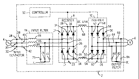
Referring to FIG. 1, a schematic is provided regarding a first exemplary power
converter 2 that is
coupled to a three-phase AC power source 4 and a three-phase load 6. In the
present
embodiment, the power converter 2 is a current source inverter (CSI) that, as
described in further
detail below, includes a first stage that is a rectifier 8 and a second stage
that is an inverter 10.
The three-phase AC power source 4 is intended to be representative of a
variety of AC power
sources that could provide first, second and third phases of AC electrical
power to the power
converter 2 including, for example, a utility/power line or other voltage
source, and potentially
can include three separate voltage sources. The AC power source 4 in the
present embodiment is
an AC voltage source albeit, in other embodiments it could be another type of
power source such
as an AC current source. Additionally, in the embodiment shown, the load 6 is
a three-phase AC
motor (e.g., an induction or synchronous motor), and can be modeled as three
resistors
respectively in series with three inductors (not shown) that represent three
different windings of
the motor, respectively. However, the load 6 is also intended to be
representative of other three-
phase AC loads including, for example, other electromechanical machines.
Further as shown in FIG. 1, the rectifier 8 of the power converter 2 includes
first, second and
third pairs of symmetric gate commutated thyristors (SGCTs) 12, 14 and 16,
respectively. The
SGCTs of each pair 12, 14 and 16 are coupled in series with one another
between first and
second nodes 18 and 20, respectively. Additionally, first, second and third
additional nodes 22,
24 and 26, which are respectively between the SGCTs of each of the first,
second and third pairs,
12, 14 and 16, respectively, are coupled to first, second and third input
ports 28, 30 and 32,
respectively, of the overall power converter 2. More specifically, the first,
second and third input
ports 28, 30 and 32 are respectively coupled to first, second and third input
contacts 38, 40 and
42, respectively, which together constitute an input contactor (or breaker or
other disconnect
device). The input contacts 38, 40 and 42 in turn are respectively coupled to
first, second and
CA 02577524 2007-02-07
third filter inductors 44, 46 and 48, respectively, which are respectively
coupled between the
respective input contacts and the respective first, second and third
additional nodes 22, 24 and
26, respectively.
During normal operation of the power converter 2, the rectifier 8 operates to
convert the three
phases of AC power received at the first, second and third input ports 28, 30
and 32 and
subsequently at the first, second and third additional nodes 22, 24 and 26
into DC power with
DC current output at the nodes 18, 20 (e.g., with currents of equal and
opposite polarities flowing
to/from the nodes 18, 20). The rectifier 8 achieves the AC to DC conversion by
way of
appropriate switching on and off (or pulsing on and off) of the pairs of SGCTs
12, 14 and 16 as
determined by a controller 50, which can be a microprocessor, programmable
logic device (PLD)
or other control device.
As for the inverter 10 it also is a PWM device that employs first, second and
third pairs of
SGCTs 52, 54 and 56, respectively, where the SGCTs of each pair 52, 54 and 56
are coupled in
series with one another between first and second nodes 58 and 60. The pulsing
on and off of the
SGCTs of the inverter 10 also is governed by the controller 50. Further,
fourth, fifth and sixth
additional nodes 62, 64 and 66, respectively, are positioned respectively
between the SGCTs of
each pair 52, 54 and 56, and respectively constitute (or in alternate
embodiments are respectively
coupled to) first, second and third output ports of the power converter 2 at
which are provided
three phases of outputs to the load 6.
Additionally as shown, the first and second nodes 18 and 20, respectively, of
the rectifier 8 are
coupled to the first and second nodes 58 and 60, respectively, of the inverter
10 by way of first
and second inductors 68 and 70, respectively, which are magnetically coupled
to one another so
as to be mutually inductive. The inductors 68, 70 serve as chokes allowing DC
current to pass
between the rectifier 8 and the inverter 10, while at the same time filtering
out (at least some) AC
power, and thus the inductors can be considered to form a "DC link" of the
power converter 2.
By virtue of the pulsing on and off of the pairs of SGCTs 52, 54 and 56, the
DC power provided
by way of the DC link is converted into the AC output power provided at the
fourth, fifth and
sixth additional nodes 62, 64 and 66 and output by the power converter 2.
Further as shown, the power converter 2 also has six capacitors. First, second
and third
capacitors 72, 74 and 76, respectively, couple the respective first, second
and third additional
nodes 22, 24 and 26 of the rectifier 8 to a common node 71. Together with the
inductors 44, 46
6
CA 02577524 2007-02-07
and 48, the capacitors 72, 74 and 76 form an input filter 78 that filters
extraneous power (e.g.,
power lacking the desired AC characteristics) provided from the input contacts
38, 40 and 42
before it reaches the rectifier 8. In addition to the capacitors 72, 74 and
76, the power converter
2 also has fourth, fifth and sixth capacitors 80, 82 and 84, respectively,
which couple the
respective fourth, fifth and sixth additional nodes 62, 64 and 66 of the
inverter 10 to a common
node 81 and serve as an output filter.
As discussed above, in at least some circumstances, the AC power source 4 can
experience
failures or other events that result in the disruption of power being supplied
to the power
converter 2. When such disruption occurs, typically one or more of the filter
capacitors 72, 74
and 76 are at such times partly charged and are storing some energy. For at
least the reasons
discussed above, it is desirable for these filter capacitors to be discharged
and, in particular, to be
discharged quickly. FIG. 2 provides a flow chart 100 showing exemplary
operational steps of
the power converter 2 as governed by the controller 50 that allow the power
converter 2 to
perform "active discharging" of the filter capacitors 72, 74 and 76 in such a
manner that the filter
capacitors are discharged much more rapidly than would otherwise be the case
in connection
with the operation of conventional power converters.
As shown in FIG. 2, the active discharging technique in at least some
embodiments is a multi-
step energy transfer process. During normal operation of the power converter
2, the controller
50 (by way of voltage/current sensors, not shown) monitors the voltages across
the filter
capacitors 72, 74 and 76 to detect whether a line loss (or other disruption in
the power being
supplied by the AC power source 4) has occurred, as represented by a step 102.
Upon detecting
that a line loss has occurred, at a step 104, the power converter 2/controller
50 enters a "transient
protection mode" at a step 106. Upon entering the transient protection mode,
the controller 50
continues to monitor the voltages across the filter capacitors 72, 74 and 76
to detect whether the
voltages across the filter capacitors have reached a DC state, as represented
by a step 108. If at a
step 110 it is determined that none of the filter capacitors 72, 74 or 76 any
longer has any AC
voltage, and that one or more of the filter capacitors has a DC voltage, the
controller 50 then
initiates the active discharging process by proceeding to a step 112
(otherwise, the controller
cycles between steps 108 and 110). In particular, upon the commencement of the
active
discharging process at step 112, the controller 50 of the power converter 2
commands the input
contacts 38, 40 and 42 (which are closed during normal operation of the power
converter) to
7
CA 02577524 2007-02-07
open, and then awaits confirmation of this status at a step 114. To the extent
that confirmation is
not obtained, the power converter 2 repeats steps 112 and 114.
Once the confirmation is obtained, the controller 50 then proceeds to a step
116, at which the
controller directs the operation of the rectifier 8 and inverter 10 so as to
cause pre-discharging of
any trapped energy within the DC link (e.g., the inductors 68, 70) of the
power converter 2 into
the load 6. Such pre-discharging is desirable (and, at least in some
embodiments, is necessary)
in order to make room in the DC link, in terms of the energy storage capacity
of the inductors 68,
70, for the energy stored in the capacitors 72, 74 and 76. In particular, it
is desirable to pre-
discharge the inductors 68, 70 of the DC link in case there is any DC current
trapped from free-
wheeling. This is accomplished by causing the pairs of SGCTs 12, 14 and 16 of
the rectifier 8 to
enter a disconnect mode such that the DC link is effectively disconnected from
the input contacts
38, 40 and 42 (and the capacitors 72, 74 and 76) so that energy transfer
therebetween is entirely
or substantially precluded, and producing maximum positive DC voltages within
the inverter 10.
In the present embodiment, the disconnect mode is a free-wheeling mode (e.g.,
achieved by
short-circuiting the pairs of SGCTs 12, 14 and 16), albeit effective
decoupling of the DC link
from the input contacts can be achieved in other manners, for example, when
other types of
power converters are employed as discussed in further detail below.
While the rectifier 8 is operated in the disconnect mode, the controller 50
additionally controls
the SGCTs 52, 54 and 56 of the inverter 10 to fire in a normal PWM pattern.
Assuming that the
load 6 is a motor, and further assuming that the motor flux is known, the
inverter 10 fires at a
firing angle to produce maximum torque. This results in the maximum inverter
DC link voltage,
such that the inductors 68, 70 are discharged at the maximum possible rate.
However, if the
motor flux is not known, the inverter 10 injects DC current into the motor as
is normally done in
the magnetizing interval during a start. Since the motor voltage and DC link
voltage are low,
this results in a relatively slow discharge (e.g., 100ms), mainly through
device, DC link and
motor losses.
In any event, as indicated by a step 118, the controller 50 monitors whether
the DC link current
is zero or sufficiently close to zero (e.g., by way of current monitors, not
shown) and whether a
given (arbitrary) time period has elapsed (e.g., 1 second) since the pre-
discharging at step 116
began. Until at least one of these conditions is met, the power converter 2
continues to cycle
between steps 116 and 118, such that the pre-discharging continues. The time-
out condition is
8
CA 02577524 2007-02-07
designed to allow the controller 50 to leave step 116 in the event there is
some type of
malfunction such that the DC link current apparently is not progressing to
zero.
Once one or both of the conditions of step 118 are met, the power converter 2
advances to a step
120, in which the rectifier 8 and inverter 10 are operated in a manner
resulting in most (or all) of
the energy stored in the filter capacitors 72, 74 and 76 (e.g., associated
with DC voltages existing
across one or more of those capacitors) being transferred into the inductors
68, 70 of the DC link.
More specifically, after the inductors 68, 70 of the DC link have been pre-
discharged, the
controller 50 causes the inverter 10 to enter a disconnect mode such that the
DC link is
effectively decoupled from the nodes 62, 64 and 66 (e.g., from the output
terminals of the power
converter 2). In the present embodiment, the disconnect mode of the inverter
10 is a free-
wheeling mode (e.g., in which one of the SGCT pairs 52, 54 and 56 are short-
circuited), albeit in
other embodiments the DC link could be effectively decoupled from the output
nodes/ports in
other manners.
While the inverter 10 is operating in the disconnect mode, the controller 50
further causes the
rectifier 8 to operate in a particular manner such that the DC link becomes
available as a sink for
the energy in the capacitors 72, 74 and 76. As discussed in further detail
below, the particular
manner in which the rectifier 8 operates can be significant in determining
whether all of the
voltages across each of the filter capacitors 72, 74 and 76 are largely or
substantially discharged
instead of only one of those voltages being discharged.
Referring additionally to FIGS. 3 and 4, in the present embodiment, the
controller 50 regulates
the speed at which the filter capacitors 72, 74 and 76 discharge their energy
into the inductors 68,
70 of the DC link by adjusting the DC output voltage of the rectifier 8
through the modulator
reference vector. Exemplary processing steps of the controller 50 in achieving
control of the
rectifier 8 (more specifically, the pulsing on and off of the SGCTs 12, 14 and
16 of the rectifier)
are shown in simplified form in a block diagram 130 of FIG. 3 and in further
detail in a block
diagram 140 of FIG. 4.
As shown in FIG. 3, based upon the information received concerning the
voltages on the filter
capacitors 72, 74 and 76, the controller 50 first performs a discharge control
step 132 in which a
rate of discharging is adjusted to suit the capability of the digital control
system and the
switching frequency of the SGCTs 12, 14 and 16 (or other power electronic
devices) of the
rectifier 8. Fast discharging typically requires a fast switching frequency
and a high sampling
9
CA 02577524 2007-02-07
rate. Additionally, the controller 50 in performing the discharge control step
operates as a
vector-oriented system that aligns itself with the vector formed by the three-
phase capacitor
voltage resulting from the three voltages of the capacitors 72, 74 and 76.
This type of scheme is
necessary because the filter capacitors 72, 74 and 76 are often wye-connected,
and the neutral
point is not available. Attempting to bring the individual line-to-line
voltages to zero separately
does not always ensure that the line-to-neutral voltage of each of the
capacitors is zero.
However, a full discharge can be accomplished by discharging the capacitors as
a three-phase set
as is done with this scheme.
The result of the discharge control step 132 is a two-component reference
vector 138. After the
discharge control step 132 is performed, the controller 50 additionally
performs a modulation
step 134 to generate gating signals 136. As described in more detail below
with respect to FIG.
4, in at least one embodiment, this modulation step 134 can involve
application of a variable
modulation index (using bypass) trapezoidal PWM pattern with delay angle
control. However,
in alternate embodiments, a wide variety of other types of modulation steps or
procedures can be
employed including, for example, other (non-trapezoidal) types of space vector
modulation, on-
line modulation techniques and carrier-based modulation techniques, among
others.
In the present embodiment, more particularly, the gating signals 136 are
varied as a function of
the three-phase capacitor voltage vector magnitude given by equation (1):
Vc, max = Max(Vab , Vbc ~ Vca )
Bc = tan-1 VY
Vx (1)
The gating reference frame is determined from (1) without using a Phase Locked
Loop (PLL).
Unfiltered voltage feedback inputs are used to avoid delays in the feedback
loop. The outputs
provided by this step are the six gating signals 136 that are respectively
applied to the respective
SGCTs of the rectifier 8. In the present embodiment, the switching frequency
of the PWM
pattern is 500Hz, albeit other frequencies can also be used.
FIG. 4 shows in more detail exemplary process steps that, in at least some
embodiments, can be
performed by the controller 50 in controlling the rectifier 8 so that energy
from the filter
capacitors 72, 74 and 76 is transferred to the inductors 68, 70 of the DC
link. As shown, the
controller 50 receives information concerning the voltages on the three filter
capacitors 72, 74
and 76 (which is unfiltered feedback information) and, at a step 142, performs
a three-to-two
CA 02577524 2007-02-07
transformation to arrive at a two-component voltage 144 having components V,
and Vy. At a
step 146, the controller 50 then further converts the two-component voltage
144 from its
Cartesian form into a polar voltage 148 having a magnitude Vc and an
associated angle 0,
Further as shown, the controller 50 at a step 150 also makes a determination
as to which of the
voltages on the three capacitors 72, 74 and 76 is the largest. Additionally,
while not necessary in
alternate embodiments, in the present embodiment the controller 50 then
normalizes the voltages
in relation to the rated voltage, so as to determine a maximum normalized
voltage magnitude
V,ma, and to allow for subsequent calculations to be performed using per unit
values.
This maximum voltage magnitude V. max in turn is used to determine two
quantities, a firing
angle a and a modulation index 157. More particularly, at a step 152, the
controller 50 in the
present embodiment generates the firing angle a as a function of 30 multiplied
by the square of
the maximum voltage magnitude Vcmax. The firing angle a in turn is added to
the capacitor
voltage angle 148 in a summing operation 154 to arrive at a reference angle
155. Additionally,
at a step 156, the controller 50 calculates the modulation index 157 as a
function of 0.2
multiplied by the maximum voltage magnitude Vcmax taken to the fourth power.
The modified
polar voltage 155 and the calculated modulation index 157 together can be
viewed as
constituting one embodiment of the reference vectors 138 of FIG. 3. Both the
reference angle
155 output from the summing operation 154 and the calculated modulation index
157 are utilized
by the controller 50 to perform a trapezoidal space vector modulation step
158, which in turn
results in the generation of six gating signals 160 that are respectively
provided to the respective
SGCTs of the rectifier 8.
Initially, the maximum voltage magnitude Vcmax could be more than 100% due to
the behavior of
the line reactors (e.g., the inductors 44, 46 and 48) during the opening of
the input contacts 38,
40 and 42. For this reason, in the present embodiment the delay/firing angle a
starts at 75 . This
large firing angle reduces the device voltage stress, and is also effective in
`throttling' the rate of
energy flow to the inductors 68, 70 of the DC link. The rate of energy flow
into the DC link is a
function of the DC output voltage of the rectifier 8, which in turn is a
product of the capacitor
voltage magnitude, modulation index 157, and cosine of the firing angle a. A
relatively slow
and controlled process is desirable since it allows the transfer to take place
at a rate that is
compatible with the speed of the sampled-data system, and it allows for a low
switching
11
CA 02577524 2007-02-07
frequency. As discussed above, the delay/firing angle a is proportional to the
square of the
maximum voltage magnitude V,,,,,a,,, such that the angle is very small when
the voltage is small.
Also in the embodiment of FIG. 4, the modulation index 157 is adjusted to
reduce the slope of
the capacitor voltage as the discharging nears completion. A small slope is
desirable in order to
prevent "overshooting," where the capacitor voltage goes through zero, and
starts charging to the
opposite polarity. Thus, the modulation index 157 is adjusted to be
proportional to the capacitor
voltage raised to the fourth power. A very non-linear function is appropriate
because the DC
current is near its maximum when the capacitor voltage nears zero, making the
potential
discharge rate very fast. When the capacitor voltage is near enough to zero,
the rectifier 8
immediately freewheels to trap the energy in the inductors 68, 70 of the DC
link and stop the
capacitor voltage discharge process. If (e.g., in alternate embodiments) the
process were not
stopped, some of the energy in the DC link would return back to the
capacitors. Due to the
choice of reference frame and control scheme used, this energy would then need
to be removed.
In practice, if the speed of discharging is fast, and the capacitor voltage
overshoots, the process
goes through a series of oscillations.
As mentioned above, the particular type of modulation that is performed can
vary depending
upon the embodiment. Further, while the reference angle 155 and modulation
index 157 are, in
the present embodiment, calculated by way of particular formulas (e.g., those
associated with
steps 152 and 156), these manners of calculating angle 155 and index 157 (and,
indeed, any
reference vector(s) provided for modulation) can be varied in alternate
embodiments. For
example, the firing angle a in some alternate embodiments could be zero and/or
the manner of
calculating the modulation index 157 could employ other exponential functions.
In the present
embodiment, and in most embodiments, a goal of the particular algorithms that
are used is to
limit the voltages that occur across the switching devices/bridge
notwithstanding the possible
existence of relatively high voltages appearing across the input filter
capacitors.
Referring again to FIG. 2, as the energy stored in the filter capacitors 72,
74 and 76 is being
discharged into the inductors 68, 70 of the DC link at step 120, the
controller 50 repeatedly or
continually monitors whether the voltages on the filter capacitors have
reached (or come close
enough to, e.g., within a threshold of) zero, at a step 122. The determination
of whether the
voltages of the filter capacitors 72, 74 and 76 have reached zero, which is
indicative of whether
the energy stored in the capacitors has been sufficiently transferred to the
DC link, again is
12
CA 02577524 2007-02-07
typically based upon an evaluation of the overall three-phase voltage of the
three filter
capacitors. Until such time as the filter capacitor voltages have reached
zero, the controller 50
cycles between steps 120 and 122. Once the voltages on the filter capacitors
have reached zero,
the controller 50 proceeds from step 122 to a step 124, at which the
controller 50 then operates
the rectifier 8 and inverter 10 in such a manner that the energy trapped in
the DC link (obtained
from discharging the input filter capacitors) is discharged into the load 6
(e.g., the motor).
More particularly, while during the execution of step 120 the pairs of SGCTs
52, 54 and 56 of
the inverter 10 are operated in a disconnect (e.g., free-wheeling) mode and
the pairs of SGCTs
12, 14 and 16 of the rectifier 8 are controlled in accordance with a process
such as those
described with respect to FIGS. 3 and 4, during the execution of the step 124
the pairs of SGCTs
12, 14 and 16 of the rectifier 8 are operated in a disconnect (e.g., free-
wheeling) mode and the
pairs of SGCTs 52, 54 and 56 of the inverter 10 are operated in the same
manner as described
above with reference to step 116 such that the energy within the inductors 68,
70 of the DC link
is discharged into the load 6 (e.g., motor). Additionally, as indicated by a
step 126, the controller
50 monitors whether the DC link current is zero or sufficiently close to zero
(e.g., below 2% of
its initial value) and whether a given time period has elapsed (e.g., 1
second) since the
discharging of step 124 began. Until at least one of these conditions is met,
the controller 50
continues to cycle between steps 124 and 126. Once one (or both) of these
conditions is met,
however, the controller 50 stops the active discharging process at a step 128
and, in particular,
stops the gating of the SGCTs of the inverter 10, and then closes the input
contacts 38,40 and 42
(at least when power from the source 4 is restored).
The above-described active discharging process involves transferring the
energy in the filter
capacitors 72, 74 and 76 to the inductors 68, 70 of the intermediate DC link
and then
subsequently dissipating that energy in the motor or other load. For this
process to achieve the
desired transfer of energy, it is necessary that the inductors 68, 70 be (at
least temporarily)
capable of storing the energy received from the capacitors, and consequently
it is necessary that
the inductors be capable of handling the DC currents associated with the
storage of that energy.
The maximum DC currents that the inductors 68, 70 need to be able to handle in
a given case
when line loss occurs can be calculated as follows. To begin with, the total
energy stored in
each capacitor is
13
CA 02577524 2007-02-07
E = 1 C.V2
2 (2)
where C is the line-to-neutral capacitance and V is the DC line-to-neutral
voltage. The total
stored energy in the three filter capacitors 72, 74 and 76 and transferred to
the DC link is given
by:
Etota! = 21C(Va2 +Vb2 +Vc2)- 2L I'dcldc2
(3)
where Va, Vb and Vc represent the voltages of the filter capacitors 72, 74 and
76, respectively,
after the input contacts 38, 40 and 42 have been opened. Assuming that all of
the energy from
the line filter capacitors is transferred to the inductors 68, 70 of the DC
link, the resulting DC
current would be:
C(Va2 +Vb2 +Vc2)
I dc =
Ld, (4)
It can further be shown that the maximum energy is stored when the
utility/source 4 is
disconnected at the peak of one of the phase voltages. When this occurs, one
of the filter
capacitors 72, 74 or 76 would have a DC voltage of +1 per unit (if the base
voltage is defined to
be the peak line-to-neutral voltage) and the other two phases would have a DC
voltage of -0.5
per unit. Therefore the maximum DC link current in per unit values can be
determined by the
per unit line filter capacitance and per unit DC link inductance to be:
3C
I dc _ 2
Ldc
(5)
For a PWM rectifier, typical sizes of the filter capacitors and DC link
inductors are 0.4 per unit
and 0.6 per unit respectively. This combination would result in a peak DC
current of 1 per unit,
which would be acceptable. Additionally, power converters with input filter
capacitors larger
than 0.5 per unit and smaller DC link inductors of 0.5 per unit would result
in a DC link current
of 1.22 per unit. Although this is large, it can still be acceptable because,
in a running power
converter/drive, the peak DC current can momentarily exceed this value due to
ripple, and high
transient output torque.
While preferably the DC link (e.g., the energy storage capacity of the
inductors of the DC link) is
large enough to allow for all residual input filter capacitor energy to be
transferred to the DC link
in one step, in alternate embodiments the DC link is not large enough for all
such energy to be
transferred at once, and consequently the energy must be transferred in
multiple steps. In such
14
CA 02577524 2007-02-07
alternate embodiments, the steps of the flow chart 100 would be modified
somewhat such that
the sequence of steps involving the transferal of energy from the capacitors
to the DC link and
subsequently to the motor/load would be repeated on two or more occasions. The
flow chart
would also include one or more steps relating to the detection of whether a
particular finite
amount of capacitor voltage/energy had been dissipated rather than simply (as
in the case of step
122) relating to detecting whether the capacitor voltages had been reduced to
zero.
Although FIGS. 1-4 show exemplary embodiments of power converters and/or the
active
discharging procedures performed by those power converters, the present
invention is also
intended to encompass other embodiments of power converters and active
discharging
operations. To begin with, while the above description concerns drives, the
present invention is
also applicable with respect to power converters other than drives (e.g., the
present invention
could pertain in some embodiments to a power converter that is used as a
variable voltage,
variable frequency power supply for a passive load). Also, while the above
description concerns
three-phase power converters, the present invention is also applicable with
respect to power
converters that only are single-phase, or have a multiplicity of phases other
than three (e.g., two-
phase or four-phase power converters). More particularly, the present
invention is applicable to
any power converter that has a DC link coupling two stages of power conversion
device such as
a rectifier and an inverter.
Additionally for example, while the power converter 2 is a CSI power
converter, the present
invention is also intended to encompass voltage source inverter (VSI) power
converters that
employ capacitors rather than inductors in the DC link sections of the power
converters. Also,
while the CSI power converter discussed above is operated in free-wheeling
modes as its
disconnect modes, in alternate embodiments procedures other than free-wheeling
can be
employed to decouple/disconnect the DC link from the input and output
terminals of a power
converter at appropriate times (e.g., can be employed as other disconnect
modes of operation).
This will often be the case when power converters other than CSI power
converters are involved.
For example, a disconnect mode involving open-circuiting of switching devices
rather than
short-circuiting of switching devices (e.g., as in free-wheeling) would
typically be employed in
conjunction with VSI power converters.
Additionally, in alternate embodiments, the power converters can employ
switching devices
other than SGCTs, for example, integrated gate commutate thyristors (IGCTs) or
insulated gate
CA 02577524 2007-02-07
bipolar transistors (IGBTs). Further, while in the above-described embodiment,
each of the
rectifier and the inverter includes six switching devices, in other
embodiments other types of
rectifiers and/or inverters having different numbers or
interconnections/orientations of devices
can also be employed (e.g., a rectifier having eighteen switching devices
rather than six
switching devices could be employed). Also, while the above-described
embodiments relate to
achieving discharging of energy stored on the input filter capacitors of a
power converter, the
present invention is also intended to encompass other embodiments in which
energy stored on
other devices (e.g., inductors) is actively discharged.
Further, in three-phase embodiments such as that described above, each of the
AC power source
and the load can be either wye-connected (Y-connected) devices or delta-
connected (A-
connected) devices. Additionally, while in the embodiment described above both
the input filter
capacitors and the output filter capacitors are Y-connected, in alternate
embodiments one or both
sets of filter capacitors can be A-connected. Further, the present invention
is also intended to
encompass other operations/calculations performed by one or more controllers
of (or in
association with) a power converter in order to achieve the active discharging
of stored energy
that is retained after a disruption of input power to the power converter. It
will be understood
that, typically, the controller 50 (or other controller of the power
converter) will include or be in
communication with one or more memory devices that store program(s) for
governing the
processing and control operations of the controller, such as those described
with respect to
FIGS. 2-4.
Turning now to FIGS. 5-8, several graphs (FIGS. 5-7) are provided showing how
different
signals associated with one exemplary implementation of the power converter 2
could vary with
time during a disruption in the input power being provided to the power
converter, and additional
graphs (FIG. 8) show by comparison how some of the signals would otherwise
vary in the
absence of such an active discharging procedure. These graphs are generally
intended to
demonstrate how, in at least some embodiments of the invention, active
discharging of residual
voltage/stored energy on input filter capacitors of a power converter (or
possibly other energy
storage devices) is achieved in a rapid manner such that transient voltages
are minimized upon
reapplication of input power to the power converter (e.g., upon recovery of
line voltage), and
such that delays in the operation of the power converter related to the
discharge of the residual
voltage/stored energy are minimal.
16
CA 02577524 2007-02-07
Referring to FIG. 5 in particular, first, second, third and fourth graphs 162,
164, 166 and 168,
respectively, show exemplary time variation of the voltage across one of the
filter capacitors
(e.g., any of the capacitors 72, 74 and 76 of FIG. 1), the inverter DC link
voltage (e.g., the
voltage existing across the nodes 58 and 60 of FIG. 1), the rectifier DC link
voltage (e.g., the
voltage existing across the nodes 18 and 20 of FIG. 1), and the current
through the DC link (e.g.,
through one of the inductors 68, 70), respectively. FIG. 5 in particular shows
exemplary time
variation of these quantities between a first time 170 at which a line
loss/input power supply
disruption occurs and a second time 172 at which the input power supply
recovers.
Further as shown in FIG. 5, after the line loss occurs at the first time 170,
at a subsequent time
174 the DC link current shown by the graph 168 begins to decline due to pre-
discharging. Next,
between a time 176 and a time 178, the controller causes the discharging of
the energy stored in
the filter capacitors into the DC link, which corresponds to step 120 of FIG.
2. During this time
period, the capacitor voltage (graph 162) approaches zero, the DC link current
(graph 168)
increases and the rectifier DC link voltage (graph 166) experiences pulsing as
the SGCTs of the
rectifier 8 are pulsed on and off. Subsequent to the time 178, between that
time and a time 180,
the energy in the DC link is further discharged to the load/motor via the
inverter, as corresponds
to step 124 of FIG. 2. Correspondingly, graph 164 shows variation in the
inverter DC link
voltage during this time period. After time period 180, the active discharging
process is
complete and the input contacts can be closed upon (or in anticipation of) the
recovery of the
input power at time 172.
Turning to the remaining FIGS. 6-8, FIG. 6 shows in greater detail (e.g.,
magnifies) respective
portions of each of the graphs 162, 164, 166 and 168 (now labeled graphs 162',
164', 166' and
168', respectively) that are associated with a time interval extending from
just prior to the time
176 to just subsequent to the time 178. FIG. 7 in contrast shows modified
versions of the graphs
162 and 168 (now labeled graphs 162" and 168", respectively) that encompass
longer periods of
time prior to the time 170 and subsequent to the time 172 of FIG. 5. Further,
FIG. 7 provides
two additional graphs 182 and 184 that respectively show the signal provided
by the controller
(e.g., the controller 50) to the input contactor (e.g., the contactors 38, 40
and 42) and the status of
the input contactor. The graphs 182 and 184 in particular demonstrate that
there is a time lapse
between a time 186 at which the controller commands the input contacts to open
and a time 188
17
CA 02577524 2007-02-07
at which the contacts actually open, which occurs at or just prior to the time
174 at which pre-
discharging of the DC link begins.
Finally, FIG. 8 provides graphs 190, 192, 194 and 196 that respectively
correspond to graphs
162", 168", 182 and 184 of FIG. 7, respectively, in terms of showing the time
variation of filter
capacitor voltage, DC link current, input contactor command timing, and input
contactor
operation. However, FIG. 8 illustrates exemplary operation of the power
converter 2 in the event
that the active discharging procedure described above was not performed
subsequent to the
occurrence of a power supply disruption. As shown, in such case the DC link
current (graph
192) would decrease over time after the power supply disruption, but any
nonzero filter capacitor
voltage 198 would largely if not entirely remain constant over time. As a
result, upon the
recovery of the power supply at a time 200, there would typically be
considerable, undesirable
transient voltage variation.
It is specifically intended that the present invention not be limited to the
embodiments and
illustrations contained herein, but include modified forms of those
embodiments including
portions of the embodiments and combinations of elements of different
embodiments as come
within the scope of the following claims.
18