Note : Les descriptions sont présentées dans la langue officielle dans laquelle elles ont été soumises.
CA 02578496 2007-02-28
WO 2006/033893 PCT/US2005/032573
ENHANCED BANDWIDTH DATA ENCODING METHOD
PRIORITY BENEFIT AND CROSS REFERENCE TO RELATED APPLICATIONS
This application is related to the following commonly owned copending U.S.
Patent Applications:
Provisional Application Serial No. 60/611,220, "Enhanced Bandwidth Data
Encoding Method," filed
September 17, 2004, and
Utility Serial No. 11/201,220, "Enhanced Bandwidth Data Encoding Method,"
filed on August 10,
2005.
TECHNICAL FIELD
This invention deals with the encoding and transmission of data, and more
particularly with addressing
and timing techniques for systems using a multidimensional array of elements
that present or transmit
information to a user or reading system.
BACKGROUND INFORMATION
Data encoding algorithms find a rich application field in the realm of
electronic video displays,
particularly with respect to flat panel display systems. While in no way
limiting the present invention, or
associated prior art, to this application, it is instructive to tabulate the
features of such example applications to
illustrate how prior art has evolved and been applied. This approach is
followed in the discussion immediately
following.
The first illustrative example for the application of such encoding algorithms
is a direct-view flat panel
display system that uses sequentially-pulsed bursts of red, green, and blue
colored light emanating from the
display surface to create a full color image. The human visual system
effectively integrates the pulsed light
from a light source to form the perception of a level of light intensity. By
making an array of pixels (picture
elements on the video display) emit, or transmit, light in a properly pulsed
manner, one can create a full-color
display. A term commonly used to define this technique is called field
sequential color (hereafter, FSC), and
U.S. Pat. No. 5,319,491 (Selbrede) entitled "Optical Display," uses this
phenomenon as a basis for a flat panel
display and is incorporated by reference herein.
The gray scale level generated at each point on the display surface is
proportional to the percentage of
time the pixel is ON during the primary color subframe time, tcolor. The frame
rates at which this occurs are high
enough to create the illusion of a continuous stable image, rather than a
flickering one. During each primary
color's determinate time period, tcolor, one can dictate the shade of that
primary color by having its associated
pixel open for the appropriate fraction of tcolor. For example, producing 24-
bit encoded color requires 256 (0-
255) shades defmed for each primary color. If one pixel requires a 50% shade
of red, then that pixel will be
assigned with shade 128 (128/256 = 0.5) and stay on for 50% of tcojor. This
form of data encoding assumes a
constant magnitude light source to be modulated across the screen. Moreover,
it achieves gray scales by evenly
subdividing tolorinto fractional temporal components.
1
CA 02578496 2007-02-28
WO 2006/033893 PCT/US2005/032573
To generalize from this specific video-based application to a wider range of
suitable applications, it is
appropriate to define terms to be used throughout this disclosure. The
individual video pixels, which correspond
to array elements from the standpoint of the incoming data, serve to modulate
(by on/off gating) the light present
within the display screen. The light within the screen (the global quantity to
be modulated by gating at each
array element) is emitted at a deterniinate intensity for a determinate
duration. This physical effect, of known
intensity and duration, shall henceforth be termed a transmission pulse. It is
the quantity that will be modulated
by the encoding data within the array. The light illuminating the video
display, then, is a surrogate for a larger
class of quantifiable entities which can be mathematically encoded and
controlled using the methods disclosed
in this disclosure. Said quantifiable entities symbolized by the term
"transmission pulse" may not necessarily be
intensities of light energy, as the application range of the encoding method
is far broader than the field of video
displays.
Other technologies use FSC and pulse width modulation (hereafter, PWM) address
schemes to create a
projection-based system (as opposed to the direct-view system referenced
above). Such a projection-based
display is found in the Digital Light ProcessorTM (DLP) from Texas
Instruments, a patented projector system
which uses an array of micromirrors as disclosed in the patent for the Digital
Micromirror DeviceTM (DMD) (see
U.S. Patents 5,278,652 and 5,778,155, respectively). In the DMD, the mirrors
are tilted one way to reflect light
through a lens in a projection display system and tilted the opposite way to
prevent light from reflecting tlu-ough
the projection lens. By timing precisely when and for how long the mirrors are
oriented to reflect light, the
DMD reflects the correct shade, or brightness, of a either a constant primary
light source or a white light source
that is filtered through use of a continuously rotating color wheel. The
encoding strategy implemented in these
Texas Instruments devices divides the cycle time into unequal fractions, as
opposed to the equal duration time
slice strategy disclosed for the direct-view device in Selbrede. The unequal
fractional durations are temporally
proportioned as ascending powers of two (e.g., the second fraction is twice
the length of the first; the third
fraction is twice the length of the second, up to the largest fraction
contemplated).
SUMMARY
The present invention codifies a method of encoding data for applications such
as, but not limited to,
video display systems. Its utility is most obvious for video systems that, for
example, incorporate methods for
pulse width modulating frames of video data to control both input
(illumination) light sources and the individual
pixels comprising a spatial light modulator (SLM) composed of an array of
pixel elements that are addressable
in a row by row, and/or subarray by subarray, fashion. This encoding method
can also apply to an array of SLM
pixels where the state of each pixel may or may not be controlled by unique
transistors or other active switching
devices. The pixels in the array are addressed in a subarray by subarray
fashion for turning ON the pixels (i.e.
transmitting, reflecting, or emitting light). These subarrays may consist of
one row, some number of rows, or all
rows of the array. The entire array, or subarray of several rows, of pixels
can also be simultaneously set to the
same state (ON or OFF) during a screen refresh or reset. During the addressing
of the array of pixels, the light
sources used to transmit light through the pixels are controlled
independently.
2
CA 02578496 2007-02-28
WO 2006/033893 PCT/US2005/032573
The present invention would enhance the encoding of information being directed
toward a system
lending itself to such enhancement, such as, for example, a video display
device composed of optical shutters
that use frustrated total internal reflection (TIR) to create a transmissive
display that produces color by the
method of FSC. The example display system referenced earlier (Selbrede) is
known as the Time Multiplexed
5' Optical Shutter (TMOS). However, the present invention can also apply to
other display architectures, such as
those incorporating pulsed light sources and optical transmissive or
reflective elements, or pixels, whose light
properties originate from said pulsed light sources. The domain of
applicability for the present invention
extends far beyond video display devices, which are used herein for
illustrative purposes.
The present invention is particularly well suited to application within the
TMOS example already
described, since TMOS, within its utility range, uses a one-part per pixel
architecture whereby the full color
spectrum is transmitted through each pixel. Many display systems use a three
part pixel (i.e. red, green, and blue
regions comprising subpixels that are spatially distinct one from another)
which combine in some proportion to
produce the desired color when viewed far from the screen. The light sources,
or lamps, that serve to illuminate
the TMOS system are controlled independently of the on-screen pixels, which
are actuated as required based on
program content. Consonant with the definition proposed at the outset, the
sequential activation of the primary
color light sources that illuminate the TMOS display constitute an example of
"transmission pulse" events. The
transmission pulse is spatially modulated by the controllable array of pixels
that permit or forbid coupling of the
light out of the display for propagation to the observer, who, over time and
pursuant to the principles of FSC,
perceives a color video image on the display surface.
Most encoding mechanisms for FSC-based systems presuppose some form of
bistable, memory, or
persistence effect, such as that disclosed, as one possible example among
many, in the patent filing "Simple
Matrix Addressing" (Derichs) which is hereby incorporated by reference in its
entirety. This memory effect
may or may not result from individual, and/or discrete, memory elements, such
as CMOS memory cells or
transistors. For example, one embodiment of TMOS posits that each pixel is a
microelectromechanical system
(MEMS) variable capacitor configured so that the separation between conductors
in each pixel's air gap can be
reduced during actuation from a default unactuated state during which no
voltage or charge is applied to the
pixel. In said example, applying a voltage across the capacitor forces the
upper electrode to approach the lower
electrode through Coulomb attraction, thereby reducing the air gap distance
while increasing the pixel's
capacitance. In this example, when a sufficient voltage, Vl, is applied, the
moving upper conductor layer will
contract to come into contact with the lower conductor layer (unless they are
separated by some solid dielectric)
in an effect known as the pull-in or snap-down. To release the contact between
the two conductors (or their
respective dielectrics) the capacitor voltage needs to reach a second voltage,
V2, that is less than VI. All
nonaddressed rows stay within the voltage range V2 < V< Vl, Thus, an addressed
row of pixels can be actuated
without changing the state of the pixels (or capacitors) in the nonaddressed
rows. This control method takes
advantage of the hysteretic nature of the pixels being variable capacitors.
The present invention is both
compatible with and suitable for application to this particular device.
3
CA 02578496 2007-02-28
WO 2006/033893 PCT/US2005/032573
The present data encoding invention is also applicable for other control
methods that, for example, can
alter the discharge rate of a row of pixel capacitors from high (when
addressing that row) to low (when not
addressing that row). Where suitable preconditions for applicability are met,
the present invention provides
significant utility in optimizing the encoding of data.
The foregoing has outlined rather broadly the features and technical
advantages of one or more
embodiments of the present invention in order that the detailed description of
embodiments of the present
invention that follows may be better understood. Additional features and
advantages of embodiments of the
present invention will be described hereinafter which form the subject of the
claims.
BRIEF DESCRIPTION OF THE DRAWINGS
A better understanding of the present invention can be obtained when the
following detailed description
is considered in conjunction with the following drawings, in which:
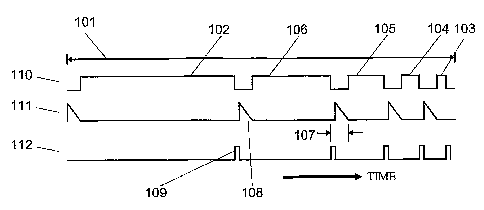
Figure 1 illustrates an example of using the present invention in a display
application, shows a timing
chart for a primary color subframe of a 5-bit color per primary binary
weighted FSC color scheme;
Figure 2 illustrates an example of using the present invention in a display
application, showing that the
time required for sequentially addressing an array of elements row by row is
composed of the times for loading
the data and then pulsing the rows for a time required to activate the pixels
in the addressed row;
Figure 3 illustrates an example of using the present invention in a display
application, showing a timing
chart and defining relevant terms for addressing a pixel array using FSC where
each subframe used to generate
shades of color is of equal time duration;
Figure 4 illustrates an example deployment of the present invention in a
display application, showing a
6-bit per primary binary FSC encoding method;
Figure 5 illustrates a 6-bit per primary dual binary encoding method that
includes transmission pulse
intensity control in accordance with an embodiment of the present invention;
Figure 6 illustrates an example timing pulse chart for the dual binary
encoding method to encode 6-bit
data in accordance with an embodiment of the present invention;
Figure 7 illustrates an algorithm for a data encoding scheme where the
transmission pulse is ON while
the data is loaded into and unloaded from the array in accordance with an
embodiment of the present invention;
Figure 8 illustrates an example of the present invention being deployed in a
display application,
showing a schematic of a 6-bit per primary hybrid binary FSC encoding method
that uses PWM lamp control at
full intensity;
I
Figure 9 illustrates an example of the present invention as deployed in a
display application, showing
an example schematic of the present invention deployed in a system using a 6-
bit per primary binary FSC
scheme with screen clear and PWM lamp control; and
Figure 10 illustrates an algorithm for a data encoding scheme where the
transmission pulse is OFF
while the data is loaded into and unloaded from the array in accordance with
an embodiment of the present
invention.
4
CA 02578496 2007-02-28
WO 2006/033893 PCT/US2005/032573
DETAILED DESCRIPTION
The present invention is a method of encoding data associated with an
arbitrarily-sized array of
elements the content of which may vary in value, of any dimension, where the
data is allowed to be presented in
different ways and at different times relative to when the data is loaded. The
array elements can present
multiple discrete states, two for binary, three for ternary, four for
quaternary, and so on. The input data stream
to be loaded to the array of elements generally contains more information than
can be presented, stored, or
transduced, by the array at any one instant in time. Therefore, data subsets
can be used in temporal succession
to present the full information set to the user. Either each individual data
subset presented in the array or the
subsequent temporal succession of data subsets presented in the elemental
array then provides the complete
information content of the input data stream within the application-specific
device in question. The time during
which each subset of information is sequentially presented in the array lasts
for some determinate duration
called the subset time. Each subset of data is normally expected to fill the
array and can be further decomposed
into subarrays that may be loaded and presented at different times. In some
video applications, the data being
transferred reflects only change in information content, such that the entire
array is not necessarily reloaded
during each subset time. The present invention applies to any such variation
as well as the expected core utility.
It is noted that the principles of the present invention are not to be limited
to the field of video display devices.
It is further noted that a person of ordinary skill in the art would be
capable of applying such principles to other
applications.
One possible application of the present invention is the transmission of a
frame of visual information
by use of FSC in a video display system consisting of a two-dimensional array
of pixels. In this real-world
example, a frame is a set of information that determines the color and
brightness of each pixel comprising the
video display being observed by the viewer. The frame is composed of multiple
data subsets, or subframes,
usually dictated by the number of primary colors to be mixed to create the
desired output (in this example, the
three so-called tristimulus colors - red, green, and blue -- are the most
commonly used primary colors). The
full-color information, then, is parsed into separate channels of data for
each primary color. Each subframe will
then encode different shades associated with the appropriate primary color
which-is a fraction of the primary full
intensity. These shades (which, in this data, are fractions of an irreducible
and discrete primary color) represent
the lowest subset of data for the display. Using FSC techniques, a desired
shade can be displayed by selectively
restricting the emission time of the primary color at a given pixel (array
element) for a determinate fraction of
time, the subset time, that is temporally proportional to its primary color
shade value. The total time allowed for
every full-color video frame is tfra1De = 1/(frames per second). In one
embodiment, the time allowed for every
constituent primary color is tcolor = tframe/.Ncolor, (101 of Figure 1), where
Nroior represents the number of primary
colors (generally set to 3 primaries for most video applications, but not
limited to 3, nor, for that matter, limited
to primary colors). For 60 fps and N.lor = 3 for red, green, and blue primary
lamps, time tco1or = 5.56 msec.
Figure 1 shows a representative example of a binary shade and timing sequence
for a display
application that deploys the present invention with 5-bit information per
primary color subframe 101, where
generically 101 represents a data subset time. This sequence would be repeated
for each primary color
comprising the FSC encoding scheme. The light source of the display is a
specific implementation of a general
5
CA 02578496 2007-02-28
WO 2006/033893 PCT/US2005/032573
transduction method applied to the elemental array. That is to say, when the
lights are on, the user can see the
information content of the encoded image on the display surface, and when they
are off, the user cannot see, or
read, the information (since no light is being emitted from the display
surface). Figure 1 shows that the
transmission pulse 110 is on at five different periods corresponding to the
five bits of information and the
corresponding five subsets. The most significant bit (hereafter MSB) 102 is
the longest in time, and the least
significant bit (hereafter LSB) 103 is the shortest in time. 103 lasts for 1/2
"1 of the total time light is emitted,
where n is the number of bits. The second most significant bit 1041asts for
2*103, the third most significant bit
105 lasts for 4*103, the fourth most significant bit 1061asts for 8*103, and
the fifth, or MSB 102, for 16*103.
Note again that the example provided is for illustrative purposes and is not
intended to limit the scope of
applicability or utility of the present invention.
A data subset of information presented in the element array takes some non-
zero array time 107 to be
loaded and stored 108 and some non-zero time to be unloaded and cleared 109
from the array due to the
temporal constraints of the array elements themselves and intrinsic latency of
the other physical components
comprising the system in question. The data can be loaded and cleared for all
elements simultaneously or
incrementally by handling a subarray of elements (such as one row of a two-
dimensional array) at a time. The
data is visually presented to the user independently of the loading pulse
sequence 111 and the unloading or'
clearing 112 pulse sequence as dictated in time and duration by the
transmission pulse 110, which is
unmodulated (full intensity) for the example disclosed at this point. The data
can either be presented as the data
is loaded 111 and cleared 112, or after all data loading of the array has been
completed.
For a sample display application using FSC, the transmission pulses 110
indicate when the light
sources are on. In Figure 1, the data loading pulse sequence 111 composed of
the pulses 108 represents when
the display pixels are actuated to ON, and the data clearing pulses 109 are
triggered by the clearing pulse
sequence 112 to turn the pixels OFF. Note that it is possible for the pulses
108 to trigger state changes among
the general array elements (ON, OFF, or others) provided there is enough time
available to do so. Thus, in the
display application example provided, the pulse sequence 111 can be composed
of pulses that turn some pixels
ON and then some pixels OFF, or vice versa.
Figure 2 depicts a more detailed breakdown of the data loading pulses 108 to
show one possible
method to load data to the array elements in a subarray by subarray fashion.
The present invention allows for
loading data for subarrays in one dimension (e.g. a row) or multiple
dimensions (e.g. rows and columns) of the
array at a time. The data loading pulses 201 occur before each element
subarray is activated, and they are often
temporarily stored, for example, in shift registers. When a pulse 201 is
fmished for the first elemental subarray,
the data is shifted to the first subarray by pulses 202. To load the data for
the entire element array, the loading
of data is continued by pulses 201 for data subarray two (203), data subarray
three (204), data subarray four
(205) and continuing for all 'm' data subarrays until data subarray 'm-l'
(206) and finally data subarray 'm'
(207) are handled. Each loading and shifting of the data takes a subarray time
208 to be completed for that
subarray. Thus, the total elapsed time to shift all data in a subset of
information is m*208 for the example of
equal duration for addressing each subarray.
6
CA 02578496 2007-02-28
WO 2006/033893 PCT/US2005/032573
Depending upon the control scheme underlying the element array, during a
single addressing event for
a given subarray the elements can (1) only be turned to some level ON state,
(2) only be turned to the OFF, or
(3) turned both to the proper ON state and OFF state before addressing the
next subarray. Each of these three
possibilities dictates a different bandwidth requirement to properly handle
the input data. It is noted that the
discussion below is for an embodiment in which the pixel elements are binary.
However, the principles of the
present invention may be applied to pixel elements that are ternary.
The maximum clock speed in each encoding scheme is calculated as Ncycles/107
where N~yeIeS is the
number of clock cycles per array address. N~ycleS is equal to Neiements/(input
bits per clock cycle) where Nelements is
the number of elements in the array. Consider the application of the present
invention to a representative video
display composed of Nro, number of rows and Nco1 number of columns of pixels.
If Nco1= 1024 and NroW = 768,
then Nelements = NroWN~ol. If the data is input at 32 input bits per clock
cycle, then these parameters produce Ncycles
= 24,576. The clock speed required for this FSC display application is roughly
determined by the time 107
allowed to address the display (assuming row by row addressing). For example,
if 107 = 300 sec, the
maximum required clock speed is approximately Ncycles/107 = 82 MHz. The peak
bandwidth (BW) is related to
the clock speed as BW = (bits per clock cycle)(max. clock speed). For the
current example with 32 bits per
cycle, the peak BW is 2.6 Gbit/sec. The utility inherent in the present
invention is that it minimizes bandwidth
by maximizing 107 and/or making it suitably variable.
EQUAL TIME ENCODING
The conceptually simplest (but far from most bandwidth-efficient) encoding
scheme would specify that
each subset time be of equal duration. If each subarray is of equal size, then
the subarray times are also equal.
In this case, the array time 311 can be solved as 311 = 310/Nsnbset where
Nsnbset is the number of subsets and 310
is the data set time. The corresponding subarray time (208 of Figure 2) in
this case is calculated to be
311/Nsnba,.y, where Nsnbanay is the number of subarrays per subset.
Figure 3 shows a schematic for the equal time subframe FSC application for a
display where the time
required to move along the slope of the parallelograms is the time, 107, to
address all pixels of a two-
dimensional row by column array. The part of the parallelograms that is
nonshaded (in this case the entire part
of each parallelogram) indicates the time at which the transmission pulse is
ON. For example, to create 6-bit
color per primary there are 65 = 64 + 1 subsets 305 (26 = 64). Therefore,
assuming in this example three
primary color lights, 302, 303, and 304, sequentially providing three separate
transmission pulses, there are
65*3 = 195 total subsets 305 in this application that fit within the frame
time 301. One suitable approach to
handling equal time encoding for a FSC display would be to turn all pixels ON
only once during each primary
color time 310 at the appropriate point within the subset to achieve the
desired shade. Then during the last
addressing of the array at the end of 310, every pixel will be turned OFF when
its subarray is addressed. This
corresponds to an articulated individual ON point and a common synchronous OFF
point. The opposite
approach is also quite feasible, wherein every pixel with non-zero data
content is initially turned ON, with each
7
CA 02578496 2007-02-28
WO 2006/033893 PCT/US2005/032573
pixel being individually turned OFF at the appropriate time during 310. In
this last instance, a common
synchronous ON point is juxtaposed with an articulated individual OFF point.
Using for illustrative purposes a video display application for deploying the
present invention, consider
that for an equal time FSC display application (60 fps, N.otor = 3), 311 =
310/65 = 168 sec (where 65 is based
on 6-bit color (26) plus 1) and with NroW = NsõbaraY = 768 the subarray time
is 219 nsec. In such an embodiment,
the time to address the array 311 is the same as the LSB time so that the
amount of time that the transmission
pulse (e.g. light source) is on for the first row is the same as for the last
row. This is the reason there are 65
subsets 305 within 310 instead of 64, as it assures the color shade generated
by pixels in the top (first) row is the
same as from those in the bottom (last) row. During the subarray time one is
able to turn all desired pixels in a
=
subarray either ON or OFF. The main clock speed required for this equal subset
time FSC embodiment (Nrow
,ot = 1024) is 289 MHz, corresponding to a peak bandwidth of 9.2 Gbit/s for a
32 bit-deep input to each
768, Nc
subarray.
1. FULL BINARY ENCODING
Figure 4 depicts the timing sequence for implementing a binary encoding scheme
using 6-bits as an
example. The advantage of this method is that it decreases the bandwidth
required to implement the equal time
encoding scheme by reducing the number of times the array is addressed during
the data subset time 410. The
binary encoding scheme only addresses the array at the edges of the
parallelograms shown in Figure 4. The part
of the parallelograms that is nonshaded (in this case the entire part of each
parallelogram) indicates the time at
which the transmission pulse is ON. The MSB 401 is shown on the left with the
lower significance bits, 402,
403, 404, and 405 cascading to the right toward the LSB 406. The slope of the
parallelograms implicitly reflects
the time allowed to address the array, 411, which in this case is equal to the
time of the LSB 406.
Instead of turning ON an element once and 'waiting until the end of 410 to
turn it OFF, as in the equal
subframe time encoding method, the binary encoding method requires the ability
to switch an element between
ON and OFF states during any of the bits of Figure 4. In other words,
discontiguous pixel state changes during
data set time 410 are a precondition for binary encoding. That is,
discontiguous pixel state changes during,
among, or between each transmission pulse are a precondition for binary
encoding. For instance, if an element
has a value 20, then it is ON during bits 402 (with value of 16) and 404
(value 4) but OFF during bits 401, 403,
405, and 406 with values 32, 8, 2, and 1, respectively. Presenting data in
this binary, and potentially
discontiguous, manner, necessitates an architecture capable of activating and
deactivating an element during
each time period 411 that a subarray is addressed.
In this FSC video display application example, the time periods 401 through
406 for which a pixel is
ON represents the shade of a primary color that is displayed to the viewer. A
pixel designated with bit value 20
would have 20/63 the full brightness possible and would only be ON during the
subframes 402 and 404 of
Figure 4. To compare these results to the preceding equal subframe time FSC
example, consider that this binary
FSC encoding scheme will have 411 = 410/65 = 85 sec and the subarray time is
111 nsec -- values that match
8
CA 02578496 2007-02-28
WO 2006/033893 PCT/US2005/032573
those for the equal time subframe FSC method since there are also 65 equal
array address times 411. In fact, the
required pixel response in this case is more stringent than for the equal time
subframe FSC because now pixels
are turned ON and OFF (not just on or off) during the subarray time.
For the binary encoding scheme the array is not addressed at regular intervals
because of the binary-
proportioned periods of time between array addresses. Although the array is
addressed fewer times than in the
equal subset time method, it is addressed at the same speed because they
nonetheless have the same array access
time, 411 in Figure 4 and 311 in Figure 3, respectively. Therefore, the main
clock speed for this example
remains 289 MHz.
Dual Binary Encoding (with reduced LSB transmission intensity)
The dual binary encoding is designed to improve both the bandwidth and element
timing requirements
in systems such as those used as illustrative examples throughout this
disclosure. A representative schematic of
the dual binary encoding method, as applied to a video display system with
transmission pulse intensity control,
is shown in Figure 5 for 6-bit data depth using three primary colors. During
time 509 the transmission of data to
the user is at a (presumed) maximum intensity level, and during time 510, the
transmission of data to the user is
at a lower intensity level governed by the number of bits being stored in the
array. 510 and 509 therefore
represent two consecutive phases in the generation of data values,
distinguished primarily by the differing
intensities of the transmission pulse (represented here in this example by the
light sources illuminating the video
display). The most significant bits, 501 through 503, are generated during
509, and the least significant bits, 505
through 507, are generated during 510. The time periods 504 and 508 each serve
to clear the entire array of data
as a precondition for shifting between the two phases of data encoding, from
MSB generation to LSB
generation, or vice versa. MSB generation occurs while the transmission pulse
intensity is high, while LSB
generation occurs while the transmission pulse intensity has changed state to
a lower predetermined value. If
the data is not cleared between phases in this manner, the transmission of the
data will be corrapted because of
temporal crosstalk generated by the intrinsic intensity level difference
between the two sequential phases. The
intensity of transmission of the data is 1/2'/2 where n is the number of bits
being presented in the data. In the
example illustrated that arbitrarily uses a 6-bit data depth in Figure 5, the
second phase intensity level (during
510) is 1/8 of the full intensity level unique to the first phase (during
509).
Were this dual binary encoding to be deployed in the same video application
used to previously
illustrate the full binary encoding system, the comparative values for the key
parameters are 512 = 18*511, such
that 511 = 309 sec and the subarray time is 402 nsec where 512 is the data
subset time and 511 is the array
access time. These values represent a highly desirable order of magnitude
increase in time available to address
the pixels in a row of the display as compared to the previously-described
full binary and equal time encoding
methods. By slowing down the speed at which the screen is addressed, the dual
binary encoding method
incorporating transmission intensity control reduces the main clock speed to
79 MHz and the peak bit rate to 2.5
Gbit/s. This is an order of magnitude reduction in clocking speed.
9
CA 02578496 2007-02-28
WO 2006/033893 PCT/US2005/032573
The tradeoff for achieving slower addressing times and reduced bandwidth
requirements is a lower
aggregate absolute transmission magnitude (i.e., the sum of intensities during
509 and 510 is less than twice the
value of 509, which latter value prevails in the full binary and equal time
encoding methods). The addressing
can now be slower for the LSBs because of the partitioning of data between 509
and 510, thereby implementing
a dual binary address where two binary encoding schemes share the load. Using
Figure 5 as a guide, each
binary scheme during 509 and 510 uses the same internal timing subdivisions
between their complementary
members. In other words, the duration of 501 equals that of 505, the duration
of 502 equals that of 506, and the
durations of 503, 504, 507, and 508 are all equal to the time used to address
the element array one time. In
correspondence with these equalities, the duration of 601 equals that of 605,
the duration of 602 equals that of
606, and the durations of 603, 604, 607, and 608 are all equal to each other
and to the array access time 620.
The time periods for loading data and addressing the array are dictated by the
data pulse train 612.
The difference between the dual binary encoding and single binary encoding
(consult Figure 6) is that
the transmission pulse 611 is not at full intensity at all times. For half of
the data subset time (i.e. during time
period 610) the transmission intensity is on for 1/2/2 of full intensity which
is the targeted transmission intensity
during 609. To illustrate the ramifications of this in a representative sample
application, consider a video
display application that uses a given number of light sources. For such a
system, at the bit-depths suggested in
the illustrative examples provided, dual binary encoding entails an absolute
output intensity of 56% compared to
a screen where the lamps are on fall intensity at all times. In other words,
for a FSC screen with 6-bit color per
primary, a pixel with maximum color (shade 63) will produce 56% of the
brightness using this dual binary FSC
scheme (with reduced light intensity during 610) as compared to using the
respective equal time or pure binary
encoding methods for FSC. Since the power to drive the system is also reduced
by 56%, the net power
efficiency of the system is unaffected.
Figure 7 depicts an algorithm for addressing an array when data is loaded into
and/or unloaded from
the array while the transmission pulse is ON. Figure 7 also holds for any
encoding scheme, or part of an
encoding scheme, such as the non-PWM part of Figure 8. A block-by-block
explication of Figure 7's timing
algorithm breaks down as follows. First, the initial array parameters are set
up pursuant to the constraints of the
data stream. Block 901 specifies that the data subset time tsõb be determined.
With tsõb known, it is possible to
calculate how long it takes to address the subarrays, shown by 902, such that
the array address time ta"'y can be
calculated for 907. Initializing the data subset bit depth, k, in 903 allows
the calculation of the LSB in 908.
Block 904 specifies the number of transmission pulses, Np, which would be 3
for the video display examples
hitherto used that implement a red-green-blue FSC regime. The number of data
subsets, Nsub, is set in 905,
which is equal to the subset bit depth in a binary encoding scheme.
Specification of boxes 901 through 905,
907, and 908 permits calculation of the length of each transmission pulse,
s,~, in 906. When that point is
reached, the precalculations are complete. It is then possible to encode the
data and address the array as
depicted by the looping branch of the algorithm 990.
The incrementation indexj is initialized 920 for the transmission pulses. The
j'~ transmission pulse is
turned on 921 and the incrementation index i is initialized 922 before loading
and unloading the data to the array
CA 02578496 2007-02-28
WO 2006/033893 PCT/US2005/032573
923. Depending upon how long it takes to load and unload the data, some
additional time may be spent
processing the current data subset 924 before loading the next subset. Until
all data subsets have been processed
925 the data subsets are incremented 926 and steps 923 and 924 are repeated.
Once all data subsets have been
addressed and transmitted, the system is tested for completion by determining
whether or not the last subarray is
finished with its data loading and/or unloading 927 before turning off the
current transmission pulse 928. Until
all data subsets Np for the current transmission pulse have been processed
929, the steps 921-929 are repeated
for each transmission pulse, and the next transmission pulse is turned ON 930.
When the last transmission pulse
has been turned OFF, the next data subset 9~0 is ready to be processed.
BINARY ENCODING WITH PWM LSB TRANSMISSION PULSE CONTROL
Figure 8 shows a schematic that depicts one embodiment of a binary encoding
method with PWM
transmission pulse control for the three least significant bits (LSBs). PWM as
applied to the transmission pulse
means adjusting its aggregate intensity by digital means (rapid cycling of the
pulse between properly
proportioned on and off states) rather than analog means (e.g., reducing the
power producing the pulse, thereby
reducing its intensity). Note that this encoding scheme can use PWM
transmission pulse control for any number
of the LSBs (e.g., one or four), not necessarily three or half of the total
bits. This digitally-rooted method is an
improvement over the usual analog approach to dual binary encoding method with
transmission pulse intensity
control. Each time period during which the array is addressed fills the same
amount of time, taay, equal to the
LSB time. Here "Y is handled under the same assumption undergirding the full
binary method: during the
subarray time the elements in the addressed subarray have the capability to be
both turned OFF and ON. The
MSBs in Figure 8 are 831, 832, and 833, where 834 is used to clear the array.
Times 833, 834, 838, and 839 are
equal to the subarray access time, 830. The LSBs in Figure 8 are designated by
835, 836, and 837, and their
ratios are exactly in accordance with a binary ratio scheme with respect to
both the MSBs and themselves. The
total time 841 spent processing the LSBs is governed by Equation (1) where
NLSB is the number of LSBs in time
841. All other bits are transmitted and/or processed during 840.
NLSB 1
841 = tarray NLSB + Y, ; (Equation 1)
i_1 2
The reason for treating the LSBs and MSBs differently is that the array
address time 830 takes longer than the
span of the LSBs. Thus, the transmission pulse can be OFF while the array is
addressed for the LSBs and the
user (in this illustrative example) will not see the data for too long. When
the array has been fully addressed,
then the transmission pulse is pulsed ON for the correct time and then pulsed
OFF at the appropriate time.
For the 6-bit data encoding embodiment shown in Figure 8, the binary encoding
method with PWM
transmission pulse control has array address time determined by 842 = 14*830,
making 830 = 397 sec (using
same screen parameters as in equal time encoding example). With Nro,5 = 768
the subarray time is 517 nsec.
The subarray access time has increased slightly from the previous dual binary
encoding method with
11
CA 02578496 2007-02-28
WO 2006/033893 PCT/US2005/032573
transmission pulse intensity control scheme. The pulsing of the transmission
to OFF is represented by the dark
areas of the parallelograms of Figure 8 whereas the white areas represent when
the transmission pulse is ON.
Using PWM transmission control for the LSBs with the dual binary scheme
reduces the required clock speed to
61 MHz and the corresponding bit rate to 2.0 Gbit/s for the illustrative
example provided.
In a display application, for the scheme depicted in Figure 8 the consequence
of using this binary PWM
encoding scheme for FSC can be readily appreciated: the light sources are OFF
for a duration measuring
approximately 4*830= 4LSB, or approximately 29% of the time. Thus, the
absolute optical output intensity of a
display driven using this encoding scheme is 71% that of the outputs achieved
where the transmission pulse
remains unmodulated (stays at full intensity for both MSBs and LSBs).
Full PWM Binary Encoding
The full PWM binary encoding method is shown in Figure 9 for a 6-bit encoding
embodiment. Here,
the array elements are only actuated (subjected to selectively controllable
state change) when the transmission
pulse is OFF. In Figure 9 the transmission pulse is OFF for a time 811 at the
beginning and end of each
weighted bit, 801, 802, 803, 804, 805, and 806. The transmission pulse OFF
state is depicted by the dark
sections at the end of each parallelogram in Figure 9. The MSB is 801, and the
LSB is 806. The data subset
time is 810. Because the transmission pulse is OFF when the elements are
actuating and deactuating, the
elements can move in a manner that is the fastest while having no data
artifacts. (Such artifacts arise from
measurable output from the array when no output should be generated by it.)
The array control circuitry can be
designed such that a single pulse can set every output to the same value (e.g.
a 1 or 0). Therefore, an example
embodiment might send the same signal to the entire array such that every
element is reset to OFF in a minimal
number of clock cycles during a determinate portion of 811.
In using this PWM binary encoding scheme, the two fundamental time periods,
107 and LSB 806, are
not equal. Time 811 is the array access time, meaning it is the time required
to address the array one time,
actuating elements ON and OFF, including any array reset time. Designate the
LSB 806 as the fundamental
time unit that governs the weighting of the binary lamp pulses. In all other
encoding schemes described before,
there was no need to distinguish among the two different timings since they
were inherently equal. Depending
upon the constraints imposed upon the encoding scheme, 811 can be less than or
greater than 806.
Figure 10 illustrates one algorithm for addressing the array using the fall
PWM encoding, whether the
data is input in a binary manner or not. Figure 10 also holds for any encoding
scheme, or part of an encoding
scheme such as the PWM part of Figure 8, where the data is loaded into the
array when the transmission pulse is
OFF.
The algorithm for implementing an encoding scheme as in Figure 9 is shown by
991 in Figure 10
which replaces 990 of Figure 7. All information from precalculations up to 906
are used as input for 991.
Addressing the screen begins with initializing an indexj 940 for the
transmission pulses and an index i 941 for
12
CA 02578496 2007-02-28
WO 2006/033893 PCT/US2005/032573
the data subsets. Block 942 represents the time spent turning all of the array
elements OFF using a reset
ixnplementation (generally applied globally). Then 943 loads the current data
subset to the array and actuates
desired elements to ON. Note that in general 942 and 943 can each be handled
by triggering a reset event
subarray by subarray. Once all current subset elements are ON, the
transmission pulse is turned ON in 944 for
the predetermined time interval si~ of 945. After the interval s;; is over,
the transmission pulse is turned OFF in
946. Until the subset index equals the number of data subsets in 947, the
subset index is incremented by 948
such that the process 942 through 946 is repeated for all data subsets of
transmission pulse j. Once all data
subsets for pulse j have been loaded and processed, the transmission pulse j
is incremented 950 until all
transmission pulses have been activated 949. Once j= Np in 949 the algorithm
in 990 is repeated for the next
data set.
From the 6-bit example of Figure 9, 810 = 63*LSB + 8*811 = 63*806 + 8*811, or
810 =(2 -1)LSB +
n*811 for an n-bit per primary system. Thus, the timing of the array is
dependent upon the two time periods 811
and the LSB 806. The time used to address the array 811 can be expressed as
811 = Nsõba~yton + toff. The times
ton and toff are based upon the inherent physics of the array elements, array
control electronics, and expected
array timing where ton is the time required to address a subarray for turning
elements ON, and toff is the time
required to clear the array to set all elements OFF. Included in both ton and
toff is the time associated with
loading the necessary data and the response time of the array elements. After
choosing suitable values for ton
and tff, one can then solve for LSB, where (2"-1)LSB is the amount of time
that data is transmitted (displayed to
the observer, in the case of a video display application of this encoding
method). Thus, as the times toõ and toff
(and thus 811) become shorter, the array becomes more data efficient because
data is presented for a larger
percentage of the time.
An example calculation shows the great benefit of this encoding method in the
application of a display
using FSC. Assume ton = 0.5 sec, toff = 10 sec, a video display configured
to emit 18-bit color, with N,~olor 3,
and Nro, = 768 to produce an absolute optical output near 58% that of the two
unoptimized encoding methods
presented in Figures 1 and 2. The savings from applying the present invention
to a display using this full PWM
binary encoding for FSC is that the fundamental response time of the pixels
has been slowed tremendously, at
the expense of absolute optical output, but not at the expense of either power
efficiency or fewer screen colors
(i.e. less information). The faster one can actuate the pixel (i.e. reduce ton
or toff), the higher the absolute
maximum output intensity of the screen, but the display still produces the
same number of colors (18-bit color
for the example embodied in Figure 9) while its optical output per electrical
watt of input power remains
unchanged. The other encoding schemes do not have this advantage since
addressing the array (screen) is
directly tied to the amount of information (number of colors) desired by the
LSB. The encoding scheme of the
present invention can be successfully implemented when 811 < LSB 806 or 811 >
LSB 806.
The ultimate clock speed required depends upon the number of bits present in
the input data and the
memory of the shift registers that distribute the data to the control lines.
In other words, exigencies of the actual
application, rather than the factors specific to the present invention,
determine ultimate clock speed. However,
13
CA 02578496 2007-02-28
WO 2006/033893 PCT/US2005/032573
the clock speed can clearly be minimized by using full PWM binary encoding as
disclosed herein. Since the
speed at which one addresses the array can vary, so can the clock speed for
sending data.
14