Note : Les descriptions sont présentées dans la langue officielle dans laquelle elles ont été soumises.
CA 02581856 2009-09-24
-1-
LOW NIICROPIPE 100 MM SILICON CARBIDE WAFER
BACKGROUND
[0001] The present invention relates to low defect Silicon Carbide wafers and
their
use as precursors for semiconductor purposes, and to seeded sublimation growth
of large,
high-quality silicon carbide single crystals.
[0002] Silicon carbide has found use as semiconductor material for various
electronic
devices and purposes in recent years. Silicon carbide is especially useful due
to its
physical strength and high resistance to chemical attack. Silicon carbide also
has
excellent electronic properties, including radiation hardness, high breakdown
field, a
relatively wide band gap, high saturated electron drift velocity, high-
temperature
operation, and absorption and emission of high-energy photons in the blue,
violet, and
ultraviolet regions of the spectrum.
[0003] Single crystal silicon carbide is often produced by a seeded
sublimation
growth process. In a typical silicon carbide growth technique, the seed
crystal and a
source powder are both placed in a reaction crucible which is heated to the
sublimation
temperature of the source and in a manner that produces a thermal gradient
between the
source and the marginally cooler seed crystal. The thermal gradient encourages
vapor
phase movement of the materials from the source to the seed followed by
condensation
upon the seed and the resulting bulk crystal growth. The method is also
referred to as
physical vapor transport (PVT).
[0004] In a typical silicon carbide growth technique, the crucible is made of
graphite
and is heated by induction or resistance, with the relevant coils and
insulation being
placed to establish and control the desired thermal gradient. The source
powder is
silicon carbide, as is the seed. The crucible is oriented vertically, with the
source powder
in the lower portions and the seed positioned at the top, typically on the
seed holder; see
U.S. Patent No. 4,866,005 (reissued as No. Re34,861),
These sources are exemplary, rather than
limiting, descriptions of modem seeded sublimation growth techniques.
[0005] The invention is also related to the following copending and commonly
assigned U.S. applications: Publication Nos. 20050145164; 20050022724;
20050022727; and 20050164482.
CA 02581856 2007-03-26
WO 2006/041660 PCT/US2005/034352
-2-
[0006] Although the density of structural defects in silicon carbide bulk
crystals has
been continually reduced in recent years, relatively high defect
concentrations still
appear and have been found to be difficult to eliminate, e.g. Nakamura et al.,
"Ultrahigh
quality silicon carbide single crystals," Nature, Vol. 430, August 26, 2004,
page 1009.
These defects can cause significant problems in limiting the performance
characteristics
of devices made on the substrates, or in some cases can preclude useful
devices
altogether. Current seeded sublimation techniques for the production of large
bulk single
crystals of silicon carbide typically result in a higher than desired
concentration of
defects on the growing surface of the silicon carbide crystal. Higher
concentrations of
defects can cause significant problems in limiting the performance
characteristics of
devices made on the crystals, or substrates resulting from the crystals. For
example, a
typical micropipe defect density in some commercially available silicon
carbide wafers
can be on the order of 100 per square centimeter (cm-2) . A megawatt device
formed in
silicon carbide, however, requires a defect free area on the order of 0.4 cm2.
Thus,
obtaining large single crystals that can be used to fabricate large surface
area devices for
high-voltage, high current applications remains a worthwhile goal.
[0007]. Although small samples of low-defect silicon carbide have been
available, a
broader commercial use of silicon carbide requires larger samples, and in
particular,
larger wafers. By way of comparison, 100 mm (4") silicon wafers have been
commercially available since 1975 and 150 mm (6") silicon wafers became
available in
1981. Gallium arsenide (GaAs) is also commercially available in both 4" and 6"
wafers.
Thus, the commercial availability of 50 imm (2") and 75 mm (3") SiC wafers
lags behind
these other materials and to some extent limits the adoption and use of SiC in
a wider
range of devices and applications.
[0008] Micropipes are common defects that develop or propagate during the
seeded
sublimation production of SiC crystals. Other defects include threading
dislocations,
hexagonal voids, and screw dislocations. If these defects remain in the SiC
crystal, then
resulting devices grown on the crystal may incorporate these defects.
[0009] The nature and description of specific defects is generally well
understood in
the crystal growth art. A micropipe is a hollow core super-screw dislocation
with its
Burgers vector lying along the c-axis. A number of causes have been proposed
or
identified for the generation of micropipes. These include excess materials
such as
CA 02581856 2007-03-26
WO 2006/041660 PCT/US2005/034352
-3-
silicon or carbon inclusions, extrinsic impurities such as metal deposits,
boundary
defects, and the movement or slippage of partial dislocations. See e.g. Powell
et al.,
Growth of Low Micropipe Density SiC Wafers, Materials Science Forum, Vols. 338-
340, pp 437-440 (2000).
[0010] Hexagonal voids are flat, hexagonal platelet-shaped cavities in the
crystal that
often have hollow tubes trailing beneath them. Some evidence shows that
micropipes
are associated with hexagonal voids. A relatively recent discussion of such
defects
(exemplary and not limiting) is set forth in Kuhr et al., Hexagonal Voids And
The
Formation Of Micropipes During SiC Sublimation Growth, Journal of Applied
Physics,
Volume 89, No. 8, page 4625 (April 2001).
[0011] The presence of surface defects in bulk single crystals of SiC may also
interfere with single-polytype crystal growth. The 150 available polytypes of
SiC raise a
particular difficulty. Many of these polytypes are very similar, often
separated only by
small thermodynamic differences. Maintaining the desired polytype identity
throughout
the crystal is only one difficulty in growing SiC crystals of large sizes in a
seeded
sublimation system. When surface defects are present, there is not enough
polytype
information on the crystal surface for depositing layers to maintain the
desired polytype.
Polytype changes on the surface of the growing crystal result in the formation
of even
more surface defects.
[0012] Recent research indicates that problems in the bulk crystals produced
in a
seeded sublimation technique can originate with the seed itself and the manner
in which
it is physically handled; e.g., Sanchez et al Formation Of Thermal
Decomposition
Cavities In Physical Vapor Transport Of Silicon Carbide, Journal of Electronic
Materials, Volume 29, No. 3, page 347 (2000). Sanchez uses the term
"micropipe" to
describe, "approximately cylindrical voids with diameters in the range of 0.1
m to 5 [tm
that form at the core of superscrew dislocations aligned parallel or nearly
parallel to the
[0001] axis" Id. at 347. Sanchez refers to larger voids ("diameters from 5 m
to 100
m") as, "thermal decomposition cavities," and opines that micropipes and
thermal
decomposition cavities arise from different causes. Id.
[0013] Accordingly, producing larger high quality bulk single crystals of
silicon
carbide with low defect levels in crystals formed in the seeded sublimation
system
remains a constant technical commercial goal.
CA 02581856 2010-11-29
-4-
SUMMARY
[0014] In one aspect, the present invention is a single crystal wafer of
SiC having a diameter of at least about 100 mm and a micropipe density of less
than
about 25 cm 2
-
[00151 In another aspect, the invention is a SiC semiconductor precursor wafer
having
a diameter of at least about 100 mm and a micropipe density of less than about
25 cm 2
[00161 In another aspect, the invention is a method of using a high quality
single
crystal wafer of SiC having a diameter of at least about 100 mm and a
micropipe density
of less than about 25 cm -2 in a seeded sublimation growth system.
[0017] In yet another aspect, the invention is a plurality of power devices
built on a
single crystal seed of SiC having a diameter of at least about 100 mm and a
micropipe
density of less than about 25 cm 2.
In accordance with an aspect of the present invention, there is provided a
high
quality SiC single crystal wafer having a diameter of at least about 100 mm
and a micropipe
density less than about 25 cm 2, including at least one dopant selected from
the group
consisting of N, P, As, Sb, Bi, B, Al, Ga, In and TI.
According to another aspect of the present invention, there is provided a
method of forming a wafer of a single crystal of SiC, the method comprising:
forming a SiC
boule having a diameter larger than 100 mm using a polished SiC seed wafer
having a
micropipe density of less than about 25 cm-2 ; and slicing the boule into
wafers having a
micropipe density of less than about 25 cm-2 on a surface of each wafer.
According to another aspect of the present invention, there is provided a
method for producing a single crystal of silicon carbide silicon having a
diameter of at least
about 100 mm and a micropipe density of less than about 25 cm 2, the method
comprising:
annealing a silicon carbide seed holder; introducing said annealed silicon
carbide seed
holder and a silicon carbide seed crystal attached thereto into a crucible;
supplying a silicon
carbide source material in said crucible; and heating the crucible to
sublimate the silicon
carbide source material and to create a thermal gradient between the source
material and the
seed crystal to encourage vapor phase movement of the source material to the
seed crystal
and condensation of
CA 02581856 2009-09-24
-4a-
the source material on the seed crystal to produce a single crystal of silicon
carbide having
a diameter of at least about 100 mm and a micropipe density of less than about
25 cm 2.
According to another aspect of the present invention, there is provided a
method for
producing a single crystal of silicon carbide silicon having a diameter of at
least about 100
mm and a micropipe density of less than about 25 cm2, the method comprising:
introducing
a silicon carbide seed crystal into a crucible under conditions minimizing
torsional forces on
said silicon carbide seed crystal to prevent torsional forces from warping or
bowing the
silicon carbide seed crystal in a manner that encourages undesired thermal
differences
across the silicon carbide seed crystal; supplying a silicon carbide source
material in said
crucible; and heating the crucible to sublimate the silicon carbide source
material and to
create a thermal gradient between the source material and the seed crystal to
encourage
vapor phase movement of the source material to the seed crystal and
condensation of the
source material on the seed crystal to produce a single crystal of silicon
carbide having a
diameter of at least about 100 mm and a micropipe density of less than about
25 cm2.
According to another aspect of the present invention, there is provided a
method of
forming a wafer of a single crystal of SiC, the method comprising: forming a
SiC boule
having a diameter of at least about 100 mm; and slicing a wafer having a
micropipe density
of less than about 25 cm -2 from said boule.
According to another aspect of the present invention, there is provided a
method
of producing a bulk single crystal of silicon carbide in a seeded sublimation
system, the
improvement comprising: growing a SiC boule having a diameter of at least
about 100
mm; slicing a SiC wafer from said SiC boule; polishing the SiC wafer;
introducing the
SiC wafer into a crucible; supplying a silicon carbide source material in said
crucible;
and heating the crucible to sublimate the silicon carbide source material and
to create a
thermal gradient between the source material and the SiC wafer to encourage
vapor
phase movement of the source material to the SiC wafer and condensation of the
source
material on the SiC wafer to produce a single crystal of silicon carbide
having a diameter
of
CA 02581856 2009-09-24
-4b-
at least about 100 mm and a micropipe density of less than about 25 cm2.
According to another aspect of the present invention, there is provided a
method
of producing a bulk single crystal of silicon carbide in a seeded sublimation
system, the
improvement comprising: growing a SiC boule having a diameter of at least
about 100
mm and having a micropipe density of less than about 20 cm -2 on the surface
using a
polished SiC seed wafer having a micropipe density of less than about 20 cm-2
; and
slicing the SiC boule into wafers, wherein each wafer has a micropipe density
of less
than about 20 cm-2 on the surface.
According to another aspect of the present invention, there is provided a
method
of producing a bulk single crystal of silicon carbide in a seeded sublimation
system, the
improvement comprising: growing a SiC boule having a diameter of at least
about 100
mm; slicing a SiC wafer from said SiC boule; polishing the SiC wafer;
introducing the
SiC wafer into a crucible; supplying a silicon carbide source material in said
crucible;
and heating the crucible to sublimate the silicon carbide source material and
to create a
thermal gradient between the source material and the SiC wafer to encourage
vapor
phase movement of the source material to the SiC wafer and condensation of the
source
material on the SiC wafer to produce a single crystal of silicon carbide
having a diameter
of at least about 100 mm and a micropipe density of less than about 25 cm-2.
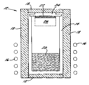
BRIEF DESCRIPTION OF THE DRAWINGS
[0018] Figure 1 is a photograph of a SiC wafer in accordance with the present
invention;
[0019] Figure 2 is a semiconductor precursor wafer in accordance with the
present
invention;
[0020] Figure 3 is a plurality of semiconductor precursor devices in
accordance with
the present invention;
[0021] Figure 4 is a schematic cross-sectional view of a seeded sublimation
system in
accordance with the present invention;
CA 02581856 2009-09-24
-4c-
[00221 Figure 5 is a schematic cross-sectional view of a metal oxide
semiconductor
field effect transistor in accordance with the present invention; and
[00231 Figure 6 is a schematic cross-sectional view of a metal semiconductor
field
effect transistor in accordance with the present invention.
DETAILED DESCRIPTION
[00241 The present invention relates to high quality silicon carbide wafers.
In
particular, the present invention incorporates several techniques for
improving the
growth of such wafers using seeded sublimation.
CA 02581856 2007-03-26
WO 2006/041660 PCT/US2005/034352
-5-
[0025] In one aspect, the present invention is a high quality single crystal
wafer of SiC
having a diameter of at least about 100 mm and a micropipe density less than
about 25
cm2, more preferably less than about 20 cm 2, and most preferably less than
about 10 cm
2. The polytype of the single crystal SiC is preferably 3C, 4H, 6H, 2H, or
15R.
[0026] In considering the proportional dimensions of the diameter and
thickness of
the seed crystal, whether expressed as a percentage, a fraction, or a ratio,
it will be
understood that in the context of the improvements provided by the invention,
these
proportions have their inventive meaning in the context of the larger-diameter
seed
crystals that are described herein.
[0027] Accordingly, in certain embodiments the invention is described and
claimed herein in the relevant embodiments in a manner that includes the
absolute
dimensions of the crystal, usually in terms of a diameter, of which 2 inch, 3
inch, and
100 mm diameter single crystals are preferred.
[0028] Figure 1 is a photograph of a wafer 2 in accordance with the present
invention.
Black spots on the surface are micropipes. When appropriately counted, this
exemplary
wafer has fewer than 25 micropipes per square centimeter.
[0029] In another aspect, the invention is a high quality semiconductor
precursor
wafer. The wafer is a silicon carbide wafer of the 4H polytype, having a
diameter of at
least about 100 mm and a micropipe density on its surface of between about 7
and 22 cm-
2 . The surface micropipe density represents a count of the total micropipes
on the surface
divided by the surface area of the wafer. The count of total micropipes
represents a count
of total micropipes on the surface after an etch that preferentially
emphasizes micropipe
defects. The etch is preferably a molten potassium hydroxide etch. It will be
understood
measurable areas of crystals according to the present invention exhibit
micropipe
densities of less than 22 cm2, in some cases less than 7 CM-2 , and in yet
other cases to
date predictive-none. Thus, as used herein the expression "less than" has both
measured
and predictive aspects. In addition to the measured aspects (e.g., Figure 1),
it is expected
that some crystals will demonstrate even fewer defects. As a result, the
phrase, "less
than" (e.g. "less than 7 CM-2 ) as used herein also includes (but is not
limited to) ranges
such as 7 - 22 cm 2.
[0030] In yet another aspect, the invention is a high quality semiconductor
precursor wafer of silicon carbide having a 4H polytype, a diameter of at
least about 100
CA 02581856 2007-03-26
WO 2006/041660 PCT/US2005/034352
-6-
mm, and between about 545 and 1730 micropipes on the surface of the wafer.
Again, the
surface micropipes represent a count of the total micropipes on the surface,
preferably
after the molten potassium hydroxide etch.
[00311 In another aspect as schematically depicted in Figure 2, the invention
is a
high quality silicon carbide semiconductor precursor wafer 4 having a 4H
polytype, a
diameter of at least about 100 nun, and a micropipe density on its surface of
less than
22 CM-2 . The wafer additionally has a Group III-nitride layer 6 located on
the surface.
The Group III-nitride layer 6 is preferably one or more of GaN, AlGaN, A1N,
AlInGaN,
InN, and AlInN.
[00321 The growth and electronic characteristics of Group III nitrides are
generally well-understood in this art. Group III nitride layers on silicon
carbide
substrates are a basic feature of certain types of light emitting diodes
(LEDs). Among
other desirable factors, the atonic fraction of the Group III element (e.g.
1nnGayN1_X_y)
tailors the bandgap of the composition (within limits) to likewise tailor the
resulting
emission frequency and thus the color of the LED.
[0033] With respect to Figure 3, the invention is a plurality of silicon
carbide
semiconductor device precursors 8 on a SiC seed 9 having a diameter of at
least about
100 mm and a micropipe density on the surface of the wafer of between about 7
and 22
cm2. The wafer additionally has a plurality of respective Group III-nitride
epitaxial
layers 10 on some portions of the wafer. Preferred Group III-nitride epitaxial
layers are
individually selected from GaN, AlGaN, A1N, AlInGaN, InN, and AlInN.
[00341 In another aspect, the invention is a method of producing a high
quality
bulls single crystal of silicon carbide in a seeded sublimation system, the
improvement
includes growing a SiC boule having a diameter of at least about 100 mm and
having a
micropipe density of less than about 20 cm 2, thereafter slicing the SiC
boule, preferably
mechanically, into wafers, wherein each wafer has a micropipe density of less
than about
20 cm 2 on the surface. The wafers are preferably about 0.5 mm thick.
[00351 It may be preferable to then polish and etch the SiC wafers. A
preferred
polish is a chemo-mechanical polish and a preferred etch is a molten KOH etch.
The
etch is carried out in order to highlight the defects on the surface, and is
unnecessary as a
precursor step to seeded sublimation. Thus, sublimation growth is typically
carried out
on a polished seed that has not been etched.
CA 02581856 2007-03-26
WO 2006/041660 PCT/US2005/034352
-7-
[0036] As is known in the art, the SiC boule is preferably grown in a seeded
sublimation system. After the boule is sliced into wafers, the wafers may
then, in turn,
be used as the seed in a seeded sublimation growth of a single crystal of
silicon carbide.
[0037] As noted in the background portion of the specification, the general
aspects
of seeded sublimation growth of silicon carbide have been generally well
established for
a number of years. Furthermore, those familiar with the growth of crystals,
particularly
in difficult material systems such as silicon carbide, will recognize that the
details of a
given technique can and will vary, usually purposefully, depending upon the
relevant
circumstances. Accordingly, the descriptions given herein are most
appropriately given
in a general and schematic sense with the recognition that those persons of
skill in this
art will be able to carry out the improvements of the invention based on the
disclosures
herein without undue experimentation.
[0038] In describing the invention, it will be understood that a number of
techniques are disclosed. Each of these has individual benefit, and each can
also be used
in conjunction with one or more, or in some cases all, of the other disclosed
techniques.
Accordingly, for the sake of clarity, this description will refrain from
repeating every
possible combination of the individual steps in an unnecessary fashion.
Nevertheless,
the specification and claims should be read with the understanding that such
combinations are entirely within the scope of the invention and the claims.
[0039] Figure 4 is a cross sectional schematic diagram of a sublimation system
for
seeded sublimation growth of the type contemplated as useful in the present
invention.
The system is broadly designated at 12. As in most typical systems, the system
12
includes a graphite susceptor, or crucible, 14 and a plurality of induction
coils 16 that
heat the susceptor 14 when current is applied through the coils 16.
Alternatively, some
systems incorporate resistance heating. It will be understood by those
familiar with these
crystal growth techniques that the system can be further enclosed in some
circumstances,
e.g., in a water-cooled quartz vessel. Additionally, at least one gas inlet
and outlet (not
shown) in communication with the susceptor 14 are included in the seeded
sublimation
system 12. Such further enclosures are, however, less relevant to the
invention and are
omitted herein to help clarify the drawing and description. Additionally,
those persons
skilled in this art recognize that silicon carbide sublimation systems of the
type described
herein are available both commercially and as constructed in a custom fashion
as may be
CA 02581856 2007-03-26
WO 2006/041660 PCTIUS2005/034352
-8-
necessary or appropriate. They accordingly can be selected or designed by
those of
ordinary skill in this art without undue experimentation.
[0040] The susceptor 14 is typically surrounded by insulation 18, several
portions
of which are illustrated in Figure 4. Although Figure 4 illustrates the
insulation as being
generally consistent in size and placement, it will be understood and is
recognized by
those of skill in the art that the placement and amount of the insulation 18
can be used to
provide desired thennal gradients (both axially and radially) along the
susceptor 14.
Again, for purposes of simplification, these possible permutations are not
illustrated
herein.
[0041] The susceptor 14 includes one or more portions for containing a silicon
carbide powder source 20. Such a powder source 20 is most commonly-although
not
exclusively-used in seeded sublimation growth techniques for silicon carbide.
Figure 4
illustrates the powder source 20 as being contained in a lower portion of the
susceptor 14
and this is one typical arrangement. As another familiar variation, some
systems
distribute the source powder in a vertical, cylindrical arrangement in which
the source
powder surrounds a larger portion of the interior of the susceptor 14 than
does the
arrangement illustrated in Figure 4. The invention described herein can be
appropriately
carried out using both types of equipment.
[0042] A silicon carbide seed is designated at 22, and is typically placed in
upper
portions of the susceptor 14. The seed 22 is preferably a monocrystalline SiC
seed
having a diameter of at least about 100 mm and having a micropipe density of
less than
about 25 CM -2 on the surface. A growing crystal 26 is deposited on the seed
22 during
the seeded sublimation growth.
[0043] A seed holder 28 typically holds the seed 22 in place with the seed
holder
28 being attached to the susceptor 14 in an appropriate fashion. This can
include various
resting or threaded arrangements. In the orientation illustrated in Figure 4,
the upper
portions of the seed holder 28 would typically include threads as would the
uppermost
portions of the susceptor 14, preferably a graphite crucible, so that the seed
holder 28
could be threaded into the top of the susceptor 14 to hold the seed 22 in the
desired
position. The seed holder 28 is preferably a graphite seed holder.
[0044] It may be preferable to place the seed 22 in the crucible 14 while
exerting
minimal torsional forces on the seed 22 to thereby prevent torsional forces
from warping
CA 02581856 2007-03-26
WO 2006/041660 PCT/US2005/034352
-9-
or bowing the crystal in a manner that would otherwise encourage undesired
thermal
differences across the seed 22.
[0045] In some embodiments it may be desirable to anneal the seed holder 28
prior
to attaching the seed 22. Annealing the seed holder 28 prior to sublimation
growth
prevents the seed holder 28 from undergoing significant distortion during
crystal growth
at SiC sublimation temperatures. Annealing the seed holder 28 also minimizes
or
eliminates temperature differences across the seed 22 that would otherwise
tend to
initiate and propagate defects in a growing crystal. A preferred process for
annealing the
seed holder 28 includes annealing at temperatures at or about 2500 C for at
least about
30 minutes.
[0046] In some embodiments, it may be preferred to include dopant atoms in the
sublimation system 12. Introducing dopant gases to the seeded sublimation
system 12
incorporates dopant atoms in a growing crystal. Dopants are selected for their
acceptor
or donor capabilities. Donor dopants are those with n-type conductivity and
acceptor
dopants are those with p-type conductivity. Preferred dopant atoms include n-
type and
p-type dopant atoms. Especially preferred n-type dopants include N, P, As, Sb,
Bi, and
mixtures thereof. Especially preferred p-type dopants include B, Al, Ga, In,
Ti, and
mixtures thereof.
[0047] The general scheme for sublimation growth is set forth briefly in the
Background portion of the specification, as well as in other sources well-
known to those
of ordinary skill in this art. Typically, an electric current, having a
frequency to which
the susceptor 14 responds, is passed through the induction coils 16 to heat
the graphite
susceptor 14. The amount and placement of the insulation 18 are selected to
create a
thermal gradient between the powder source 20 and the growing crystal 26 when
the
susceptor 14 heats the powder source 20 to sublimation temperatures, which are
typically
above about 2000 C. The thermal gradient is established to maintain the
temperature of
the seed 22 and thereafter a growing crystal near, but below, the temperature
of the
silicon carbide source to thereby thermodynamically encourage the vaporized
species
that are generated when silicon carbide sublimes (Si, Si2C, and SiC2) to
condense first
upon the seed crystal and thereafter upon the growing crystal; e.g., U.S.
Patent No.
4,866,005.
CA 02581856 2007-03-26
WO 2006/041660 PCT/US2005/034352
-10-
[0048] After reaching the desired crystal size, growth is terminated by
reducing the
temperature of the system to below about 1900 C and raising the pressure to
above
about 400 torr.
[0049] It may be further desirable to anneal the crystal after completion of
the
sublimation growth process. The crystal may be annealed at temperatures at or
above the
growth temperature for a period greater than about 30 minutes.
[0050] For purposes of clarity, the singular term, "thermal gradient," will be
used
herein, but it will be understood by those of skill in this art that several
gradients can
desirably co-exist in the susceptor 14 and can be subcategorized as axial and
radial
gradients, or as a plurality of isotherms.
[0051] If the temperature gradients and other conditions (pressure, carrier
gases,
etc.) are properly maintained, the overall thermodynamics will encourage the
vaporized
species to condense first on the seed 22 and then on the growing crystal 26 in
the same
polytype as the seed 22.
[0052] As generally noted in the Background, the performance properties of
electronic devices will typically improve as the crystal quality of the
various device
portions improves. Thus, the reduced-defect characteristics of wafers of the
present
invention similarly provide improved devices. In particular, higher power
higher current
devices become increasingly available as the micropipe density drops to 20 cm -
2 or
below.
[0053] Thus, in another aspect, the invention is a plurality of field-effect
transistors
formed on low-defect 100 mm silicon carbide wafers. Each field-effect
transistor
includes a bulk single crystal silicon carbide substrate wafer of at least
about 100 mm
diameter and having a micropipe density of between about 7 and 22 cm2.
[0054] In another aspect, the invention is a plurality of metal oxide
semiconductor
field effect transistors (MOSFETs) 42 formed on low defect 100 mm silicon
carbide
substrate 44. Figure 5 is a schematic cross-sectional illustration of a basic
MOSFET
structure. Each MOSFET 42 includes a bulk single crystal silicon carbide
substrate
wafer 44 of at least about 100 mm diameter and a micropipe density of less
than 22 em 2,
in some cases between about 7 and 22 CM-2 , and in some cases-to date
predictive-less
than 7 cm2. The bulk single crystal substrate 44 includes a respective first
surface 48
and second surface 50 opposite one another. An epitaxial layer on the
substrate has
CA 02581856 2007-03-26
WO 2006/041660 PCT/US2005/034352
-11-
respective source 52, channel 56, and drain 54 portions with the channel 56
being
controlled by the gate contact 64 through the oxide layer 62. Respective
source and
drain contacts 58, 60 are on the source and drain portions 52, 54. The
structure and
operation of MOSFETs, and of combinations and variations of MOSFETs, is well
understood in this art and thus Figure 5 and its description are exemplary
rather than
limiting of the claimed invention.
[0055] With reference to Figure 6, in another aspect the invention is a
plurality of
metal semiconductor field effect transistors (MESFETs) 66 formed on low defect
100
mm silicon carbide. Each MESFET 66 includes a bulk single crystal silicon
carbide
substrate wafer 68 of at least about 100 mm and having a micropipe density of
between
about 7 and 22 cm 2. The substrate 68 includes a respective first surface 70
and second
surface 72 opposite one another. A conductive channel 74 is located on the
first surface
70 of the substrate 68. Ohmic source 76 and a drain 78 contacts are located on
the
conductive channel 74. A metal gate contact 80 is located between the source
76 and
drain 78 on the conductive channel 74 for forming an active channel when a
bias is
applied to the metal gate contact 80.
[0056] As is known in the art, more than one type of device may be situated on
a
silicon carbide wafer in accordance with the present invention. Additional
devices that
may be included are junction-field effect transistors, hetero field effect
transistors,
diodes, and other devices known in the art. The structure and operation of
these (and
other) devices are well-understood in this art and can be practiced using the
substrates
described and claimed herein without undue experimentation.
EXAMPLES
[0057] A series of SiC boules were formed according to the present invention.
The micropipe density, as measured by the above-described counting method, of
each of
these boules is shown in Table 1.
Table 1: Micropipe Density of SiC boules
Boule Number Micropipe Density (cm-:)_
1 21.82
2 20.21
3 19.97
4 18.42
CA 02581856 2007-03-26
WO 2006/041660 PCT/US2005/034352
-12-
16.67
6 15.96
7 15.61
8 7.23
[0058] In the specification and the drawings, typical embodiments of the
invention
have been disclosed. Specific terms have been used only in a generic and
descriptive
sense, and not for purposes of limitation. The scope of the invention is set
forth in the
following claims.