Note : Les descriptions sont présentées dans la langue officielle dans laquelle elles ont été soumises.
CA 02588114 2007-05-11
WO 2006/057686 PCT/US2005/031272
Attorney Docket No. 5308-373
CAP LAYERS AND/OR PASSIVATION LAYERS FOR NITRIDE-BASED
TRANSISTORS, TRANSISTOR STRUCTURES AND METHODS OF
FABRICATING SAME
FIELD OF THE INVENTION
The present invention relates to semiconductor devices and, more particularly,
to transistors that incorporate nitride-based'active layers.
BACKGROUND
Materials such as silicon (Si) and-gallium arsenide (GaAs) have found wide
application in semiconductor devices for lower power and (in the case of Si)
lower
frequency applications. These, more familiar, semiconductor materials may not
be
well suited for higher power and/or high frequency applications, however,
because of
their relatively small bandgaps (e.g., 1.12 eV for Si and 1.42 for GaAs at
room
temperature) and/or relatively small breakdown voltages.
In light of the difficulties presented by Si and GaAs, interest in high power,
high temperature and/or high frequency applications and devices has turned to
wide
bandgap semiconductor materials such as silicon carbide (2.996 eV for alpha
SiC at
room temperature) and the Group III nitrides (e.g., 3.36 eV for GaN at room
temperature). These materials, typically, have higher electric field breakdown
strengths and higher electron saturation velocities as compared to gallium
arsenide
and silicon.
A device of particular interest for high power and/or high frequency
applications is the High Electron Mobility Transistor (HEMT), which, in
certain
cases, is also known as a modulation doped field effect transistor (MODFET).
These
devices may offer operational advantages under a number of circumstances
because a
two-dimensional electron gas (2DEG) is formed at the heterojunction of two
semiconductor materials with different bandgap energies, and where the smaller
bandgap material has a higher electron affinity. The 2DEG is an accumulation
layer in
the undoped ("unintentionally doped"), smaller bandgap material and can
contain a
very high sheet electron concentration in excess of, for example, 1013
carriers/cm2.
Additionally, electrons that originate in the wider-bandgap semiconductor
transfer to
1
CA 02588114 2007-05-11
WO 2006/057686 PCT/US2005/031272
the 2DEG, allowing a high electron mobility due to reduced ionized impurity
scattering.
This combination of high carrier concentration and high carrier mobility can
give the HEMT a very large transconductance and may provide a strong
performance
advantage over metal-semiconductor field effect transistors (MESFETs) for high-
frequency applications.
High electron mobility transistors fabricated in the gallium nitride/aluminum
gallium nitride (GaN/AlGaN) material system have the potential to
generate.large
amounts of RF power because of the combination of material characteristics
that
includes the aforementioned high breakdown fields, their wide bandgaps, large
conduction band offset, and/or high saturated electron drift velocity. A major
portion
of the electrons in the 2DEG is attributed to polarization in the AlGaN.
HEMTs in the GaN/AlGaN system have already been demonstrated. U.S. Patents
5,192,987 and 5,296,395 describe AlGaN/GaN HEMT structures and methods of
manufacture. U.S. Patent No. 6,316,793, to Sheppard et al., which is commonly
assigned and is incorporated herein by reference, describes a HEMT device
having a
semi-insulating silicon carbide substrate, an aluminum nitride buffer layer on
the
substrate, an insulating gallium nitride layer on the buffer layer, an
aluminum gallium
nitride barrier layer on the gallium nitride layer, and a passivation layer on
the
aluminum gallium nitride active structure.
SUMMARY OF THE INVENTION
Some embodiments of the present invention provide Group I1I-nitride high
electron mobility transistors and methods of fabricating Group III-nitride
high
electron mobility transistors that include a Group III-nitride based channel
layer, a
Group I1I-nitride based barrier layer on the channel layer and a non-uniform
composition AlGaN based cap layer on the barrier layer. The non-uniform
composition AlGaN based cap layer has a higher concentration of Al adjacent a
surface of the cap layer that is remote from the barrier layer than is present
in a region
within the AlGaN based cap layer. In particular embodiments of the present
invention
having a gate recessed through the cap layer, the higher concentration of Al
extends
into the cap layer from about 30 A to about 1000 A. In particular embodiments
of the
present invention having a gate on the cap layer, the higher concentration of
Al
extends into the cap layer from about 2.5 A to about 100 A.
2
CA 02588114 2007-05-11
WO 2006/057686 PCT/US2005/031272
In further embodiments of the present invention, the AlGaN based cap layer
includes a first region of AlXGal_XN at the surface of the cap layer, where
x<1 and a
second region of AlyGal_y N within the AIGaN based cap layer, where y<l and
y<x.
The value of x may be from about 0.2 to about 1 and y is from about 0.15 to
about
0.3. In particular embodiments of the present invention, the difference
between x and
y and/or the thickness of the cap layer may be selected to prevent formation
of a
second 2DEG in the cap layer. In other embodiments of the present invention
where
the gate is recessed through the cap layer but does not touch the cap layer,
the
difference between x and y and/or the thiclcness of the cap layer may be
selected to
provide a second 2DEG in the cap layer.
In additional embodiments of the present invention, the AlGaN based cap
layer further includes a third region of A1,Gai_,N at an interface between the
barrier
layer and the AlGaN based cap layer, where z<1 and z#y. In some embodiments,
z>
y. In other embodiments, z> x. In still ftirther embodiments, z< x.
In particular embodiments of the present invention, the channel layer
comprises a GaN layer, the barrier layer comprises an AIGaN layer and the cap
layer
comprises an AIGaN layer.
Some embodiments of the present invention provide Group III-nitride high
electron mobility transistors and methods of fabricating Group 111-nitride
high
electron mobility transistors that include a Group III-nitride based channel
layer, a
Group 111-nitride based barrier layer on the channel layer and a GaN based cap
layer
on the barrier layer. The GaN based cap layer has a doped region adjacent a
surface
of the cap layer and is remote from the barrier layer.
In certain embodiments, the doped region is a region doped with n-type
dopants. In particular embodiments of the present invention without a gate
recess, the
doped region extends into the cap layer from about 2.5 A to about 50 A. In
particular
embodiments of the present invention with a gate recess, the doped region
extends
into the cap layer from about 20 A to about 5000 A. The doped region may
provide a
dopant concentration of from about 10 18 to about 1021 cm 3. The n-type
dopants may
be Si, Ge or O. In particular embodiments of the present invention, the doped
region
may be one or more delta-doped regions at or near the surface of the cap layer
and
may, for example, have a dopant concentration of from about 10 " to about 1015
em-2.
In particular embodiments of the present invention, the dopant is 0 that
extends into
the cap layer about 20 A.
3
CA 02588114 2007-05-11
WO 2006/057686 PCT/US2005/031272
In other embodiments, the doped region is a region doped with p-type dopants.
In particular embodiments of the present invention without a gate recess, the
doped
region extends into the cap layer from about 2.5 A to about 50 A. In
particular
embodiments of the present invention with a gate recess, the doped region
extends
into the cap layer from about 30 A to about 5000 A. The doped region may
provide a
dopant concentration of from about 1016 to about 1022 cm 3. The p-type dopants
may
be Mg, Be, Zn, Ca or C. In particular embodiments of the present invention,
the
doped region may be one or more delta-doped regions at or near the surface of
the cap
layer and may, for example, have a dopant concentration of from about 10~ ~ to
about
1015 cm-2.
In still further embodiments, the doped region is a region doped with deep
level dopants. In particular embodiments of the present invention without a
gate
recess, the doped region extends into the cap layer from about 2.5 A to about
100 A.
In particular embodiments of the present invention with a gate recess, the
doped
region extends into the cap layer from about 30 A to about 5000 A. The doped
region
may provide a dopant concentration of from about 1016 to about 1022 cm"3. The
deep
level dopants may be Fe, C, V, Cr, Mn, Ni, Co or other rare earth elements.
In additional embodiments of the present invention, the doped region is a
first
doped region and the cap layer further includes a second doped region. The
second
doped region has a dopant concentration less than the dopant concentration of
the first
doped region. The second doped region may be the remainder of the cap layer
not in
the first doped region.
In particular embodiments, the channel layer comprises a GaN layer, the
barrier layer comprises an AlGaN layer and the cap layer comprises a GaN or an
AlGaN layer.
Some embodiments of the present invention, provide methods for passivating
a surface of a wide bandgap semiconductor device that include forming a
graphitic
and/or amorphous BN layer on a least a portion of a surface of a region of
wide
bandgap semiconductor material of the wide-bandgap semiconductor device.
Corresponding structures are also provided.
In further embodiments of the present invention, the wide bandgap
semiconductor device is a Group III-nitride semiconductor device. For example,
the
wide bandgap semiconductor device may be a GaN based semiconductor device.
4
CA 02588114 2007-05-11
WO 2006/057686 PCT/US2005/031272
Furthermore, the wide bandgap semiconductor device may be a Group 111-nitride
high
electron mobility transistor.
In additional embodiments of the present invention, forming the graphitic
and/or amorphous BN layer is carried out at a temperature less than a
decomposition
temperature of wide bandgap semiconductor materials in the wide bandgap
semiconductor device. Forming the graphitic and/or amorphous BN layer may be
carried out at a temperature less than about 1100 C, in some embodiments at a
temperature of less than about 1000 C and in particular embodiments at a
temperature of less than about 900 C. Also, the BN layer may formed to be non-
single crystal. The graphitic and/or amorphous BN layer may be formed to a
thickness of from about 3 A to about 1 m.
Some embodiments of the present invention provide methods of passivating a
surface of a Group 111-nitride semiconductor device by forming a SiC layer on
a least
a portion of a surface of a region of Group III-nitride semiconductor material
of the
Group III-nitride semiconductor device. Corresponding structures are also
provided.
In certain embodiments, the Group 111-nitride semiconductor device may be a
GaN based semiconductor device. In further embodiments, the Group 111-nitride
semiconductor device may be a Group 111-nitride high electron mobility
transistor.
In additional embodiments of the present invention, forming the SiC layer is
carried out at a temperature less than a decomposition temperature of Group
III-
nitride semiconductor materials in the Group 111-nitride semiconductor device.
For
example, forming the SiC layer is carried out at a temperature less than about
1100
C, in some embodiments at a temperature of less than about 1000 C and in
particular embodiments at a temperature of less than about 900 C. Also, the
SiC
layer may be formed to be non-single crystal. In particular embodiments,
forming the
SiC layer comprises forming a 3C SiC layer. The SiC layer may be formed to a
thickness of from about 3 A to about 1 m.
Further embodiments of the present invention comprise methods of providing
passivation structures for wide bandgap semiconductor devices, such as Group
III-
nitride semiconductor devices, comprising annealing a passivation layer
directly on a
Group III-nitride layer in an oxygen containing environment. The passivation
layer
may be, for example, SiN, BN, MgN and/or SiC. In still other embodiments, the
passivation layer includes Si02, MgO, A1203, Sc203 and/or A1N.
5
CA 02588114 2007-05-11
WO 2006/057686 PCT/US2005/031272
The annealing may be carried out at a temperature of from about 100 C to
about 1000 C and for a time of from about 10 seconds to about 1 hour. The
oxygen
containing environment may be only oxygen, oxygen in N2, oxygen in another
inert
gas, such as argon, oxygen in dry air, CO, C02, NO, NO2 and/or ozone. The
annealing may be performed at a temperature and for a time insufficient to
oxidize the
structure underlying the passivation layer but sufficient to remove at least
some
hydrogen from the passivation layer. Some carbon may also be removed from the
passivation layer.
Additional embodiments of the present invention provide methods of
fabricating a passivation structure for a Group III-nitride semiconductor
device by
forming a passivation layer directly on a least a portion of a surface of a
region of
Group III-nitride semiconductor material of the Group III-nitride
semiconductor
device and annealing the passivation layer in D2 and/or D20. In some
embodiments,
the passivation layer includes SiN and/or MgN. In other embodiments, the
passivation layer includes BN and/or SiC. In still other embodiments, the
passivation
layer includes Si02, MgO, A1203, Sc203 and/or A1N.
The annealing may be performed at a temperature and for a time insufficient
to oxidize a structure underlying the passivation layer but sufficient to
remove at least
some hydrogen from the passivation layer or exchange some hydrogen with
deuterium. Furthermore, the Group III-nitride semiconductor material may be a
GaN
based material.
Additional embodiments of the present invention provide Group III-nitride
high electron mobility transistors and method of fabricating Group III-nitride
high
electron mobility transistors that include a Group III-nitride based channel
layer, a
Group III-nitride based barrier layer on the channel layer and an A1N cap
layer on the
barrier layer. The transistor may further include a gate contact recessed into
the A1N
cap layer. In such embodiments, the A1N cap layer has a thickness of from
about 5 to
about 5000 A. In some embodiments of the present invention, the A1N layer may
not
be coherent with the underlying layer, may be non-single crystalline, may be
formed
ex-situ and/or may be formed by a lower quality formation process, such as by
PVD
rather than CVD. The transistor may also include a gate contact on the AIN cap
layer
and not recessed into the A1N cap layer. In such embodiments, the A1N cap
layer has
a thickness of from about 2 A to about 20 A. Additionally, the channel layer
may be a
GaN layer and the barrier layer may be an AlGaN layer.
6
CA 02588114 2007-05-11
WO 2006/057686 PCT/US2005/031272
Still further embodiments of the present invention provide Group III-nitride
high electron mobility transistors and methods of fabricating Group III-
nitride high
electron mobility transistors that include a Group III-nitride based channel
layer, a
Group 111-nitride based barrier layer on the channel layer, a protective layer
on the
barrier layer, a gate contact on the barrier layer and ohmic contacts on the
protective
layer. In some embodiments of the present invention, the protective layer
includes
SiN. In other embodiments, the protective layer includes BN or MgN. In further
embodiments, the protective layer comprises multiple layers, such as a layer
of SiN
and a layer of A1N. In particular embodiments of the present invention, the
protective
layer has a thickness of from about 1 A to about 10. A. In certain
embodiments, the
protective layer has a thickness of about one monolayer.
In still further embodiments of the present invention, the gate contact is on
the
protective layer. Also, the ohmic contacts may be directly on the protective
layer.
The protective layer may be formed in-situ with forming the barrier layer.
Various combinations and/or sub-combinations of cap layers, passivation
layers, protective layers and/or anneals of passivation layers may also be
provided
according to some embodiments of the present invention.
BRIEF DESCRIPTION OF THE DRAWINGS
Figures 1A and 1B are cross-sectional schematic drawings illustrating
transistors having a cap layer according to some embodiments of the present
invention.
Figures 2A and 2B are cross-sectional schematic drawings illustrating
transistors having a cap layer according to some embodiments of the present
invention.
Figure 3A and 3B are cross-sectional schematic drawings illustrating
graphitic and/or amorphous BN passivation layers according to some embodiments
of
the present invention.
Figure 4A and 4B are cross-sectional schematic drawings illustrating SiC
passivation layers according to some embodiments of the present invention.
Figures 5A and 5B are cross-sectional schematic drawings illustrating
transistors having a cap layer according to some embodiments of the present
invention.
7
CA 02588114 2007-05-11
WO 2006/057686 PCT/US2005/031272
Figure 6 is a cross-sectional schematic drawing illustrating transistors
having
ohmic contacts on a protective layer according to some embodiments of the
present
invention.
DETAILED DESCRIPTION OF EMBODIMENTS OF THE INVENTION
The present invention now will be described more fully hereinafter with
reference to the accompanying drawings, in which embodiments of the invention
are
shown. However, this invention should not be construed as limited to the
embodiments set forth herein. Rather, these embodiments are provided so that
this
disclosure will be thorough and complete, and will fully convey the scope of
the
invention to those skilled in the art. In the drawings, the thickness of
layers and
regions are exaggerated for clarity. Like numbers refer to like elements
throughout.
As used herein the term "and/or" includes any and all combinations of one or
more of
the associated listed items.
The terminology used herein is for the purpose of describing particular
embodiments only and is not intended to be limiting of the invention. As used
herein,
the singular forms "a", "an" and "the" are intended to include the plural
forms as well,
unless the context clearly indicates otherwise. It will be further understood
that the
terms "comprises" and/or "comprising," when used in this specification,
specify the
presence of stated features, integers, steps, operations, elements, and/or
components,
but do not preclude the presence or addition of one or more other features,
integers,
steps, operations, elements, components, and/or groups thereof.
It will be understood that when an element such as a layer, region or
substrate
is referred to as being "on" or extending "onto" another element, it can be
directly on
or extend directly onto the other element or intervening elements may also be
present.
In contrast, when an element is referred to as being "directly on" or
extending
"directly onto" another element, there are no intervening elements present. It
will also
be understood that when an element is referred to as being "connected" or
"coupled"
to another element, it can be directly connected or coupled to the other
element or
intervening elements may be present. In contrast, when an element is referred
to as
being "directly connected" or "directly coupled" to another element, there are
no
intervening elements present. Like numbers refer to like elements throughout
the
specification.
8
CA 02588114 2007-05-11
WO 2006/057686 PCT/US2005/031272
It will be understood that, although the terms first, second, etc. may be used
herein to describe various elements, components, regions, layers and/or
sections, these
elements, components, regions, layers and/or sections should not be limited by
these
terms. These terms are only used to distinguish one element, component,
region,
layer or section from another region, layer or section. Thus, a first element,
component, region, layer or section discussed below could be termed a second
element, component, region, layer or section without departing from the
teachings of
the present invention.
Furthermore, relative terms, such as "lower" or "bottom" and "upper" or "top,"
may be used herein to describe one element's relationship to another elements
as
illustrated in the Figures. It will be understood that relative terms are
intended to
encompass different orientations of the device in addition to the orientation
depicted
in the Figures. For example, if the device in the Figures is turned over,
elements
described as being on the "lower" side of other elements would then be
oriented on
"upper" sides of the other elements. The exemplary term "lower", can
therefore,
encompass both an orientation of "lower" and "upper," depending of the
particular
orientation of the figure. Similarly, if the device in one of the figures is
turned over,
elements described as "below" or "beneath" other elements would then be
oriented
"above" the other elements. The exemplary terms "below" or "beneath" can,
therefore,
encompass both an orientation of above and below. Furthermore, the term
"outer"
may be used to refer to a surface and/or layer that is farthest away from a
substrate.
Embodiments of the present invention are described herein with reference to
cross-section illustrations that are schematic illustrations of idealized
embodiments of
the present invention. As such, variations from the shapes of the
illustrations as a
result, for example, of manufacturing techniques and/or tolerances, are to be
expected.
Thus, embodiments of the present invention should not be construed as limited
to the
particular shapes of regions illustrated herein but are to include deviations
in shapes
that result, for example, from manufacturing. For example, an etched region
illustrated as a rectangle will, typically, have tapered, rounded or curved
features.
Thus, the regions illustrated in the figures are schematic in nature and their
shapes are
not intended to illustrate the precise shape of a region of a device and are
not intended
to limit the scope of the present invention.
Unless otherwise defined, all terms (including technical and scientific terms)
used herein have the same meaning as commonly understood by one of ordinary
skill
9
CA 02588114 2007-05-11
WO 2006/057686 PCT/US2005/031272
in the art to which this invention belongs. It will be further understood that
terms,
such as those defined in commonly used dictionaries, should be interpreted as
having
a meaning that is consistent with their meaning in the context of the relevant
art and
will not be interpreted in an idealized or overly formal sense unless
expressly so
defined herein.
It will also be appreciated by those of skill in the art that references to a
structure or feature that is disposed "adjacent" another feature may have
portions that
overlap or underlie the adjacent feature.
Embodiments of the present invention may be particularly well suited for use
in nitride-based devices such as Group III-nitride based HEMTs. As used
herein, the
term "Group III nitride" refers to those semiconducting compounds formed
between
nitrogen and the elements in Group III of the periodic table, usually aluminum
(Al),
gallium (Ga), and/or indium (In). The term also refers to ternary and
quaternary
compounds such as AIGaN and AlInGaN. As is well understood by those in this
art,
the Group III elements can combine with nitrogen to form binary (e.g., GaN),
ternary
(e.g., AIGaN, AIInN), and quaternary (e.g., AIInGaN) compounds. These
compounds
all have empirical formulas in which one mole of nitrogen is combined with a
total of
one mole of the Group III elements. Accordingly, formulas such as AIGat_XN
where
0<_ x<_ 1 are often used to describe them.
Suitable structures and techniques for fabricating GaN-based HEMTs that may
utilize embodiments of the present invention are described, for example, in
commonly
assigned U.S. Patent 6,316,793 and U.S. Patent Publication No. 2002/0066908A1
filed July 12, 2001 and published June 6, 2002, for "ALUMINUM GALLIUM
NITRIDE/GALLIUM NITRIDE HIGH ELECTRON MOBILITY TRANSISTORS
HAVING A GATE CONTACT ON A GALLIUM NITRIDE BASED CAP
SEGMENT AND METHODS OF FABRICATING SAME," U. S. Patent Publication
No. 2002/0167023A1 to Smorchkova et al., published November 14, 2002, entitled
"GROUP-III NITRIDE BASED HIGH ELECTRON MOBILITY TRANSISTOR
(HEMT) WITH BARRIER/SPACER LAYER", U.S. Patent Application Serial No.
10/617,843 filed July 11, 2003 for "NITRIDE-BASED TRANSISTORS AND
METHODS OF FABRICATION THEREOF USING NON-ETCHED CONTACT
RECESSES," U.S. Patent Application Serial No. 10/772,882 filed February 5,
2004
for "NITRIDE HETEROJUNCTION TRANSISTORS HAVING CHARGE-
CA 02588114 2007-05-11
WO 2006/057686 PCT/US2005/031272
TRANSFER INDUCED ENERGY BARRIERS AND METHODS OF
FABRICATING THE SAME," U.S. Patent Application Serial No. Serial No.:
10/897,726, filed July 23, 2004 entitled "METHODS OF FABRICATING NITRIDE-
BASED TRANSISTORS WITH A CAP LAYER AND A RECESSED GATE," U.S.
Patent Application Serial No. 10/849,617, filed May 20, 2004 entitled "METHODS
OF FABRICATING NITRIDE-BASED TRANSISTORS HAVING REGROWN
OHMIC CONTACT REGIONS AND NITRIDE-BASED TRANSISTORS HAVING
REGROWN OHMIC CONTACT REGIONS," U.S. Patent Application Serial No.
10/849,589, filed May 20, 2004 and entitled "SEMICONDUCTOR DEVICES HAVING
A HYBRID CHANNEL LAYER, CURRENT APERTURE TRANSISTORS AND
METHODS OF FABRICATING SAME" and U.S. Patent Publication No.
2003/0020092 filed July 23, 2002 and published January 30, 2003 for
"INSULATING
GATE ALGAN/GAN HEMT", the disclosures of which are hereby incorporated
herein by reference in their entirety.
Some embodiments of the present invention provide nitride-based HEMTs
with an AlGaN cap layer that has a higher concentration of AlGaN such as at a
surface that is remote from the barrier layer than at other regions of the
AlGaN cap
layer. Thus, the device may have a layer with a high concentration of Al as an
outer
surface of the device. Such a layer may improve robustness of the device
during
processing and/or device operation over a conventional device that includes a
uniform
Al concentration or a reduced Al concentration at its outer surface. For
example, the
increased Al concentration at the surface may not be susceptible to etching or
other
chemical reactions at high temperatures due to the stronger Al-N bonds
compared to
Ga-N bonds.
In particular embodiments of the present invention, nitride-based HEMTs with
an A1N cap layer on the barrier layer is provided. Thus, the device may have a
layer
with a high concentration of Al as an outer surface of the device that, as
discussed
above, may improve robustness of the device during processing and/or device
operation over a conventional device.
In further embodiments of the present invention, the outer surface of the cap
layer of a nitride-based HEMT is doped with p-type, n-type or deep-level
dopants
such that the cap layer has a higher concentration of dopants at a surface of
the cap
layer that is remote from the barrier layer than at other regions of the cap
layer. The
cap layer may be a GaN based cap layer. The dopants at the outer surface of
the
11
CA 02588114 2007-05-11
WO 2006/057686 PCT/US2005/031272
device may segregate to dislocations in the cap layer and, thereby, reduce
gate
leakage along the dislocations. The dopant may have different characteristics
when at
a dislocation than when in the bulk crystal. For example, a shallow dopant in
the bulk
crystal may have characteristics of a deep level when at a dislocation. Thus,
references to p-type, n-type of deep-level dopants refers to the
characteristics of the
dopants in the bulk crystal rather than at a dislocation. This may be
especially true in
the case of p-type or deep level dopants.
Further embodiments of the present invention provide a graphitic and/or
amorphous BN passivation layer for wide bandgap semiconductor devices. As used
herein, wide bandgap semiconductor devices refers to devices that include a
semiconductor material having a bandgap of greater than about 2.5 eV.
Graphitic
and/or amorphous BN may be particularly well suited for use in GaN based
devices
because B is isovalent with Al, Ga and In and N is present in both materials.
Thus,
neither B nor N are dopants in GaN based structures. In contrast, Si is a
dopant in
GaN. Thus, the formation of a graphitic and/or amorphous BN passivation layer
may
reduce the likelihood of unintended doping of a GaN layer from Si migration.
Furthermore, the graphitic and/or amorphous BN passivation layer may have
reduced
trap levels, different trap energies, different etch selectivity and/or
improved
annealing behavior as compared to conventional passivation materials, such as
SiN or
SiOX.
Further embodiments of the present invention provide a SiC passivation layer
for Group 111-nitride devices. The SiC passivation layer may have reduced trap
levels, different trap energies, different etch selectivity and/or improved
annealing
behavior as compared to conventional passivation materials, such as SiN or
SiOX.
References to SiN, SiON, SiOx, MgN and the like refer to stoichiometric and/or
non-
stoichiometric materials.
Exemplary devices according to some embodiments of the present invention
are schematically illustrated in Figures 1A through 6. Thus, while embodiments
of
the present invention are described herein with reference to a recessed gate
structure
or a non-recessed gate structure, other embodiments of the present invention
may
include or not include a gate recess. Accordingly, embodiments of the present
invention should not be construed as limited to the particular exemplary
embodiments
described herein but may include any suitable structure having a cap layer
and/or
passivation layer as described herein.
12
CA 02588114 2007-05-11
WO 2006/057686 PCT/US2005/031272
Turning to Figures 1A and 1B, a substrate 10 is provided on which nitride
based devices may be formed. In particular embodiments of the present
invention, the
substrate 10 may be a semi-insulating silicon carbide (SiC) substrate that may
be, for
example, 4H polytype of silicon carbide. Other silicon carbide candidate
polytypes
include the 3C, 6H, and 15R polytypes. The term "semi-insulating" is used
descriptively rather than in an absolute sense. In particular embodiments of
the
present invention, the silicon carbide bulk crystal has a resistivity equal to
or higher
than about l x 105 S2-cm at room temperature.
Optional buffer, nucleation and/or transition layers (not shown) may be
provided on the substrate 10. For example, an A1N buffer layer may be provided
to
provide an appropriate crystal structure transition between the silicon
carbide
substrate and the remainder of the device. Additionally, strain balancing
transition
layer(s) may also be provided as described, for example, in commonly assigned
U.S.
Patent Publication No. 2003/0102482A1, filed July 19, 2002 and published June
5,
2003, and entitled "STRAIN BALANCED NITRIDE HETROJUNCTION
TRANSISTORS AND METHODS OF FABRICATING STRAIN BALANCED
NITRIDE HETEROJUNCTION TRANSISTORS," or United States Patent
Publication No. 2004/0012015 Al, filed July 19, 2002 and published January 22,
2004, and entitled "STRAIN COMPENSATED SEMICONDUCTOR STRUCTURES
AND METHODS OF FABRICATING STRAIN COMPENSATED
SEMICONDUCTOR STRUCTURES," the disclosures of which are incorporated
herein by reference as if set forth fully herein.
Appropriate SiC substrates are manufactured by, for example, Cree, Inc., of
Durham, N.C., the assignee of the present invention, and methods for producing
are
described, for example, in U. S. Patent Nos. Re. 34,861; 4,946,547; 5,200,022;
and
6,218,680, the contents of which are incorporated herein by reference in their
entirety.
Similarly, techniques for epitaxial growth of Group III nitrides have been
described
in, for example, U. S. Patent Nos. 5,210,051; 5,393,993; 5,523,589; and
5,592,501,
the contents of which are also incorporated herein by reference in their
entirety.
Although silicon carbide may be used as a substrate material, embodiments of
the present invention may utilize any suitable substrate, such as sapphire,
aluminum
nitride, aluminum gallium nitride, gallium nitride, silicon, GaAs, LGO, ZnO,
LAO,
InP and the like. In some embodiments, an appropriate buffer layer also may be
formed.
13
CA 02588114 2007-05-11
WO 2006/057686 PCT/US2005/031272
Returning to Figures lA and 1B, a channel layer 20 is provided on the
substrate 10. The channel layer 20 may be deposited on the substrate 10 using
buffer
layers, transition layers, and/or nucleation layers as described above. The
channel
layer 20 may be under compressive strain. Furthermore, the channel layer
and/or
buffer nucleation and/or transition layers may be deposited by MOCVD or by
other
techniques known to those of skill in the art, such as MBE or HVPE .
In some embodiments of the present invention, the channel layer 20 is a Group
III-nitride, such as AlGaI _,N where 0<_ x < 1, provided that the energy of
the
conduction band edge of the channel layer 20 is less than the energy of the
conduction
band edge of the barrier layer 22 at the interface between the channel and
barrier
layers. In certain embodiments of the present invention, x = 0, indicating
that the
channel layer 20 is GaN. The channel layer 20 may also be other Group III-
nitrides
such as InGaN, AlInGaN or the like. The channel layer 20 may be undoped
("unintentionally doped") and may be grown to a thickness of greater than
about 20 A.
The channel layer 20 may also be a multi-layer structure, such as a
superlattice or
combinations of GaN, AlGaN or the like.
A barrier layer 22 is provided on the channel layer 20. The channel layer 20
may have a bandgap that is less than the bandgap of the barrier layer 22 and
the
channel layer 20 may also have a larger electron affinity than the barrier
layer 22.
The barrier layer 22 may be deposited on the channel layer 20. In certain
embodiments of the present invention, the barrier layer 22 is A1N, AlInN,
AlGaN or
AlInGaN with a thickness of between about 0.1 nm and about 40 nm. Examples of
layers according to certain embodiments of the present invention are described
in U.S.
Patent Publication No. 2002/0167023A1, to Smorchkova et al., entitled "GROUP-
III
NITRIDE BASED HIGH ELECTRON MOBILITY TRANSISTOR (HEMT) WITH
BARRIER/SPACER LAYER" the disclosure of which is incorporated herein by
reference as if set forth fully herein. In particular embodiments of the
present
invention, the barrier layer 22 is thick enough and has a high enough Al
composition
and doping to induce a significant carrier concentration at the interface
between the
channel layer 20 and the barrier layer 22 through polarization effects. Also,
the
barrier layer 22 should be thick enough to reduce or minimize scattering of
electrons
in the channel due to ionized impurities or imperfections deposited at the
interface
between the barrier layer 22 and the cap layer 24.
14
CA 02588114 2007-05-11
WO 2006/057686 PCT/US2005/031272
The barrier layer 22 may be a Group III-nitride and has a bandgap larger than
that of the channel layer 20 and a smaller electron affinity than the channel
layer 20.
Accordingly, in certain embodiments of the present invention, the barrier
layer 22 is
AlGaN, AlInGaN and/or A1N or combinations of layers thereof. The barrier layer
22
may, for example, be from about 0.1 nm to about 40 nm thick, but is not so
thick as to
cause cracking or substantial defect formation therein. In certain embodiments
of the
present invention, the barrier layer 22 is undoped or doped with an n-type
dopant to a
concentration less than about 1019 cm"3. In some embodiments of the present
invention, the barrier layer 22 is A1XGal_XN where 0< x< 1. In particular
embodiments, the aluminum concentration is about 25%. However, in other
embodiments of the present invention, the barrier layer 22 comprises AlGaN
with an
aluminum concentration of between about 5% and about 100%. In specific
embodiments of the present invention, the aluminum concentration is greater
than
about 10%.
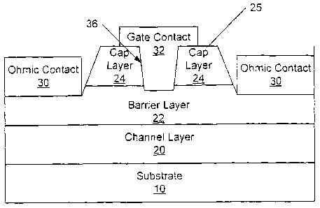
Figure 1A also illustrates a cap layer 24 on the barrier layer 22 with a gate
32
in a recess 36 through the cap layer 24. Figure 1B also illustrates a cap
layer 24' on
the barrier layer 22 with a gate 32 on the cap layer 24'. In some embodiments
of the
present invention, the cap layer 24, 24' is a non-uniform composition AlGaN
layer.
The cap layer 24, 24' moves the top (outer) surface of the device physically
away
from the channel, which may reduce the effect of the surface. The cap layer
24, 24'
may be blanket formed on the barrier layer 22 and may be epitaxially grown
and/or
formed by deposition. Typically, the cap layer 24, 24' may have a thickness of
from
about 2 nm to about 500 nm.
In some embodiments of the present invention, the cap layer 24, 24' may be a
graded AlGaN layer. The cap layer 24, 24' has an outer surface 25 that is
remote
from the barrier layer 22 where the amount of Al in the cap layer 24, 24'
adjacent the
surface is greater than an amount of Al in the cap layer 24, 24' in an
internal region of
the cap layer 24, 24'. For example, the cap layer 24, 24' may have a first
amount of
Al at the surface 25 and a second amount of aluminum in an internal region of
the cap
layer 24, 24' where the first amount is greater than the second amount. The
cap layer
24, 24' may also have a third amount of Al at the interface between the cap
layer 24,
24' and the barrier layer 22. The third amount may be greater than, less than
or equal
to the first amount. In particular embodiments of the present invention, the
AlGaN
cap layer 24, 24' includes a first region of Al,,Gai_XN at the surface 25,
where x<1 and
CA 02588114 2007-05-11
WO 2006/057686 PCT/US2005/031272
a second region of AlyGal_yN in an internal region of the cap layer 24, 24',
where y<x.
In some embodiments, x is from about 0.3 to about 1. In further embodiments, y
is
from about 0 to about 0.9. In particular embodiments, the AlGaN cap layer
includes a
third region of A1ZGa1_ZN at the interface between the barrier layer 22 and
the cap
layer 24, 24', where z<1 and z~y. Furthermore, z may be greater than y. For
example, in some embodiments of the present invention an A1N layer may be
provided as the barrier layer or a part of the cap layer adjacent the barrier
layer. In
such a case, the cap layer 24, 24' may include a graded Al concentration from
z to y
and from y to x. In particular embodiments of the present invention having a
gate
recessed through the cap layer 24, the higher concentration of Al extends into
the cap
layer from about 30 A to about 1000 A. In particular embodiments of the
present
invention having a gate on the cap layer 24', the higher concentration of Al
extends
into the cap layer from about 2.5 A to about 100 A.
The cap layer 24, 24' may be provided by conventional epitaxial growth
techniques where a higher Al concentration is provided during termination of
growth
of the cap layer 24, 24'. Thus, for example, the cap layer 24, 24' may be
provided by
MOCVD growth with an increase in the Al source just prior to and during
termination
of growth.
As is further illustrated in Figures 1A and 1B, ohmic contacts 30 are provided
on the barrier layer 22. A patterned mask and etch process may be used to
expose the
underlying barrier layer 22. In some embodiments of the present invention, the
etch
may be a low damage etch. In some embodiments of the present invention the
etch is
a wet etch with a strong base, such as KOH with UV illumination. In other
embodiments, the etch is a dry etch. Examples of low damage etch techniques
for
Group III-nitrides include etching techniques other than reactive ion etching,
such as
inductively coupled plasma using C12, BC13, CC12F2 and/or other chlorinated
species
or electron cyclotron resonance (ECR) and/or downstream plasma etching with no
DC
component to the plasma. As is further illustrated in Figures 1A and 1B, ohmic
metal
is patterned to provide ohmic contact material patterns that when annealed
provide the
ohmic contacts 30. While illustrated as recessed in Figures 1A and 1B, in some
embodiments of the present invention, the ohmic contacts 30 need not be
recessed.
As illustrated in Figure 1A, a gate recess may also be provided through the
cap layer 24 to expose a portion of the barrier layer 22. In some embodiments
of the
present invention, the recess 36 is formed to extend into the barrier layer
22. The
16
CA 02588114 2007-05-11
WO 2006/057686 PCT/US2005/031272
recess 36 may extend into the barrier layer 22 to, for example, adjust
performance
characteristics of the device such as threshold voltage, frequency
performance, etc.
The recess may be formed using a mask and an etch process as described above.
In
particular embodiments where the ohmic contacts 30 provide source and drain
contacts, the recess may be offset between the source and drain contacts such
that the
recess, and subsequently the gate contact 32, is closer to the source contact
than the
drain contact.
A gate contact 32 is formed in the recess and contacts the exposed portion of
the barrier layer 22. The gate contact may be a "T" gate as illustrated in
Figure 1A
and may be fabricated using conventional fabrication techniques. The gate
contact 32
may also be formed on the cap layer 24' as illustrated in Figure 1B and may be
fabricated using conventional fabrication techniques. Suitable gate materials
may
depend on the composition of the barrier layer, however, in certain
embodiments,
conventional materials capable of making a Schottky contact to a nitride based
semiconductor material may be used, such as Ni, Pt, NiSi, Cu, Pd, Cr, W and/or
WSiN.
A conventional passivation layer or a BN passivation layer as described below
may also be provided on the structures of Figures 1A and 1B. For example, a
SiN
layer and, in some embodiments, an extremely thin SiN layer, may be formed in
situ.
A MgN passivation layer, such as that described in U.S. Patent No. 6,498,111
entitled
"FABRICATION OF SEMICONDUCTOR MATERIALS AND DEVICES WITH
CONTROLLED ELECTRICAL CONDUCTIVITY," the disclosure of which is
incorporated herein by reference as if set forth in its entirety, could also
be utilized.
Optionally, an anneal of the structure including the passivation layer may be
carried
out in an oxygen environment to remove hydrogen from the layer and alter
surface
states and/or add oxygen to.the surface. If an oxygen anneal is performed, the
anneal
may be performed in a manner to not significantly oxidize the layer between
the
passivation layer and the underlying Group III-nitride layer. For example, in
some
embodiments of the present invention, the annealing may be carried out at a
temperature of from about 100 C to about 1000 C and for a time of from about
10
seconds to about 1 hour. The oxygen containing environment may be only oxygen,
oxygen in N2, oxygen in another inert gas, such as argon, oxygen in dry air,
CO, CO2,
NO, NO2 and/or ozone. The gases used to provide the oxygen containing
environment may be free of hydrogen so as to not incorporate hydrogen into the
17
CA 02588114 2007-05-11
WO 2006/057686 PCT/US2005/031272
passivation layer. Alternatively or additionally, an anneal may be carried out
in D2 or
D20.
Transistors according to embodiments of the present invention may be
fabricated utilizing techniques such as those discussed in the patent
applications and
patents incorporated by reference herein, including, for example, as described
in U. S.
Patent Application Serial No. 10/849,617, filed May 20, 2004 and entitled
"METHODS OF FABRICATING NITRIDE-BASED TRANSISTORS HAVING
REGROWN OHMIC CONTACT REGIONS AND NITRIDE-BASED TRANSISTORS
HAVING REGROWN OHMIC CONTACT REGIONS" and U.S. Patent Application
Serial No. 10/897,726, filed July 23, 2004 and entitled "METHODS OF
FABRICATING NITRIDE-BASED TRANSISTORS WITH A CAP LAYER AND A
RECESSED GATE," the disclosures of which are incorporated herein as if
described
in their entirety.
Figures 2A and 2B illustrate high electron mobility transistors having a cap
layer 34, 34' according to further embodiments of the present invention. The
substrate 10, channel layer 20, barrier layer 22, ohmic contacts 30 and gate
contact 32
may be provided as discussed above with reference to Figures lA and 1B. As
seen in
Figures 2A and 2B, the cap layer 34, 34' includes a doped region 40 at or near
the
outer surface of the cap layer 34, 34'. The cap layer 34, 34' may be a GaN
based cap
layer, such as a GaN layer and/or an AIGaN layer as described, for example, in
the
patents and patent application incorporated by reference herein. In some
embodiments of the present invention, the doped region 40 is doped with p-type
dopant, such as Mg, Be, Zn, Ca and/or C. In other embodiments of the present
invention, the doped region 40 is doped with an n-type dopant, such as Si, Ge
and/or
O. In further embodiments of the present invention, the doped region 40 is
doped
with a deep level dopant, such as Fe, C, V, Cr, Mn, Ni and/or Co. The dopant
may be
incorporated into the cap layer 34 during deposition or growth of the cap
layer 34, 34'
or may be subsequently implanted, for example, using ion implantation. In some
embodiments of the present invention, the cap layer 34 has a dopant
incorporated
throughout the cap layer 34, 34'. In such a case, the doped region 40 may be
provided
by a region of increased dopant concentration over the concentration of dopant
in the
remainder of the cap layer 34, 34'. Techniques for co-doping Group III-nitride
materials are described, for example, in United States Patent Application
Serial No.
10/752,970, filed January 7, 2004 entitled "CO-DOPING FOR FERMI LEVEL
18
CA 02588114 2007-05-11
WO 2006/057686 PCT/US2005/031272
CONTROL IN SEMI-INSULATING GROUP III NITRIDES," the disclosure of
which is incorporated herein as if set forth in its entirety.
In embodiments of the present invention where the dopants are n-type dopants,
the n-type dopants may be Si, Ge or O. In particular embodiments of the
present
invention without a gate recess, the doped region 40 extends into the cap
layer 34
from about 2.5 A to about 50 A. In particular embodiments of the present
invention
with a gate recess, the doped region 40 extends into the cap layer 34' from
about 20 A
to about 5000 A. With n-type dopants, the doped region 40 in embodiments
without a
gate recess may provide a dopant concentration of from about 1018 to about
1021 cm 3
and may be more heavily doped than 1021 cm 3 if a gate recess is provided. In
particular embodiments of the present invention, the doped region 40 may be
one or
more delta-doped regions at or near the surface of the cap layer 34, 34' and
may, for
example, have a dopant concentration of from about 10 11 to about 1015 cm 2.
As used
herein, a delta-doped region is at the surface if it is within about 5 A of
the surface
and near the surface if it is within about 50 A of the surface. In particular
embodiments of the present invention, the dopant is 0 that extends into the
cap layer
34, 34' about 20 A. N-type dopants may be used to screen the channel region
from
surface states and pin the surface energy level at a predictable and desired
level to
reduce and/or minimize trapping effects. The level of doping should be
sufficiently
high so as to be the dominant "surface" state in embodiments without a
recessed gate
but not so high as to provide excessive current leakage paths.
In other embodiments, the doped region 40 is a region doped with p-type
dopants. In particular embodiments of the present invention without a gate
recess, the
doped region 40 extends into the cap layer 34 from about 2.5 A to about 100 A.
In
particular embodiments of the present invention with a gate recess, the doped
region
40 extends into the cap layer 34' from about 30 A to about 5000 A. With p-type
dopants, the doped region 40 may provide a dopant concentration of from about
1016
to about 1022 cm 3. The p-type dopants may be Mg, Be, Zn, Ca and/or C. In
particular embodiments of the present invention, the doped region may be one
or
more delta-doped regions at or near the surface of the cap layer and may, for
example,
have a dopant concentration of from about 10ll to about 1015 cm"Z. P-type
dopants
may be used to screen the channel region from surface states, pin the surface
energy
level at a predictable and desired level to reduce and/or minimize trapping
effects and
to reduce leakage currents. The level of doping should be sufficiently high so
as to
19
CA 02588114 2007-05-11
WO 2006/057686 PCT/US2005/031272
reduce leakage current in embodiments without a recessed gate and be the
dominant
"surface" state but not so high as to provide introduce traps or leakage paths
by
becoming a conductive layer. However, in particular embodiments of the present
invention have a recessed gate as illustrated, for example, in Figure 2B, if
an
insulating region, such as a SiN layer or gap, is provided between the cap
layer 34'
and the gate contact 32, a high level of p-type dopants may be provided such
that the
cap layer 34' may be provided as a conductive layer.
Furthermore, in certain embodiments of the present invention, the doped
region 40 may be doped with p-type dopants so as to provide a p-n junction
between
the doped region and the cap layer 34 and the gate contact 32 is provided
directly on
the doped region 40 so as to provide a Junction HEMT (JHEMT). In such a case,
the
dope region 40 would not extend to the ohmic contacts 30, which may be
isolated
from the doped region by an insulating region, such as a SiN layer or gap.
In still further embodiments, the doped region 40 is a region doped with deep
level dopants. In particular embodiments of the present invention without a
gate
recess, the doped region 40 extends into the cap layer 34 from about 2.5 A to
about
100 A. In particular embodiments of the present invention with a gate recess,
the
doped region 40 extends into the cap layer 34' from about 30 A to about 5000
A.
With deep level dopants, the doped region 40 may provide a dopant
concentration of
from about 1016 to about 1022 cm-3. The deep level dopants may be Fe, C, V,
Cr, Mn,
Ni, Co or other rare earth elements. Deep level dopants may be used to screen
the
channel region from surface states, pin the surface energy level at a
predictable and
desired level to reduce and/or minimize trapping effects and to reduce leakage
currents. The level of doping should be sufficiently high so as to reduce
leakage
current in embodiments without a recessed gate and be the dominant "surface"
state
but not so high as to cause significant trapping.
Figures 3A and 3B illustrate electronic devices incorporating a graphitic
and/or amorphous BN passivation layer according to some embodiments of the
present invention. The substrate 10, channel layer 20, barrier layer 22, cap
layer 24,
ohmic contacts 30 and gate contact 32 may be provided as discussed above with
reference to Figures 1A, 1B and/or Figures 2A, 2B. As is further illustrated
in
Figures 3A and 3B, a graphitic and/or amorphous BN passivation layer 100, 100'
is
provided on exposed surfaces of the device. In particular embodiments of the
present
invention, the graphitic BN passivation layer 100, 100' is a non-single
crystal layer.
CA 02588114 2007-05-11
WO 2006/057686 PCT/US2005/031272
The graphitic and/or amorphous BN passivation layer 100, 100' may be provided
as a
single layer or may be multiple layers and may be incorporated with layers of
other
materials, such as SiN or SiOX. In particular embodiments of the present
invention the
graphitic or amorphous BN passivation layer 100 where the gate is recessed
through
the BN passivation layer 100, the BN passivation layer 100 may have a
thickness of
from about 3 A to about 1 m. In particular embodiments of the present
invention the
graphitic or amorphous BN passivation layer 100' where the gate is not
recessed
through the BN passivation layer 100', the BN passivation layer 100' may have
a
thickness of from about 2 A to about 100 A. Thus, in the embodiments
illustrated in
Figure 3B, a MISHEMT may be provided. Furthermore, as discussed above, the
gate
may be recessed into or through the cap layer 24 as illustrated, for example,
in
Figures 1A and 2B, and the BN passivation layer 100, 100' may extend into the
recess in the cap layer 24, into the recess and onto the barrier layer 22 or
may
terminate at the gate contact 32. Thus, in some embodiments of the present
invention
a MISHEMT may be provided with a recessed gate.
Techniques for forming graphitic and/or amorphous BN, such as by MOCVD,
are lcnown to those of skill in the art and, therefore, need not be described
further
herein. For example, a BN layer may be formed by flowing TEB and NH3 in a
carrier
gas. However, the formation of the graphitic and/or amorphous BN passivation
layer
100 should be carried out at temperatures below the decomposition temperature
of the
underlying structure on which the passivation layer 100 is formed. Thus, for
example,
for a GaN based structure, the graphitic and/or amorphous BN passivation layer
100
should be formed at temperatures of less than about 1100 C and in some
embodiments less than about 950 C. In some embodiments, the passivation layer
100 may be subsequently annealed as described above.
Figures 4A and 4B illustrate electronic devices incorporating a SiC
passivation layer according to some embodiments of the present invention. The
substrate 10, channel layer 20, barrier layer 22, cap layer 24, ohmic contacts
30 and
gate contact 32 may be provided as discussed above with reference to Figures
1A, 1B
and/or Figures 2A, 2B. As is further illustrated in Figures 4A and 4B, a SiC
passivation layer 110, 110' is provided on exposed surfaces of the device. In
particular embodiments of the present invention, the SiC passivation layer
110, 110' is
a non-single crystal layer. In some embodiments of the present invention, the
SiC
passivation layer 110, 110' is insulating or p-type SiC. If the SiC
passivation layer,
21
CA 02588114 2007-05-11
WO 2006/057686 PCT/US2005/031272
110' is p-type SiC, an insulating region, such as a SiN layer or a gap, may be
provided
between the SiC passivation layer 110, 110' and the ohmic contacts 32. In some
embodiments of the present invention, the SiC passivation layer 110, 110' is
3C SiC
as 3C SiC may be formed on on-axis (0001) hexagonal materials in a low
temperature
process. The SiC passivation layer 110, 110' may be provided as a single layer
or
may be multiple layers and may be incorporated with layers of other materials,
such
as SiN or Si02. In particular embodiments of the present invention the SiC
passivation layer 110 where the gate is recessed through the SiC passivation
layer
110, the SiC passivation layer 110 may have a thickness of from about 3 A to
about 1
m. In particular embodiments of the present invention the SiC passivation
layer 110'
where the gate is not recessed through the SiC passivation layer 110', the SiC
passivation layer 110' may have a thickness of from about 2 A to about 100 A.
Thus,
in the embodiments illustrated in Figure 4B, a MISHEMT may be provided.
Furthermore, as discussed above, the gate may be recessed into or through the
cap
layer 24 as illustrated, for example, in Figures 1A and 2B, and the SiC
passivation
layer 110, 110' may extend into the recess in the cap layer 24, into the
recess and onto
the barrier layer 22 or may terminate at the gate contact 32. Thus, in some
embodiments of the present invention a MISHEMT may be provided with a recessed
gate.
Techniques for forming SiC layers are known to those of skill in the art and,
therefore, need not be described further herein. However, the formation of the
SiC
passivation layer 110 should be carried out at temperatures below the
decomposition
temperature of the underlying structure on which the passivation layer 110 is
formed.
Thus, for example, for a GaN based structure, the SiC passivation layer 110
should be
formed at temperatures of less than about 1100 C and in some embodiments less
than
about 950 C. Techniques for forming SiC at such low temperatures may include
CVD or PECVD using, for example, SiH4 and C3H8 as Si and C sources, or very
low
temperature sputtering. Furthermore, the SiC layer may be doped with
impurities to
control the properties of the SiC passivation layer 110. For example, n-type
SiC may
be doped with N, p-type SiC may be doped with Al and/or B and insulating SiC
may
be doped with V or Fe. In some embodiments, the passivation layer 100 may be
subsequently annealed as described above.
While Figures 3A, 3B and 4A, 4B illustrate passivation layers 100,100' and
110, 110' on a cap layer 24, other cap layers, such as the cap layer 34,
conventional
22
CA 02588114 2007-05-11
WO 2006/057686 PCT/US2005/031272
single or multiple cap layers or no cap layer may be provided. For example,
the
passivation layers 100, 100' and 110, 110' could be used with a cap layer that
included an A1N layer at its outer surface such that the passivation layers
were
provided on the A1N layer. Thus, the use of a graphitic or amorphous BN
passivation
layer 100, 100' or a SiC passivation layer 110, 110' should not be construed
as limited
to the particular structure illustrated in Figures 3A, 3B and 4A, 4B but may
be used
on any Group III-nitride semiconductor device or other wide bandgap
semiconductor
device.
While embodiments of the present have been described with reference to
HEMT structures where the gate is directly on the barrier or cap layers, in
some
embodiments of the present invention an insulating layer may be provided
between
the gate and the barrier or cap layer. Thus, in some embodiments of the
present
invention, an insulating gate HEMT may be provided, for example, as described
in
U.S. Patent Publication No. 2003/0020092 entitled "INSULATING GATE
ALGAN/GAN HEMT", to Parikh et al., the disclosure of which is incorporated
herein
by reference as if set forth fully herein. In some embodiments, the insulating
layer
may be of graphitic and/or amorphous BN.
Figures 5A and 5B illustrate further embodiments of the present invention
incorporating an A1N cap layer 54, 54'. Figure 5A also illustrates an AIN cap
layer
54 on the barrier layer 22 with a recessed gate 32 through the A1N cap layer
54.
Figure 5B also illustrates an AIN cap layer 54' on the barrier layer 22 with a
gate 32
on the A1N cap layer 54'. The cap layer 54, 54' moves the top (outer) surface
of the
device physically away from the channel, which may reduce the effect of the
surface.
Furthermore, the A1N cap layer 54, 54' may provide increased chemical
stability and
protect the underlying layers in that the AIN cap layer 54, 54' may not be
susceptible
to etching or other chemical reactions at high temperatures due to the
stronger Al-N
bonds compared to Ga-N bonds.
The A1N cap layer 54, 54' may be blanket formed on the barrier layer 22 and
may be epitaxially grown and/or formed by deposition. Typically, the cap layer
54,
54' may have a thickness of from about 0.2 nm to about 500 nm. In particular
embodiments of the present invention having a gate recessed through the A1N
cap
layer 54, the A1N cap layer 54 has a thickness of from about 10 A to about
5000 A. In
particular embodiments of the present invention having a gate on the AIN cap
layer
54', the A1N cap layer 54' has a thickness of from about 2 A to about 50 A.
23
CA 02588114 2007-05-11
WO 2006/057686 PCT/US2005/031272
The AIN cap layer 54, 54' may be provided by conventional epitaxial growth
techniques by termination of the Ga source during termination of growth of the
barrier
layer 22. Thus, for example, the AIN cap layer 54, 54' may be provided by
MOCVD
growth by termination of the Ga source just prior to and during termination of
growth.
Figure 6 illustrates further embodiments of the present invention where a
protective layer 64 is provided on the barrier layer 22. As is illustrated in
Figure 6,
the ohmic contacts are provided on the protective layer 64. The gate contact
32 may
also be provided on the protective layer 64. In certain embodiments of the
present
invention, the ohmic contacts 30 are provided directly on the protective layer
64 and
the gate contact 32 may also be provided directly on the protective layer 64.
The protective layer 64 may be a SiN layer deposited prior to formation of the
ohmic contacts 30 and the gate contact 32. Alternatively, the protective layer
64 may
be a BN or MgN layer. MgN may be especially suitable for use with p-type
devices
as additional doping may be provided upon anneal of the ohmic contact
material. The
protective layer 64 may be a single layer, such as a single SiN, MgN or BN
layer, or,
in some embodiments, protective layer 64 may be provided as multiple layers,
such as
a layer of SiN and a layer of A1N.
The protective layer 64 may have a thickness of from about I A to about 10
A and, in some embodiments, may have a thickness of about one monolayer.
Because the protective layer 64 is thin, there may be no need to recess the
ohmic
contacts through the protective layer 64. Reliability may be improved through
better
surface state control and lower gate leakage current in comparison to devices
without
such a protective layer.
The protective layer 64 may be formed in-situ with the formation of the
barrier
layer. Because the protective layer 64 is very thin, there may be very little
additional
fabrication cost other than providing a Si source, B source or Mg source and
only a
small additional growth time to deposit the thin protective layer 64.
Furthermore,
because the protective layer 64 is thin, no additional steps may be needed to
form
recesses for the gate and/or ohmic contacts.
While embodiments of the present invention have been described herein with
reference to particular HEMT structures, the present invention should not be
construed as limited to such structures. For example, additional layers may be
included in the HEMT device while still benefiting from the teachings of the
present
invention. Such additional layers may include GaN cap layers, as for example,
1 24
CA 02588114 2007-05-11
WO 2006/057686 PCT/US2005/031272
described in Yu et al., "Schottky barrier engineering in III-V nitrides via
the
piezoelectric effect," Applied Physics Letters, Vol. 73, No. 13, 1998, or in
U.S. Patent
Publication No. 2002/0066908A1 filed July 12, 2001 and published June 6, 2002,
for
"ALUMINUM GALLIUM NITRIDE/GALLIUM NITRIDE HIGH ELECTRON
MOBILITY TRANSISTORS HAVING A GATE CONTACT ON A GALLIUM
NITRIDE BASED CAP SEGMENT AND METHODS OF FABRICATING SAME,"
the disclosures of which are incorporated herein by reference as if set forth
fully
herein. In some embodiments, insulating layers such as SiN, an ONO structure
or
relatively high quality A1N may be deposited for making a MISHEMT and/or
passivating the surface. The additional layers may also include a
compositionally
graded transition layer or layers.
Furthermore, the barrier layer 22 may also be provided with multiple layers as
described in U.S. Patent Publication No. 2002/0167023A1 cited above. Thus,
embodiments of the present invention should not be construed as limiting the
barrier
layer to a single layer but may include, for exainple, barrier layers having
combinations of GaN, AlGaN and/or A1N layers. For example, a GaN, A1N
structure
may be utilized to reduce or prevent alloy scattering. Thus, embodiments of
the
present invention may include nitride based barrier layers, such nitride based
barrier
layers may include AlGaN based barriei layers, AIN based barrier layers and
combinations thereof.
While embodiments of the present invention have been described with
reference to the ohmic contacts 30 being recessed through the various cap
layers, in
certain embodiments of the present invention, the ohmic contacts 30 are
provided on
the cap layer or only partially recessed into the cap layer. Thus, embodiments
of the
present invention should not be construed as limited to structures having
ohmic
contacts recessed through the cap layer.
In the drawings and specification, there have been disclosed typical
embodiments of the invention, and, although specific terms have been employed,
they
have been used in a generic and descriptive sense only and not for purposes of
limitation.