Note : Les descriptions sont présentées dans la langue officielle dans laquelle elles ont été soumises.
CA 02588313 2015-01-13
CONTACT FOR USE IN TESTING INTEGRATED CIRCUITS
Technical Field
The present invention deals broadly with testers for
evaluating integrated circuit devices and structure for mating
leads of the integrated circuit device to corresponding pads
of a load board that interfaces with the tester. More
narrowly, however, it deals with contacts positioned in an
array for electrically connecting the integrated circuit leads
with their corresponding load board pads and providing
structure for efficiently transmitting test signals. A
specific focus of the invention is a particular contact to be
used in such an array in order to maintain impedance at a
desired level.
Background of the Invention
Integrated circuit tester devices have long been used in
industry to test and evaluate the quality of the device being
tested. Signal integrity is, of course, an important
1
CA 02588313 2007-05-11
consideration in conducting testing. It is also desirable to
maintain impedance through a conducting portion of a contact
interconnecting the integrated circuit lead to its
corresponding load board pad at a particular desired level.
For example, in the case of testing of many types of devices,
50 ohms is a desired level.
The impedance that is achieved is a function of a number
of factors. These include length of conduction path, material
of which the conductive structure is made, etc.
The present invention is a contact which improves the
testing function beyond what is achieved with other contacts.
It takes into consideration the dictates of the prior art and
overcomes problems extant therein.
Summary of the Invention
The invention is a contact which spans a space which
separates a lead of an integrated circuit to be tested by a
tester apparatus and a pad of a load board interfacing with
the tester. The contact thereby provides electrical
communication between the integrated circuit lead and the load
board pad. The contact includes an insulating lamina which has
oppositely facing sides and a profile which includes a first
end engageable by the lead of the integrated circuit. The
profile also has a second end which is in engagement with a
pad of the load board. A conductive lamina overlies at least a
2
CA 02588313 2007-05-11
portion of the insulating lamina. The conductive lamina also
extends from the first end of the insulating lamina to the
second end thereof. The thickness of the conductive lamina is
expanded at the first and second ends of the insulating
lamina. Consequently, a first end of the conductive lamina is
more effectively engaged by the lead of the integrated
circuit, and a second end of the conductive lamina, proximate
the load board, more effectively engages the pad of the load
board.
In one embodiment of the invention, the conductive lamina
comprises a first trace which is applied to one side of the
insulating lamina. This first conductive trace extends from
the first end of the insulating lamina to its second end. This
embodiment also includes a second conductive trace which
overlies at least a part of the other side of the insulating
lamina and also extends from the first end to the second end
of that lamina. In a preferred embodiment, the first and
second conductive traces extend beyond the first end of the
insulating lamina and include means, extending from the
conductive traces, for cutting through oxide build-up on the
lead of the integrated circuit which engages the contact.
Typically, tin oxide will build up on the surface of the
integrated circuit device lead.
The means for cutting through an oxide build-up, it is
intended, would include an elongated blade edge. Such a blade
3
CA 02588313 2007-05-11
edge would extend from each conductive trace at its first or
upper end. In one envisioned construction, these blade edges
would extend generally parallel to one another. Similarly,
they would, in turn, be generally parallel to a plane defined
by a surface of the contact. Because of intended elastomeric
mounting of the contact, the blade edges, when engaged by a
lead of an integrated circuit, would move linearly in a
direction of the lay of the blade edges when they are not
engaged by an integrated circuit.
It will be understood that the conductive laminae or
traces can be either sandwiched between lateral insulating
layers or together, sandwich an insulating layer between two
conductive laminae. The specific construction would, of
course, depend upon the application of the tester, whether the
housing in which the elastomeric mounting of the contact was
accomplished were metallic, etc.
Certain embodiments of the invention can provide for
redundant contacting. Such a concept could enable reduction in
size of components to support pitch lower than 0.5 mm. With
use of a ceramic insulating material, the effects E-field
radiating could be greatly reduced or eliminated.
It is envisioned that the insulating lamina would be made
of a ceramic material. It has been found that such a material
tends to be the best of a number of choices to serve such a
purpose.
4
CA 02588313 2007-05-11
The present invention is thus an improved contact for use
in integrated circuit testing. More specific features and
advantages obtained in view of those features will become
apparent with reference to the DETAILED DESCRIPTION OF THE
INVENTION, appended claims and accompanying drawing figures.
Brief Description of the Drawings
FIG. 1 is a side elevational view of a portion of a set
of contacts in accordance with the present invention spanning
a space between, and interconnecting, corresponding leads of
an integrated circuit device and corresponding pads of a load
board which interfaces with a tester;
FIG. 2 is a perspective view of the portion illustrated
in FIG. 1;
FIG. 3 is a side elevational view of a ceramic lamina
contact having conductive trace material plated on a side of
the contact;
FIG. 4 is a perspective view of a further embodiment of
the invention illustrating a ceramic contact array wherein a
controlled impedance trace is sandwiched between two
nonconductive layers;
FIG. 5 is a view similar to FIG. 4 but illustrating full
pad interface;
FIG. 6 is a view similar to FIG. 1 illustrating the
second embodiment of the invention;
5
CA 02588313 2007-05-11
FIG. 7 is an elevational view illustrating a third
contact embodiment interconnecting the integrated circuit lead
and the load board pad;
FIG. 8 is a view similar to FIG. 2 illustrating a contact
including an attached decoupling component; and
FIG. 9 is a side elevational view of the contact of FIG.
8.
Detailed Description of the Invention
Referring now to the drawing figures wherein like
reference numerals denote like elements throughout the several
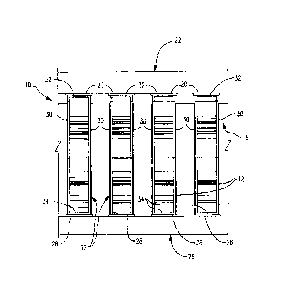
views, FIG. 2 illustrates a contact array 10 for use in a test
socket. Such an array 10 employing contacts 12 in accordance
with the present invention uses substantially cylindrical
elastomers 14, 16 to mount the contacts 12 to a housing 18.
The housing 18, in turn, enables contacts to span the distance
between leads 20 of an integrated circuit device 22 to be
tested, when the device is in an appropriate location, and
pads 24 on a load board 26 which interfaces with the tester
apparatus (not shown). FIG. 2 illustrates a segment of a test
socket mounting four contact elements. It will be understood,
of course, that this number is not exclusive. In fact, the
typical integrated circuit will dictate the employment of
considerably more contacts so that at least one contact will
be present to provide electrical signal transmission between
6
CA 02588313 2007-05-11
each lead 20 of the integrated circuit device 22 and its
corresponding load board pad 24.
The contact set illustrated in FIG. 2 is shown in more
detail in FIG. 1. Each contact 12 is provided with an
insulating lamina 28. The lamina 28, in turn, has a conductive
trace 30 applied to each of opposite sides thereof. A trace 30
is applied in an overlying relationship to at least a portion
of the insulating lamina 28 and extends from a first end 32 of
the insulating lamina 28 to a second end 34 thereof. FIG. 3
illustrates a trace 30 which generally takes the form of a
band 36 applied to a ceramic insulating lamina so that, when
an integrated circuit 22 is engaged with upper ends of the
contacts 12 comprising the array 10, an electrical path will
be provided between each integrated circuit lead 20 and the
corresponding load board pad 24. Such a band 36 can be of any
width or length to match impedance of the device I/O. Its
width can also vary to generate stubs (not shown) that could
optimally match device I/O to a certain impedance or represent
an inductive or capacitive element.
It will be understood that a symmetrical trace 30 would
be applied to the other side of the contact insulating lamina
28 also. Symmetry of the traces 30 will afford a substantially
identical redundancy.
As seen in FIG. 1, the point of engagement of the contact
with the lead 20 of the integrated circuit 22 is conductive.
7
CA 02588313 2007-05-11
Similarly, FIG. 1 illustrates contact 12 with the load board
pad 24 as having a width substantially as great as the ceramic
insulating lamina 28. As a result, signals will be transmitted
through the contact 12 in an efficient manner. Again, the
symmetry of the traces 30 on opposite sides of the same
contact insulating lamina 28 will provide substantially the
same response irrespective of signal transmission path.
The type of ceramic material selected and the material
and geometry of the traces 30 are chosen in order to achieve a
desired impedance. In a particular application, an impedance
of 50 ohms is desirable. The shape and route of the traces 30
can be varied, as necessary, to achieve the impedance desired.
Further, a decoupling component 38 could be mounted on the
contact trace 30 to create a smart contact which would allow
for production testing mimicking real-world applications.
Further, the relative location of the traces 30 on the
insulating lamina 28 would facilitate the accommodation of
smaller pitch devices. Thus, the particular shape, size and
orientation of traces 30 are factors to be considered in
creating the contacts 12.
FIGS. 4 and 5 illustrate, in different degrees of pad
interfacing, a second contact embodiment array. Mounting of
each contact 12 is similar to that employed in mounting the
embodiment previously discussed. FIG. 4 is a view illustrating
a recessed pad construction. FIG. 5 is a view illustrating
8
CA 02588313 2007-05-11
full pad interface. Components are, otherwise, substantially
the same as components illustrated in FIGS. 1 and 2.
FIG. 6 illustrates a series of contacts 12 wherein the
conductive trace 30 is interior to the contact 12. That is,
the trace is laterally central in the contact 12 with
nonconductive laminae 40, 40' sandwiching the conductive trace
30 therebetween. At ends of the traces 30, however, engagement
portions 42, 44, extending generally normal to a plane defined
by the internal trace 30, is provided. One transverse portion
42 is engaged by the lead 20 of the integrated circuit device
22, and another transverse portion 44 engages a corresponding
load board pad 24. Such a contact construction offers
variation in design in view of desired impedance, facilitation
of good inter-engagement and significant signal transmission.
The conductive portion of a contact so constructed is
physically separated farther from an adjacent contact's
conductive portion. This results in improved crosstalk
performance. The "I-beam" construction is structurally strong
and will result in enhanced mechanical performance. The top
and bottom portions 42, 44 can be recessed from edges to
accommodate recessed device I/O leads 20 and result in the
contact being able to be incorporated into a totally metal
housing for improved thermal and ground inductance.
9
CA 02588313 2007-05-11
Again, FIGS. 8 and 9 illustrate the application of a
decoupling component 38. The construction and advantages of
such an embodiment are discussed hereinbefore.
FIG. 7 illustrates a further embodiment of a contact in
accordance with the present invention. In some degree, the
contact of FIG. 7 is similar to the contacts shown in FIG. 6.
That is, nonconductive laminae 40, 40' sandwich a conductive
trace element 30 therebetween. In fact, however, the contact
of FIG. 7 is a hybrid of the contacts of FIG. 1 and FIG. 6.
That is so because a central core 46 is provided from a
nonconductive ceramic material. Dual traces 30, 30' are
applied to oppositely-facing sides of the central core 46, and
the nonconductive side components 40, 40' are overlain to
complete the contact. In this embodiment, however, means for
cutting through oxide build-up on the integrated circuit
device lead are provided. Such means can take the form of an
elongated blade edge 48, 48' extending from one or both of the
conductive traces 30, 30'. As seen best in FIG. 7, the blade-
like elements 48, 48' extend distally with respect to the
traces 30, 30' and are engaged by a lead 20 of the integrated
circuit device 22. Typically the device leads 20 are made of
matte tin. When this material is used for the leads, tin oxide
can build up and diminish the integrity of operation of the
contact transmission element. Because of the blade edges 48,
48' of the traces 30, 30', a very fine etch through the tin
CA 02588313 2007-05-11
,
,
oxide will occur and the integrity of signal transmission will
not be diminished. The blade edge size can be increased or the
radius changed to adjust and control the forces applied to the
device I/O to minimally break through tin oxides without
creating damage to the device I/O leads 20.
It will be understood that the degree of pressure with
which the blade edges 48, 48' are applied to the tin oxide is
a function of the elastomers 14, 16 by which the contacts 12
are mounted. Appropriate elastomers will be selected depending
upon the degree of oxidation of the integrated circuit leads
and other factors.
As will be seen, the present inventive concept includes
use of a ceramic material to form one or more laminae of a
transmission contact 12 with one or more conductive traces 30,
30' applied to nonconductive ceramic portions. By varying the
laminar structure, the size, shape and other features of the
traces and other factors, a desired impedance level can be
achieved. Conductive traces and the particular construction
involved enables a contact 12 to be used with recessed pad
devices or, when the ceramic laminae are manipulated, with
metal housings. In consequence, the electrical match,
inductance and crosstalk are improved. The principles involved
can be applied when using a greater than air dielectric
material to plate surfaces of a contact. Again, matching
characteristics and greatly reduced signal propagation to
11
CA 02588313 2015-01-13
other contacts in the housing structure will be improved. That
is, crosstalk will be reduced.
12