Note : Les descriptions sont présentées dans la langue officielle dans laquelle elles ont été soumises.
CA 02592899 2007-07-03
WO 2006/058196 PCT/US2005/042709
METHOD AND APPARATUS FOR LED BASED MODULAR DISPLAY
RELATED APPLICATION
[0001] This patent application claims priority of U.S. Provisional Application
Serial No.
60/631236 filed November 26, 2004 titled "Method and Apparatus for LED Based
Modular Display ",
which is hereby incorporated herein by reference. This patent application
claims priority of U.S.
Application Serial No. [not yet assigned] filed November 23, 2005 titled
"Method and Apparatus for
LED Based Modular Display ", which is hereby incorporated herein by reference.
This patent
application is related to U.S. Application Serial No. 10/810300 filed March
26, 2004 titled "Method
and Apparatus for Light Emitting Devices Based Display", U.S. Provisional
Application Serial No.
60/584920, and U.S. Provisional Application Serial No. 60/591110.
FIELD OF THE INVENTION
[0002] The present invention pertains to a method and apparatus for a light
emitting device (LED)
based modular display. More particularly, the present invention relates to a
method and apparatus for a
large area LED based electronic display composed of a plurality of smaller LED
based display modules
(tiles) that are mounted to create a large display.
BACKGROUND OF THE INVENTION
[0003] Large tiled displays have been built using CRTs, backlit LCD displays
and projection
displays. Projection displays are the most popular form of tiled displays in
use today. However, there
are significant problems to building large tiled displays using projection
technologies. For example,
each projector has a slightly different color gamut caused by variations in
the light bulb, the color
filters, and the digital processing (contrast, brightness and gamma) for each
projector.
[0004] On the other hand, LED arrays can be made very precisely with respect
to specifications of
the color wavelength required. It is now possible to match the wavelengths of
the output light to within
+/-3nm. The liglit output from the LEDs is "purer" than the red, green, or
blue light output of a lamp
and color filters, and has a half power bandwidth of less than 30nm.
[0005] LED based displays are increasingly taking over the markets for large
displays used
outdoors and 'ui public areas, such as, airports and shopping malls. LEDs have
long life times
compared with projection bulbs and have excellent color performance. LEDs can
be manufactured to
provide deeper reds, 635 nm, for example, than is possible with the standard
red phosphors (615 nm)
used in the NTSC standards based CRT displays. In addition, LEDs have a very
high dynamic range
leading to excellent color performance.
[0006] The displays that are presently being constructed and used employ
individually mounted
red, green and blue LEDs or modules having a small array of red, green, and
blue LEDs. Figure 3
CA 02592899 2007-07-03
WO 2006/058196 PCT/US2005/042709
(Prior Art) shows an M x N display built using M x N RGB LED pixel units. Each
RGB pixel unit
needs a minimum of one red, one green, and one blue LED. Sometimes a single
pixel unit is built with
2 red LEDs, 2 green LEDs and 1 blue LED. This is done, for example, in the
LEDTRONICS RGB-
1006-001 2 x 2 pixel module that contains 8 red, 8 green and 4 blue LEDs. Some
manufacturers use a
single red, green, and blue for an RGB pixel. To display a white color for a
particular pixel the
luminance value of the red, green, and blue LEDs are driven in the ratio of
0.3, 0.59, and 0.11
respectively. For ease in building large displays, smaller standard modules
varying widely in size are
used. A few representative samples are, for example, an 8 x 8 pixel unit from
LEDTRONICS model
RGB-1004-002 where the pixel pitch is 6mm and the module size is 47.8 mm x
47.8 mm. BARCO,
INC. has a unit, the MiPix-20 a 2 x 2 pixel module that has a pixel pitch of
20 mm and the module is
40.3 mm x 40.3 mm. An example of a larger module is one from Daktronics, Inc.,
the AF 5010.series
16 x 16 pixel modules with a pixel pitch of 23 mm and a size of 365 mm x 365
mm.
[0007] To reduce the wiring and complexity in driving individual LEDs, the
LEDs in a module
are pre-wired to be configured in the common anode or common cathode
configuration. The finished
display consisting of hundreds of thousands of modules is then energized by
scanning the rows or
colunms or a combination of rows and columns. A representative example of the
complexity of such
large LED displays is shown by the Coca-Cola display in Times Square in New
York City which was
built by Daktronics, Inc. The display consists of 882,112 LED pixels, using
2,646,336 LED diodes, and
over 80,000 feet of wiring. This may present a problem.
[0008] One can see that the present approaches for creating LED displays is
very costly and
overly complicated. Another disadvantage of the present approaches is that the
viewer can often see
the individual red, green, and blue subpixels. This may present a problem.
2
CA 02592899 2007-07-03
WO 2006/058196 PCT/US2005/042709
BRIEF DESCRIPTION OF THE DRAWINGS
[0009] The invention is illustrated by way of example and not limitation in
the figures of the
accompanying drawings in which:
[0010] Figure 1 illustrates a network environment in which the present
invention may be
implemented;
[0011] Figure 2 is a block diagram of a computer system which may be used for
implementing
some embodiments of the invention;
[0012] Figure 3 shows a prior approach;
[0013] Figure 4 shows one embodiment of the present invention showing an LED
display engine
using colunms of Red, Green and Blue LEDs;
[0014] Figure 5A shows one embodiment of the present invention illustrating a
block diagram of a
modular LED display;
[0015] Figure 5B shows one embodiment of the present invention illustrating a
cross-section of a
modular LED display;
[0016] Figure 6 shows one embodiment of the present invention in block diagram
illustrating a
large LED display built from smaller LED display modules;
[0017] Figure 7 shows one embodiment of the present invention showing more
details in block
diagram form;
[0018] Figure 8 shows one embodiment of the present invention illustrating an
LED display
engine using a substrate with multiple columns of RGB LEDs and a rotating
mirror;
[0019] Figure 9 shows in flowchart form, for one embodiment of the invention,
the procedure for
alignment of top and bottom pixels to the screen edge;
[0020] Figure 10 shows one embodiment of the invention illustrating the fmal
assembly of LED
display modules and adjustment procedures;
[0021] Figure 11 shows one embodiment of the invention illustrating a large
LED display built
with smaller LED modules; and
[0022] Figure 12 shows one embodiment of the invention illustrating a
configuration where
adjacent modules have motion in opposite directions.
3
CA 02592899 2007-07-03
WO 2006/058196 PCT/US2005/042709
DETAILED DESCRIPTION
[0023] As used in this description, "LED" or similar terms refers to light
emitting devices. There
are a variety of light emitting devices, for example, light emitting diodes
(commonly referred to as
LEDs), visible light emitting lasers, vertical cavity surface emitting lasers
(VCSELs), quantum dots,
resonant cavity light emitting diodes (RCLEDs), organic light emitting diodes
(OLEDs),
electroluminescent diodes (ELDs), photon recycling semiconductor light
emitting diode, etc. For
convenience in illustrating various embodiments of the invention, LED and
similar terins will refer to
all such Light Emitting Devices, not to just light emitting diodes. That is,
our use of LED here
includes, light emitting diodes, lasers, etc. Where a distinction is made the
text will explicitly use a
specific term intended.
[0024] In various embodiments of the present invention, the invention utilizes
techniques that
have been developed for constructing tiled LED based displays in which the
seams between the tiles
are virtually imperceptible to the human eye under normal viewing conditions.
[0025] In one embodiment of the present invention, a large LED display may be
built using
smaller modules. The modules are built using LEDs in much smaller numbers than
would be required
if individual LEDs were used for each pixel (for example, as described in U.S.
Patent Application
Serial No. 10/810300 filed March 26, 2004 titled "Method and Apparatus for
Light Emitting Devices
Based Display", U.S. Provisional Application Serial No. 60/584920, and U.S.
Provisional Application
Serial No. 60/591110). One representative example of this approach creates a
1.2 ft. x 1.2 ft. display
module providing a resolution of 256 x 256 pixels and uses in one embodiment
256 x 3 (768) LEDs
and in another embodiment uses 256 x 3 x 2 (1536) LEDs instead of the usua1256
x 256 x 3 (196,608)
LEDs that would be required for a dedicated LED array. Given the reduced
number of LEDs used, this
approach may reduce the cost and complexity of the display. Additionally,
since the pixel position is
related to when LEDs are energized in time, in one embodiment, the display
image created does not
have red, green and blue subpixels that are discernable by the human eye.
[0026] In one embodiment of the invention, a large display is built up using
the LED display
modules described above. The modules are carefully placed so that they are
close to (or possibly
touching) each other and are aligned top and bottom and on the sides. The
tiled display needs to have a
nearly invisible joint (seam) between the tiles to be widely acceptable to
users. There are 2 conditions
that need to be met in order to achieve this:
1. The interpixel gap should be visually identical within and between tiles;
and
2. The angular distribution of the intensity of liglit emitted from a tile
should be the same at the
left and right and at the top and bottom edges of a tile.
[0027] In one embodiment of the present invention, the 2 conditions mentioned
above are
achieved by adjusting the start and end times of the energization of the LEDs.
This adjustment is
checked when a module is constructed and is re-checked when the display is
assembled with the
individual modules. This takes care of the vertical seams or pixels at the
columns on the 2 vertical sides
4
CA 02592899 2007-07-03
WO 2006/058196 PCT/US2005/042709
of the modules. The horizontal seams are taken care of by construction. During
assembly of the
module, the distance to the screen from the optics is adjusted until the
pixels at the top edge are aligned
to the top edge, and the pixels at the bottom edge are aligned to the bottom
edge. The uniform
brightness requirement is met by lighting up adjacent tiles with a suitable
pattern and the intensity is
measured. An adjustment is made, if necessary, to reduce the brightness of the
brighter module by
turning down the brightness by a reduction factor. This reduction factor may
be stored in the non-
volatile memory of each of the relevant modules, or may be downloaded at
startup, or dynamically
adjusted periodically during operation.
[0028] Figure 1 illustrates a network environment 100 in which the techniques
described may be
applied. More details are described below.
[0029] Figure 2 illustrates a computer system 200 in block diagram form, which
may be
representative of any of the devices shown in Figure 1. More details are
described below.
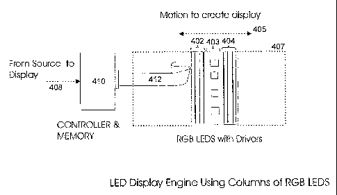
[0030] Figure 4 shows an embodiment of a LED display engine 400 using columns
of RGB LEDs
(402, and 404). The columns of LEDs (402, and 404) are driven by drivers 403.
The LEDs (402, 404)
and drivers 403 are moved 405 to cover an area 407. An input source 408
communicates with a
controller and memory 410 which communicates via 412 with the drivers 403.
This type of
embodiment is described in detail in U.S. Application Serial No. 10/810300
filed March 26, 2004 titled
"Method and Apparatus for Light Emitting Devices Based Display", U.S.
Provisional Application
Serial No. 60/584920, and U.S. Provisional Application Serial No. 60/591110.
[0031] Figure 5A is a block diagram 500 of one embodiment of a modular LED
display. RGB
digital video information 501 is sent from the Controller and Director to the
display module. The
relevant LED drive signals together with the timing information are fed to the
LED display engine 502.
This may be the engine in Figure 4, Figure 7, the alternate engine shown in
Figure 8, or another engine.
The LED display engine 502 creates an image of the display to be handled by
this module albeit in a
smaller size. This image is communicated 503 to a magnification means, such as
magnified by the
magnifying optics of one or more multi-element aspheric lens 504. These lenses
may be made of glass
or optical grade plastics. The lenses are designed to minimize distortions,
especially cliromatic
aberrations. These converging rays of the image are communicated 505 and
impinge on a screen, such
as a non-glare acrylic Fresnel lens screen 506. The Fresnel lens is designed
to converge the diverging
rays so that they come out substantially perpendicular to the screen.
[0032] Figure 5B shows one embodiment of the invention 550 showing how a
module is
assembled in a suitable frame to achieve a cross-section. The LED display
engine 552 produces a
display that is communicated to the magnifying optics 554 which communicates
the image from the
display engine 552 to the acrylic Fresnel lens screen 556. The lens
subassembly (including the
magnifying optics 554) is assembled in the mechanical package at the nominal
position to create the
required magnification on the screen 556. There are adjusting means (such as
screws) to change the
distance from the LED display engine 552 to the magnifying optics 554
subassembly ("a") and the
CA 02592899 2007-07-03
WO 2006/058196 PCT/US2005/042709
distance from the screen 556 to the lenses 554 ("b"). A later discussion will
detail the need for
adjusting distances "a" and "b".
[0033] In one embodiment of the invention, to minimize the thickness of the
modules, and in
addition, to get the maximum luminance at the screen, the magnifying lenses
are designed to have a
low f number. The total thickness of the module is constrained by the fact
that the wider the angle of
the lens the lower the illumination at the edges. It is known that the
luminance of a magnified image at
field angle 0 varies as the cos4 (0). Thus it is wise to limit the angle to
the corner to be less than 45
degrees. The fall off in luminance from the center of the screen to the edges
can be compensated
somewhat by driving the LEDs at the edges harder (thus producing more
luminance) than at the center.
The fall off in luminance is symmetrical from the center thus there are
comparable falloffs at adjacent
'tiles and with compensation it is possible to build the tiled displays.
[0034] Figure 6 shows one embodiment of the present invention 600 in block
diagram form. The
LED display consists of an array of LED display modules (tiles) (602-11
through 602-inn). One such
array of 4x3 modules is shown pictorially in Figure 11 as one embodiment of
the invention 1100. The
system takes, as input, video 603 in standard digital RGB form such as DVI,
HDMI/HDCP or in other
VESA standard format. If the video signal is in analog form (such as NTSC,
ATSC, PAL, etc.) it is
first converted into digital RGB form. The digital RGB signal goes to the
controller and director 604.
Here the serial digital RGB signal values are captured to store a full fraine
in the local frame buffer
memory. The controller and director 604 may now massage or alter some of the
data as will be
explained later. Depending on the configuration of the display, stored in the
non-volatile memory, the
controller and director 604 decides how and which data to send to each of the
LED display modules
(602-11 through 602-mn). The data rates required here may be high. For
example, at a HDTV
resolution of 1920 x 1080 pixels and using 8 bits for each R, G, and B pixel
and with a refresh rate of
120Hz, a data rate of 746.496 MBytes/s is required. In one embodiment this
data could be sent out
serially using multiple 10Gigabit Ethernet or optical fiber links.
[0035] Figure 7 shows one embodiment of the present invention showing more
details in block
diagram form. At 701 is RGB information in the form of a serial stream which
is communicated to the
controller 702. The controller 702 is in communication via 713 with a non-
volatile memory 712. The
controller 702 is in communication via 715 witli a memory for a frame buffer
and control 714. The
controller 702 is in communication via 711 with position sensors 710. The
controller 702
communicates via 703 with a RGB LED array 704 which has drivers, an optical
output 705, and an
optical output signa1709 for position sensors. The position sensors 710 pick
up the optical signa1709
and communicate it to the controller 702 via 711. The RGB LED array 704 also
received as input via
717 communications for the motion device 716 which provides controlled motion
for the RGB LED
array 704. The magnifying optics 706 receives the optical output 705 and
communicates it via 707 to
the screen with a Fresnel lens 708.
6
CA 02592899 2007-07-03
WO 2006/058196 PCT/US2005/042709
[0036] Figure 8 shows one embodiment of the invention 800 for creating a
display 802. In this
approach to creating a display engine (unlike that of Figure 4) the light
source is not moved to create
the display; rather, the light source, composed of multiple columns of RGB
LEDs 804 is held
stationary and a mirror 806 is rotated (for example, spun or pivoted) to
create the desired image 802.
The use of multiple columns of RGB LEDs allows achieving the required
brightness because in most
cases a single RGB column is not sufficiently bright. Moreover, the RGB LED
columns may be spaced
at very precise intervals and the display picture painted may be split into
regions handled by
corresponding RGB columns. The modulation of the LEDs to paint the display
image may be
synchronized with the rotating mirror via the use of, for example, a mirror
position sensor 808. Not
shown in Figure 8 are optics that may be situated between the substrate with
multiple columns of RGB
LEDS' 804 and the rotating mirror 806, and/or optics that may be situated
between the rotating mirror
806 and the surface 802 where the image is displayed.
[0037] Figure 9 shows in flowchart form, for one embodiment of the invention
900, the procedure
for alignment of top and bottom pixels to the screen edge. First, during
manufacture of the LED
arrays, the top and bottom LEDs in all the columns may be made the same size,
or slightly smaller tlian
the other LEDs in the column. The modular LED display has a mechanical frame
to mount the various
components. The alignment procedure is as follows:
1. The process is started 902 by assembling 904 the LED display engine onto
the mechanical
frame.
2. The magnifying optics assembly is added 906 next.
3. The non-glare acrylic Fresnel lens screen is then mounted 908. It should be
noted that the
assembly so far can be accomplished in any order: 1, 2, 3 or 1, 3, 2 or 2, 1,
3 and so on.
4. A video signal is now applied to the assembly to display suitable patterns
for adjustment
910.
5. The top and bottom of the screen are checked to see if the pixels are
aligned to the very edge
912. If they are not aligned, the screw that changes the distance from the LED
engine to the lens 914 is
adjusted to make the alignment.
6. The image on the screen is now checked to make sure that it is in focus
916. If it is not in
focus, the other screw that regulates the distance from the lens to the screen
is adjusted to focus the
image 918. The alignment of the pixels to the edges is checked as well and if
necessary adjustments are
made (not shown).
7. It is important to ensure that the top and bottom edge alignment is not
compromised.
Suitable adjustments are made to ensure that the image is in focus and is
aligned. The positions of the
screws are fixed (for example, using a suitable epoxy) 920. The final
assembly, including coverings for
the sides and the back are mounted 922. The luminance of the LEDs of the
display module is measured
and any correction factors are stored in non-volatile memory in the module
924. The display is then
completed (done 926).
7
CA 02592899 2007-07-03
WO 2006/058196 PCT/US2005/042709
[0038] During assembly of a large tiled display, shown such as the embodiment
of the invention
1000 shown in Figure 10, the following steps are taken:
1. The modules are mounted on a rigid mechanical frame so that there is no gap
between the
modules.
2. A mapping of the modules is entered into the system and stored into the
Controller Director
chip. For example, if module A is adjacent to module B (B is on the right hand
side of A), this
information is entered into the system.
3. The Controller Director chip reads the luminance values of all the modules.
4. This information allows the Controller Director chip to create blended
values of adjacent
pixels on the top, the bottom and the vertical sides as follows:
Lnew = v Loia + (1-v) Lad,j.
where:
v is the blending factor and usually 0.5 < v <1.0
Lne, is the updated Luminence
Lola is the unadjusted Luminance
Ladj is the unadjusted adjacent pixel luminance
These are the updated blended LED excitation values sent to the relevant
modules.
5. The brightness numbers for the various modules are known by the Controller
Director. It is
possible to build the modules so that the average luminance is within + or -
10% of the nominal
required value. The Controller Director will ensure that at the edges of the
modules adjustinents are
made so that there is no major discernable difference in brightness between
adjacent modules. If the
differences are held to within + / - 2% it should be very hard for an observer
to notice any difference.
6. Finally the size of the pixels can be adjusted to make a smooth transition
between adjacent
modules. This present approach has a major advantage over other tiling
technologies because of the
ability to change pixel sizes in the x direction dynamically via timing and
control of LED excitation.
7. Standard video is now displayed on the large tiled display to confirm a
good working
display with no seams.
[0039] While the above description of Figure 9 and Figure 10 illustrate
embodiments that may be
used by an OEM (original equipment manufacturer) or commercial builder of
large displays, the
invention is not so limited. For example, in one embodiment an end consumer
may construct a large
display by purchasing the individual modules and configuring or reconfiguring
them by physically
placing them together and/or plugging them together. For example, initially a
user may only be able to
afford a 3x2 array. When the modules are plugged together they may communicate
with each other
and adjust the image brightness and adjust the image at the edges of the
modules so that they appear
seamless to the human eye. Likewise the controllers may communicate and decide
how the processing
of the image as well as the display of the image is to be parceled out. At a
later time the user may be
able to afford a 16x9 display, for example for high definition. The new
modules when connected to the
8
CA 02592899 2007-07-03
WO 2006/058196 PCT/US2005/042709
existing 3x2 display may reconfigure all the controllers, adjust the focus,
adjust the brightness, etc. to
provide a large display. One of skill in the art will appreciate that a
computer based system and/or the
display controllers may handle such a task. Additionally one of skill in the
art will appreciate that
communications from one module to another may be wired and/or wireless.
[0040] Figure 12 illustrates embodiments 1210 and 1220 of the invention 1200
having an odd
1210 or even 1220 number of display modules. In order to cancel out
substantially any net force on the
display due to module movement; for an even number of display modules 1220 in
a row (here 6), half
the modules may be moving in the opposite direction to the other half. For an
odd number of display
modules the mass or acceleration may be adjusted to cancel forces. For a given
force '/z the mass
results in'/2 the force. As one skilled in the art will recall F=ma.
[0041] In one embodiment of the invention, each of the LED display modules has
mechanical
motion to scan the display. In the embodiment shown in Figures 5A, 5B and 6,
the LED display
subassembly may be moved from side to side. In order to minimize vibrations in
the fmal assembly the
modules may be configured such that two adjacent modules in a row of a display
move in opposite
directions. Since the modules are made to be identical if the command is given
at the same time to start
at the opposite ends at the same time, the net forces on the frame to the
right and to the left cancel out.
In the case that has an odd number of modules in the x (horizontal) direction
the 2 ends can have the
same type of mechanical motion with half the mass but both going in the
direction to cancel out the net
force in the other direction. Since the mechanical assembly is at the back of
the screen and smaller in
size it does not add any "dead space" that is not lit in the front visible
part of the display.
[0042] One of skill in the art will appreciate that a module can have a
certain nominal resolution
and pixel size. However, larger pixel sizes with a corresponding lower
resolution can be created by
configuring pixels differently. For example, 4 adjacent pixels can create a
new square pixel size. For
example, consider a 1.2 ft square LED display module with a resolution of 256
x 256 and a pixel size
of 1.4mm which can be reconfigured to have a pixel size of 2.8mm and
resolution of 128 x 128. This
can be continued to provide pixels that are 3 x or 4 x and so on. The required
pixel configuration may
be stored in the Controller Director. Having a larger pixel built with smaller
subpixels allows one to
increase the apparent colors observed as one can dither the display with the
proper values in the
subpixels.
[0043] One of skill in the art will appreciate that a display made up of an
arrangement of LED
based modular displays ("building blocks") may be made of practically any
shape and size. For
example, stadium sized displays are possible, as are ones large enough for
Times Square, billboards,
etc. Additionally, very long displays may also be made. For example, at an
airport a display along a
wall of a mile or more is possible as is a ring around a stadium.
Additionally, irregular shapes may
also be created, such as, for example, a stair step pattern, circles, etc.
[0044] Thus a method and apparatus for an LED based modular display have been
described.
[0045] Figure 1 illustrates a network environment 100 in which the techniques
described may be
9
CA 02592899 2007-07-03
WO 2006/058196 PCT/US2005/042709
applied. The network environment 100 has a network 102 that connects S servers
104-1 through 104-
S, and C clients 108-1 through 108-C. More details are described below.
[0046] Figure 2 illustrates a computer system 200 in block diagram form, which
may be
representative of any of the clients and/or servers shown in Figure 1, as well
as, devices, clients, and
servers in other Figures. More details are described below.
[0047] Referring back to Figure 1, Figure 1 illustrates a network environment
100 in which the
techniques described may be applied. The network environment 100 has a network
102 that connects S
servers 104-1 through 104-S, and C clients 108-1 through 108-C. As shown,
several computer systems
in the form of S servers 104-1 through 104-S and C clients 108-1 through 108-C
are connected to each
other via a network 102, which may be, for example, a corporate based network.
Note that
alternatively the network 102 might be or include one or more of: the
Internet, a Local Area Network
(LAN), Wide Area Network (WAN), satellite link, fiber network, cable network,
or a combination of
these and/or others. The servers may represent, for example, disk storage
systems alone or storage and
computing resources. Likewise, the clients may have computing, storage, and
viewing capabilities.
The method and apparatus described herein may be applied to essentially any
type of visual
communicating means or device whether local or remote, such as a LAN, a WAN, a
system bus, etc.
Thus, the invention may fmd application at both the S servers 104-1 through
104-S, and C clients 108-
1 through 108-C.
[0048] Referring back to Figure 2, Figure 2 illustrates a computer system 200
in block diagram
form, which may be representative of any of the clients and/or servers shown
in Figure 1. The block
diagram is a high level conceptual representation and may be implemented in a
variety of ways and by
various architectures. Bus system 202 interconnects a Central Processing Unit
(CPU) 204, Read Only
Memory (ROM) 206, Random Access Memory (RAM) 208, storage 210, display 220
(for example,
embodiments of the present invention), audio, 222, keyboard 224, pointer 226,
miscellaneous
input/output (I/O) devices 228, and communications 230. The bus system 202 may
be for example,
one or more of such buses as a system bus, Peripheral Component Interconnect
(PCI), Advanced
Graphics Port (AGP), Small Coinputer System Interface (SCSI), Institute of
Electrical and Electronics
Engineers (IEEE) standard number 1394 (FireWire), Universal Serial Bus (USB),
etc. The CPU 204
may be a single, multiple, or even a distributed computing resource. Storage
210, may be Compact
Disc (CD), Digital Versatile Disk (DVD), hard disks (HD), optical disks, tape,
flash, memory sticks,
video recorders, etc. Display 220 might be, for example, an embodiment of the
present invention.
Note that depending upon the actual implementation of a computer system, the
computer system may
include some, all, more, or a rearrangement of components in the block
diagram. For example, a thin
client might consist of a wireless hand held device that lacks, for example, a
traditional keyboard.
Thus, many variations on the system of Figure 2 are possible.
[0049] For purposes of discussing and understanding the invention, it is to be
understood that
various terms are used by those knowledgeable in the art to describe
techniques and approaches.
CA 02592899 2007-07-03
WO 2006/058196 PCT/US2005/042709
Furthermore, in the description, for purposes of explanation, numerous
specific details are set forth in
order to provide a thorough understanding of the present invention. It will be
evident, however, to one
of ordinary skill in the art that the present invention may be practiced
without these specific details. In
some instances, well-known structures and devices are shown in block diagram
form, rather than in
detail, in order to avoid obscuring the present invention. These embodiments
are described in
sufficient detail to enable those of ordinary skill in the art to practice the
invention, and it is to be
understood that other embodiments may be utilized and that logical,
mechanical, electrical, and other
changes may be made without departing from the scope of the present invention.
[0050] Some portions of the description may be presented in terms of
algorithms and symbolic
representations of operations on, for example, data bits within a computer
memory. These algorithmic
descriptions and representations are the means used by those of ordinary skill
in the data processing
arts to most effectively convey the substance of their work to others of
ordinary skill in the art. An
algorithin is here, and generally, conceived to be a self-consistent sequence
of acts leading to a desired
result. The acts are those requiring physical manipulations of physical
quantities. Usually, though not
necessarily, these quantities take the form of electrical or magnetic signals
capable of being stored,
transferred, combined, compared, and otherwise manipulated. It has proven
convenient at times,
principally for reasons of common usage, to refer to these signals as bits,
values, elements, symbols,
characters, terms, numbers, or the like.
[0051] It should be borne in mind, however, that all of these and similar
terms are to be associated
with the appropriate physical quantities and are merely convenient labels
applied to these quantities.
Unless specifically stated otherwise as apparent from the discussion, it is
appreciated that throughout
the description, discussions utilizing terms such as "processing" or
"computing" or "calculating" or
"determining" or "displaying" or the like, can refer to the action and
processes of a computer system, or
similar electronic computing device, that manipulates and transforms data
represented as physical
(electronic) quantities within the computer system's registers and memories
into other data similarly
represented as physical quantities within the computer system memories or
registers or other such
information storage, transmission, or display devices.
[0052] An apparatus for performing the operations herein can implement the
present invention.
This apparatus may be specially constructed for the required purposes, or it
may comprise a general-
purpose computer, selectively activated or reconfigured by a computer program
stored in the computer.
Such a computer program may be stored in a computer readable storage medium,
such as, but not
limited to, any type of disk including floppy disks, hard disks, optical
disks, compact disk- read only
memories (CD-ROMs), and magnetic-optical disks, read-only memories (ROMs),
random access
memories (RAMs), electrically programmable read-only memories (EPROM)s,
electrically erasable
programmable read-only memories (EEPROMs), FLASH memories, magnetic or optical
cards, etc., or
any type of media suitable for storing electronic instructions either local to
the computer or remote to
the computer.
11
CA 02592899 2007-07-03
WO 2006/058196 PCT/US2005/042709
[0053] The algorithms and displays presented herein are not inherently related
to any particular
computer or other apparatus. Various general-purpose systems may be used with
programs in
accordance with the teachings herein, or it may prove convenient to construct
more specialized
apparatus to perform the required method. For example, any of the methods
according to the present
invention can be implemented in hard-wired circuitry, by programming a general-
purpose processor, or
by any combination of hardware and software. One of ordinary skill in the art
will immediately
appreciate that the invention can be practiced with computer system
configurations other than those
described, including hand-held devices, multiprocessor systems, microprocessor-
based or
programmable consumer electronics, digital signal processing (DSP) devices,
set top boxes, network
PCs, minicomputers, mainframe computers, and the like. The invention can also
be practiced in
distributed computing environments where tasks are perfonned by remote
processing devices that are
linked through a communications network.
[0054] The methods of the invention may be implemented using computer
software. If written in
a programming language conforming to a recognized standard, sequences of
instructions designed to
implement the methods can be compiled for execution on a variety of hardware
platforms and for
interface to a variety of operating systems. In addition, the present
invention is not described with
reference to any particular programming language. It will be appreciated that
a variety of
programming languages may be used to implement the teachings of the invention
as described herein.
Furthermore, it is common in the art to speak of software, in one form or
another (e.g., program,
procedure, application, driver,...), as taking an action or causing a result.
Such expressions are merely
a shorthand way of saying that execution of the software by a computer causes
the processor of the
computer to perform an action or produce a result.
[0055] It is to be understood that various terms and techniques are used by
those knowledgeable in
the art to describe communications, protocols, applications, implementations,
mechanisms, etc. One
such technique is the description of an implementation of a teclmique in terms
of an algorithm or
mathematical expression. That is, while the technique may be, for example,
implemented as executing
code on a computer, the expression of that technique may be more aptly and
succinctly conveyed and
communicated as a formula, algorithm, or mathematical expression. Thus, one of
ordinary skill in the
art would recognize a block denoting A+B=C as an additive function whose
implementation in
hardware and/or software would take two inputs (A and B) and produce a
summation output (C).
Thus, the use of formula, algorithm, or mathematical expression as
descriptions is to be understood as
having a pliysical embodiment in at least hardware and/or software (such as a
computer system in
which the techniques of the present invention may be practiced as well as
implemented as an
embodiment).
[0056] A machine-readable medium is understood to include any mechanism for
storing or
transmitting information in a form readable by a macliine (e.g., a computer).
For example, a machine-
readable medium includes read only memory (ROM); random access memory (RAM);
magnetic disk
12
CA 02592899 2007-07-03
WO 2006/058196 PCT/US2005/042709
storage media; optical storage media; flash memory devices; electrical,
optical, acoustical or other form
of propagated signals (e.g., carrier waves, infrared signals, digital signals,
etc.); etc.
[0057] As used in this description, "one embodiment" or "an embodiment" or
similar phrases
means that the feature(s) being described are included in at least one
embodiment of the invention.
References to "one embodiment" in this description do not necessarily refer to
the same embodiment;
however, neither are such embodiments mutually exclusive. Nor does "one
embodiment" imply that
there is but a single embodiment of the invention. For example, a feature,
structure, act, etc. described
in "one embodiment" may also be included in other embodiments. Thus, the
invention may include a
variety of combinations and/or integrations of the embodiments described
herein.
[0058] Thus a method and apparatus for a light emitting device (LED) based
modular display
have been described.
13