Sélection de la langue

Search

Sommaire du brevet 2595103 

Énoncé de désistement de responsabilité concernant l'information provenant de tiers

Une partie des informations de ce site Web a été fournie par des sources externes. Le gouvernement du Canada n'assume aucune responsabilité concernant la précision, l'actualité ou la fiabilité des informations fournies par les sources externes. Les utilisateurs qui désirent employer cette information devraient consulter directement la source des informations. Le contenu fourni par les sources externes n'est pas assujetti aux exigences sur les langues officielles, la protection des renseignements personnels et l'accessibilité.

Disponibilité de l'Abrégé et des Revendications

L'apparition de différences dans le texte et l'image des Revendications et de l'Abrégé dépend du moment auquel le document est publié. Les textes des Revendications et de l'Abrégé sont affichés :

  • lorsque la demande peut être examinée par le public;
  • lorsque le brevet est émis (délivrance).
(12) Brevet: (11) CA 2595103
(54) Titre français: CONNECTEUR ELECTRIQUE POUR CARTE DE CIRCUITS IMPRIMES
(54) Titre anglais: ELECTRICAL CONNECTOR FOR A PRINTED CIRCUIT BOARD
Statut: Périmé et au-delà du délai pour l’annulation
Données bibliographiques
(51) Classification internationale des brevets (CIB):
  • H01R 12/73 (2011.01)
  • G02F 01/133 (2006.01)
  • H01R 13/05 (2006.01)
(72) Inventeurs :
  • CHEN, CHAO (Canada)
(73) Titulaires :
  • RESEARCH IN MOTION LIMITED
(71) Demandeurs :
  • RESEARCH IN MOTION LIMITED (Canada)
(74) Agent:
(74) Co-agent:
(45) Délivré: 2011-11-22
(22) Date de dépôt: 2007-07-26
(41) Mise à la disponibilité du public: 2008-01-27
Requête d'examen: 2007-07-26
Licence disponible: S.O.
Cédé au domaine public: S.O.
(25) Langue des documents déposés: Anglais

Traité de coopération en matière de brevets (PCT): Non

(30) Données de priorité de la demande:
Numéro de la demande Pays / territoire Date
06118009.7 (Office Européen des Brevets (OEB)) 2006-07-27

Abrégés

Abrégé français

Il s'agit d'un connecteur électrique. Ce connecteur est pourvu d'une enveloppe soutenue dans une ouverture de carte de circuits imprimés. Ledit connecteur électrique est également pourvu d'un ou de plusieurs contacts électriques placés sur l'enveloppe. Au moins, certains des contacts comprennent chacun une partie raccordable se prolongeant de l'enveloppe dans un sens généralement parallèle à un premier axe. Le connecteur comporte aussi un certain nombre de projections opposées, allant de l'enveloppe dans un sens généralement parallèle à un second axe. Le premier axe est généralement perpendiculaire au second axe. Le ou les contacts comprennent une partie pouvant être infléchie qui se prolonge à l'extérieur de l'enveloppe et structurée pour être raccordée électriquement au dispositif.


Abrégé anglais

An electrical connector is provided. The electrical connector has a housing which is supportable within an aperture of a printed circuit board. The electrical connector also has one or more electrical contacts that are disposed on the housing with at least some of the contacts each having a connectable portion extending from the housing in a direction generally parallel with a first axis. The electrical connector also has a number of opposed projections extending from the housing in a direction generally parallel with a second axis. The first axis is generally perpendicular to the second axis. The one or more contacts include a deflectable biasing portion which extends outwardly from the housing and which is structured to be electrically connected with the device.

Revendications

Note : Les revendications sont présentées dans la langue officielle dans laquelle elles ont été soumises.


CLAIMS:
1. An electrical connector for enabling an electrical connection between a
conductive portion of a device and conductive elements of a printed circuit
board having
an aperture formed therein, the electrical connector comprising:
a housing being structured to be supportable within the aperture of the
printed
circuit board;
one or more electrical contacts disposed on the housing, at least some of the
contacts each having a connectable portion extending from the housing in a
direction
generally parallel with a first axis, the connectable portion being structured
to be
connected to the printed circuit board, each electrical contact being
structured to be
electrically connected with the device, wherein the one or more electrical
contacts
include a deflectable biasing portion which extends outwardly from the housing
and
overlies at least a potion of the connectable portion and which is biased
toward the
device and is structured to be electrically connected with the device; and
a number of opposed projections extending from the housing in a direction
generally parallel with a second axis, the projections being structured to be
coupled to
the printed circuit board, and
wherein the first axis is generally perpendicular to the second axis.
2. The electrical connector of claim 1, wherein each electrical contact
comprises a
deflectable portion to be electrically connected with the device.
3. The electrical connector of claim 2, wherein each electrical contact has an
arcuate tip.
4. The electrical connector of claim 1, wherein the connectable portion and
the
projections are structured to lie substantially flush with a surface of the
printed circuit
board.
5. The electrical connector of claim 1, wherein the one or more contacts
includes a
housing portion being disposed on the housing and extending between the
connectable
portion and the deflectable biasing portion.
6

6. The electrical connector of claim 5, wherein a portion of the housing
portion is
received within a number of apertures formed in the housing.
7. The electrical connector of claim 1, wherein the deflectable biasing
portion has
an arcuate tip.
8. The electrical connector of claim 1, wherein the device is a liquid crystal
display.
9. The electrical connector of claim 1, wherein at least a portion of the
connector is
structured to be surface mounted to the printed circuit board.
10. The electrical connector of claim 1, wherein the projections support the
connector within the aperture of the printed circuit board.
11. The electrical connector of claim 1, wherein the electrical contacts have
a
housing portion having a barb,
wherein the barb has a first edge that extends outwardly in a direction
generally
perpendicular to the first axis,
wherein the first edge has opposite ends,
wherein the opposite ends of the first edge have second edges attached to one
of
the opposite ends,
wherein the second edges are located in opposed relationship to each other and
extend outwardly from one of the opposite ends in a general direction of the
first axis,
and
wherein the second edges have a terminus connected to a tapered portion which
ends at a third edge which extends outwardly in a general direction of the
first axis.
12. The electrical connector of claim 11, wherein an axis extends along the
second
edge forms an angle, .theta.1 with an axis that extends along the tapered
portion and wherein
01 has a value of approximately 5 degrees to approximately 85 degrees.
7

13. The electrical connector of claim 1, wherein the connectable portion and
the
projections each have a mounting surface that lies generally in a common plane
with
each other.
14. An electrical connector for enabling an electrical connection between a
conductive portion of a device and conductive elements of a printed circuit
board having
an aperture formed therein, the electrical connector comprising:
a housing being structured to be supportable within the aperture of the
printed
circuit board;
one or more electrical contacts disposed on the housing, at least some of the
contacts each having a connectable portion extending from the housing in a
direction
generally parallel with a first axis, the connectable portion being structured
to be
connected to the printed circuit board, each electrical contact being
structured to be
electrically connected with the device wherein the one or more electrical
contacts
include a deflectable biasing portion which extends outwardly from the housing
and
overlies at least a portion of the connect portion and which is biased toward
the device
and is structured to be electrically connected with the device; and
a number of opposed projections extending from the housing in a direction
generally parallel with a second axis, the projections being structured to be
coupled to
the printed circuit board, and
wherein the connectable portion and the projections are structured to lie
substantially flush with a surface of the printed circuit board.
15. The electrical connector of claim 14, wherein the first axis is generally
perpendicular to the second axis.
16. The electrical connector of claim 14, wherein each electrical contact
comprises a
deflectable portion to be electrically connected with the device.
17. The electrical connector of claim 14, wherein each electrical contact has
an
arcuate tip.
8

18. The electrical connector of claim 14, wherein the one or more contacts
include a
deflectable biasing portion which extends outwardly from the housing and which
is
structured to be electrically connected with the device, and a housing portion
being
disposed on the housing and extending between the connectable portion and the
deflectable biasing portion.
19. The electrical connector of claim 18, wherein a portion of the housing
portion is
received within a number of apertures formed in the housing.
20. The electrical connector of claim 14, wherein at least a portion of the
connector
is structured to be surface mounted to the printed circuit board.
21. The electrical connector of claim 14, wherein the projections support the
connector within the aperture of the printed circuit board.
22. The electrical connector of claim 14, wherein the electrical contacts have
a
housing portion having a barb,
wherein the barb has a first edge that extends outwardly in a direction
generally
perpendicular to the first axis,
wherein the first edge has opposite ends,
wherein the opposite ends of the first edge have second edges attached to one
of
the opposite ends,
wherein the second edges are located in opposed relationship to each other and
extend outwardly from one of the opposite ends in a general direction of the
first axis,
and
wherein the second edges have a terminus connected to a tapered portion which
ends at a third edge which extends outwardly in a general direction of the
first axis.
23. The electrical connector of claim 22, wherein an axis extends along the
second
edge forms an angle, .theta.1 with an axis that extends along the tapered
portion and wherein
.theta.1 has a value of approximately 5 degrees to approximately 85 degrees.
9

24. An electrical connector for enabling an electrical connection between a
conductive portion of a device and conductive elements of a printed circuit
board having
an aperture formed therein, the electrical connector comprising:
a housing being structured to be supportable within the aperture of the
printed
circuit board;
one or more electrical contacts disposed on the housing, at least some of the
contacts each having a connectable portion extending from the housing in a
direction
generally parallel with a first axis, the connectable portion being structured
to be
connected to the printed circuit board, each electrical contact being
structured to be
electrically connected with the device, wherein the one or more electrical
contacts
include a deflectable biasing portion which extends outwardly from the housing
and
overlies at least a portion of the connectable portion and which is biased
toward the
device and is structured to be electrically connected with the device; and
a number of opposed projections extending from the housing in a direction
generally parallel with a second axis, the projections being structured to be
coupled to
the printed circuit board,
wherein the electrical contacts have a housing portion having a barb,
wherein the barb has a first edge that extends outwardly in a direction
generally
perpendicular to the first axis,
wherein the first edge has opposite ends,
wherein the opposite ends of the first edge have second edges attached to one
of
the opposite ends,
wherein the second edges are located in opposed relationship to each other and
extend outwardly from one of the opposite ends in a general direction of the
first axis,
and
wherein the second edges have a terminus connected to a tapered portion which
ends at a third edge which extends outwardly in a general direction of the
first axis.

25. The electrical connector of claim 24, wherein the connectable portion and
the
projections are structured to lie substantially flush with a surface of the
printed circuit
board, and
wherein the first axis is generally perpendicular to the second axis.
26. The electrical connector of claim 24, wherein each electrical contact
comprises a
deflectable portion to be electrically connected with the device.
27. The electrical connector of claim 24, wherein each electrical contact has
an
arcuate tip.
28. The electrical connector of claim 24, wherein the one or more contacts
includes a
housing portion being disposed on the housing and extending between the
connectable
portion and the deflectable biasing portion.
29. The electrical connector of claim 28, wherein a portion of the housing
portion is
received within a number of apertures formed in the housing.
30. The electrical connector of claim 24, wherein at least a portion of the
connector
is structured to be surface mounted to the printed circuit board.
31. The electrical connector of claim 24, wherein the projections support the
connector within the aperture of the printed circuit board.
32. The electrical connector of claim 24, wherein an axis extends along the
second
edge forms an angle, 01 with an axis that extends along the tapered portion
and wherein
01 has a value of approximately 5 degrees to approximately 85 degrees.
11

Description

Note : Les descriptions sont présentées dans la langue officielle dans laquelle elles ont été soumises.


CA 02595103 2010-09-08
ELECTRICAL CONNECTOR FOR A PRINTED CIRCUIT BOARD
BACKGROUND
Technical Field
The disclosure generally relates to an electrical connector. The disclosure
also
relates to an electrical connector for a printed circuit board.
Background Information
Generating text in a handheld electronic device examples of which include, for
instance, personal data assistants (PDA's), handheld computers, two-way
pagers, cellular
telephones, text messaging devices, and the like, has become a complex
process. This
complexity is due at least in part to a trend in making these handheld
electronic devices
thinner and lighter in weight.
A limitation in making these handheld electronic devices thinner has been the
added thickness of an electrical connector connected to a printed circuit
board contained
within a housing of the handheld electronic device. The electrical connector
is used to
establish an electrical connection between conductive elements of the printed
circuit
board and a conductive portion of another device such as, for example, a
liquid crystal
display ("LCD"). LCD's are used in many products such as, for example,
handheld
electronic devices, television sets, camcorders, computer monitors,
audio/visual
equipment, car navigation systems, gaming devices and the like.
A problem with certain existing electrical connectors is that a housing of the
connector carries a plurality of electrical contacts and must be disposed on a
circuit
board for connection therewith. Such an approach adds unnecessary thickness to
a
device containing the electrical connector. Accordingly, there is room for
improvement
in electrical connectors. There is also room for improvement in electrical
connectors for
printed circuit boards.
Summary
In one aspect, there is provided an electrical connector for enabling an
electrical
connection between a conductive portion of a device and conductive elements of
a
printed circuit board having an aperture formed therein, the electrical
connector
comprising: a housing being structured to be supportable within the aperture
of the
printed circuit board; one or more electrical contacts disposed on the
housing, at least
some of the contacts each having a connectable portion extending from the
housing in a
direction generally parallel with a first axis, the connectable portion being
structured to
1

CA 02595103 2011-05-18
be connected to the printed circuit board, each electrical contact being
structured to be
electrically connected with the device, wherein the one or more electrical
contacts
include a deflectable biasing portion which extends outwardly from the housing
and
overlies at least a portion of the connectable portion and which is biased
toward the
device and is structured to be electrically connected with the device; and a
number of
opposed projections extending from the housing in a direction generally
parallel with a
second axis, the projections being structured to be coupled to the printed
circuit board,
and wherein the first axis is generally perpendicular to the second axis.
In another aspect, there is provided an electrical connector for enabling an
electrical connection between a conductive portion of a device and conductive
elements
of a printed circuit board having an aperture formed therein, the electrical
connector
comprising: a housing being structured to be supportable within the aperture
of the
printed circuit board; one or more electrical contacts disposed on the
housing, at least
some of the contacts each having a connectable portion extending from the
housing in a
direction generally parallel with a first axis, the connectable portion being
structured to
be connected to the printed circuit board" each unethical contact being
structured to be
electrically connected with the device wherein the one or more electrical
contacts
include a deflectable biasing portion which extends outwardly from the housing
and
overlies at least a portion of the connect portion and which is biased toward
the device
and is structured to be electrically connected with the device; and a number
of opposed
projections extending from the housing in a direction generally parallel with
a second
axis, the projections being structured to be coupled to the printed circuit
board; and
wherein the connectable portion and the projections are structured to lie
substantially
flush with a surface of the printed circuit board.
In another aspect, there is provided an electrical connector for enabling an
electrical connection between a conductive portion of a device and conductive
elements
of a printed circuit board having an aperture formed therein, the electrical
connector
comprising: a housing being structured to be supportable within the aperture
of the
printed circuit board; one or more electrical contacts disposed on the
housing, at least
some of the contacts each having a connectable portion extending from the
housing in a
direction generally parallel with a first axis, the connectable portion being
structured to
be connected to the printed circuit board, each electrical contact being
structured to be
electrically connected with the device, wherein the one or more electrical
contacts
include a deflectable biasing portion which extends outwardly from the housing
and
la

CA 02595103 2011-05-18
overlies at least a portion of the connectable portion and which is biased
toward the
device and is structured to be electrically connected with the device; and a
number of
opposed projections extending from the housing in a direction generally
parallel with a
second axis, the projections being structured to be coupled to the printed
circuit board,
wherein the electrical contacts have a housing portion having a barb, wherein
the barb
has a first edge that extends outwardly in a direction generally perpendicular
to the first
axis, wherein the first edge has opposite ends, wherein the opposite ends of
the first edge
have second edges attached to one of the opposite ends, wherein the second
edges are
located in opposed relationship to each other and extend outwardly from one of
the
opposite ends in a general direction of the first axis, and wherein the second
edges have
a terminus connected to a tapered portion which ends at a third edge which
extends
outwardly in a general direction of the first axis.
BRIEF DESCRIPTION OF THE DRAWINGS
FIG. 1 is a top perspective view of an electrical connector;
FIG. 2 is a top perspective view of the electrical connector of FIG. 1
connected
to a printed circuit board and disposed within an aperture formed in the
printed circuit
board;
lb

CA 02595103 2007-07-26
FIG. 3 is a top perspective partial cross-sectional view as taken along line 3-
3 of
FIG. 1;
FIG. 4 is a bottom perspective view of the electrical connector of FIG. 1;
FIG. 5 is a top perspective view of an electrical contact of the electrical
connector
of FIG. 1; and
FIG. 6 is a side cross-sectional view as taken along line 3-3 of FIG. 1.
DESCRIPTION
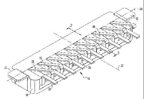
FIGS. 1-4 illustrate an electrical connector 10. With reference to FIG. 2, the
electrical connector 10 enables an electrical connection between a conductive
portion of a
device 12 such as a LCD and conductive elements 14 of a printed circuit board
16 having
an aperture 18 formed therein. The electrical connector 10 has a housing 20. A
first axis
22 can be said to extend along a first direction with respect to the housing
20. A second
axis 24 can be said to extend along a second direction with respect to the
housing 20. As
can be seen, the first axis 22 intersects the second axis 24 and the axes 22,
24 are generally
perpendicular to each other. The housing 20 is structured to be supportable
within the
aperture 18 of the printed circuit board 16. The electrical connector 10 is
shown
connected on an edge 26 of the printed circuit board 14.
One or more electrical contacts 28 are disposed on the housing 20. At least
some
of the electrical contacts 28 each have a connectable portion 30 extending
outwardly from
the housing 18 in a direction generally parallel with the first axis 22. The
connectable
portion 30 is structured to be connected to the conductive elements 14 of the
printed
circuit board 16. The conductive elements 14 may be soldered to the printed
circuit board
16 via surface mount technology techniques or connected by other similar
connecting
mechanisms. Each electrical contact 28 is structured to be electrically
connected with the
device 12.
A number of projections 32 extend outwardly from the housing 18 in a direction
generally parallel with the second axis 24. The projections 32 are structured
to be coupled
to pads 34 provided on the printed circuit board 14. The projections 32 may be
opposed to
one another as well. The connectable portion 30 and the projections 32 each
have a
mounting surface lying generally in a common plane. The projections 32 may be
soldered
to the pads 34 via surface mount technology techniques or connected by other
similar
connecting mechanisms. The projections 32 could be made from a piece of metal
that
2

CA 02595103 2007-07-26
extends along an entire length of the housing 20 in a direction of the second
axis 24. The
metal could, for example, be inserted and molded into the housing 20.
Alternatively, the
projections 32 could be made from at least a number of pieces of metal that
extend along a
portion of the length or the entire length of the housing 20 in the direction
of the second
axis 24. This metal could, for example, be inserted and molded into the
housing 18 as
well. As can be appreciated, other approaches exist for securing metal that
forms
projections 32 to the housing 18. By way of example and not of limitation, the
metal
could be connected to the housing 20 by snap fitting the metal into one or
more channels
(not shown) formed within the housing 20. While two projections 32 are shown
in the
FIGS., one would appreciate that any number of projections 32 could be used in
the
disclosed and claimed concepts of the patent application and the disclosure in
the FIGS.
should not be considered limiting.
Each electrical contact 28 may include a deflectable portion 36 to be
electrically
connected to the device 12. Each electrical contact 28 may also include an
arcuate tip 38.
Each electrical contact 28 is located in the housing 18 in spaced relation to
the other
electrical contacts 28. Generally speaking, each electrical contact 28 is
spaced in an
equidistant relationship from an adjacent electrical contact 28 of the
electrical connector
10. While each electrical contact 28 is shown in the FIGS. in a spaced
equidistant
relationship from an adjacent electrical contact 28, one would appreciate that
the electrical
contacts 28 do not necessarily have to be provided in a spaced equidistant
relationship
from an adjacent electrical contact 28 and that each electrical contact 28
could be provided
in a spaced non-equidistant relationship from an adjacent electrical contact
28, and the
disclosed and claimed concepts of the patent application and the disclosure in
the FIGS.
should not be considered limiting.
Each deflectable portion 36 is biased and extends outwardly from the housing
18
and is structured to be electrically connected with the device 12. The biased
deflectable
portion 36 may also have an arcuate tip 38 as well. The biased deflectable
portion 36 is
biased toward the device 12 electrically connected thereto. The biased
deflectable portion
36 also overlies at least a portion of the connectable portion 30.
Each electrical contact 28 may also have a housing portion 40 disposed on the
housing 18 which extends between the connectable portion 30 and the
deflectable portion
36. A portion 42 of the housing portion 40 may be received within a number of
apertures
44 formed within the housing 18. The portion 42 of the housing portion 40 may
be
3

CA 02595103 2007-07-26
secured to the housing 18 by placing or snapping barbs 46 within suitably
structured
recesses 48 proximate to the apertures 44. As can be seen in FIG. 5, the barb
46 has a first
edge 50 adjacent to a radius 52 that connects the housing portion 40 to the
connectable
portion 30. The first edge 50 extends outwardly in a direction generally
perpendicular to
the first axis 22 and has opposite ends 54. The opposite ends 54 of the first
edge 50 have a
second edge 56 attached to one of the opposite ends 54. The second edges 56
are located
in opposed relationship to each other and extend outwardly from one of the
opposite ends
54 in a general direction of the first axis 22. At a terminus 58 of the second
edges 56, the
second edges 56 are connected to a tapered portion 60 which gradually tapers
and ends at
a third edge 62 which extends in a general direction of the first axis 20. An
axis 64 which
extends along the second edge 56 forms an angle, 01 with an axis 66 that
extends along the
tapered portion 60. 01 may have a value of approximately 5 degrees to
approximately 85
degrees. It should be noted that 01 may have a value of anywhere between about
5 degrees
to about 85 degrees and other ranges falling within that range.
As can be seen in FIG. 2, the connectable portion 30 and the projections 32
are
structured to lie substantially flush with a surface of the printed circuit
board 16. At least
a portion of the electrical connector 10 is structured to be surface mounted
to the printed
circuit board 16. The projections 32 support the electrical connector 10
within the
aperture 18 of the printed circuit board 16. Such an approach minimizes the
overall
thickness of a product containing the electrical connector 10. By way of
example and not
of limitation, such products may be handheld electronic devices, television
sets,
camcorders, computer monitors, audio/visual equipment, car navigation systems,
gaming
devices and the like. The industry is continuously striving to reduce the
overall
thicknesses of a variety of electronic devices.
As can be seen in FIG. 6, a small amount of optional cushion material 68
having a
thickness of approximately 0.0 12 inch (0.3 mm) may be interposed between the
device 12
such as a LCD and the electrical connector 10. The deflectable portion 36 and
the
connectable portion 30 are in a spaced relationship from one another to define
a gap 70
therebetween to accommodate the optional amount of cushion material 68 used
between
the device 12 and the printed circuit board 16, if any. As can be appreciated,
the electrical
connector 10 may be constructed to provide any amount of preselected gap 70
between the
deflectable portion 36 and the connectable portion 30.
4

CA 02595103 2007-07-26
While specific embodiments of the disclosed and claimed concepts have been
described in detail, it will be appreciated by those skilled in the art that
various
modifications and alternatives to those details could be developed in light of
the overall
teachings of the disclosure. Accordingly, the particular arrangements
disclosed are meant
to be illustrative only and not limiting as to the scope of the disclosed and
claimed
concepts which is to be given the full breadth of the claims appended and any
and all
equivalents thereof.

Dessin représentatif
Une figure unique qui représente un dessin illustrant l'invention.
États administratifs

2024-08-01 : Dans le cadre de la transition vers les Brevets de nouvelle génération (BNG), la base de données sur les brevets canadiens (BDBC) contient désormais un Historique d'événement plus détaillé, qui reproduit le Journal des événements de notre nouvelle solution interne.

Veuillez noter que les événements débutant par « Inactive : » se réfèrent à des événements qui ne sont plus utilisés dans notre nouvelle solution interne.

Pour une meilleure compréhension de l'état de la demande ou brevet qui figure sur cette page, la rubrique Mise en garde , et les descriptions de Brevet , Historique d'événement , Taxes périodiques et Historique des paiements devraient être consultées.

Historique d'événement

Description Date
Exigences relatives à la révocation de la nomination d'un agent - jugée conforme 2023-11-11
Le délai pour l'annulation est expiré 2016-07-26
Lettre envoyée 2015-07-27
Accordé par délivrance 2011-11-22
Inactive : Page couverture publiée 2011-11-21
Inactive : Taxe finale reçue 2011-09-07
Préoctroi 2011-09-07
Inactive : CIB désactivée 2011-07-29
Un avis d'acceptation est envoyé 2011-07-26
Lettre envoyée 2011-07-26
Un avis d'acceptation est envoyé 2011-07-26
Inactive : Approuvée aux fins d'acceptation (AFA) 2011-07-20
Modification reçue - modification volontaire 2011-05-18
Inactive : CIB attribuée 2011-05-12
Inactive : CIB en 1re position 2011-05-12
Inactive : CIB attribuée 2011-05-12
Inactive : Dem. de l'examinateur par.30(2) Règles 2011-01-26
Inactive : CIB expirée 2011-01-01
Modification reçue - modification volontaire 2010-09-08
Inactive : Lettre officielle 2010-04-21
Exigences relatives à la révocation de la nomination d'un agent - jugée conforme 2010-04-21
Demande visant la révocation de la nomination d'un agent 2010-04-06
Inactive : Dem. de l'examinateur par.30(2) Règles 2010-03-11
Modification reçue - modification volontaire 2009-11-19
Inactive : Dem. de l'examinateur par.30(2) Règles 2009-05-19
Demande publiée (accessible au public) 2008-01-27
Inactive : Page couverture publiée 2008-01-27
Inactive : CIB attribuée 2007-12-21
Inactive : CIB attribuée 2007-12-20
Inactive : CIB en 1re position 2007-12-20
Inactive : CIB attribuée 2007-12-20
Inactive : Certificat de dépôt - RE (Anglais) 2007-08-23
Lettre envoyée 2007-08-23
Demande reçue - nationale ordinaire 2007-08-23
Toutes les exigences pour l'examen - jugée conforme 2007-07-26
Exigences pour une requête d'examen - jugée conforme 2007-07-26

Historique d'abandonnement

Il n'y a pas d'historique d'abandonnement

Taxes périodiques

Le dernier paiement a été reçu le 2011-06-13

Avis : Si le paiement en totalité n'a pas été reçu au plus tard à la date indiquée, une taxe supplémentaire peut être imposée, soit une des taxes suivantes :

  • taxe de rétablissement ;
  • taxe pour paiement en souffrance ; ou
  • taxe additionnelle pour le renversement d'une péremption réputée.

Les taxes sur les brevets sont ajustées au 1er janvier de chaque année. Les montants ci-dessus sont les montants actuels s'ils sont reçus au plus tard le 31 décembre de l'année en cours.
Veuillez vous référer à la page web des taxes sur les brevets de l'OPIC pour voir tous les montants actuels des taxes.

Historique des taxes

Type de taxes Anniversaire Échéance Date payée
Taxe pour le dépôt - générale 2007-07-26
Requête d'examen - générale 2007-07-26
TM (demande, 2e anniv.) - générale 02 2009-07-27 2009-06-16
TM (demande, 3e anniv.) - générale 03 2010-07-26 2010-06-22
TM (demande, 4e anniv.) - générale 04 2011-07-26 2011-06-13
Taxe finale - générale 2011-09-07
TM (brevet, 5e anniv.) - générale 2012-07-26 2012-06-14
TM (brevet, 6e anniv.) - générale 2013-07-26 2013-06-12
TM (brevet, 7e anniv.) - générale 2014-07-28 2014-07-21
Titulaires au dossier

Les titulaires actuels et antérieures au dossier sont affichés en ordre alphabétique.

Titulaires actuels au dossier
RESEARCH IN MOTION LIMITED
Titulaires antérieures au dossier
CHAO CHEN
Les propriétaires antérieurs qui ne figurent pas dans la liste des « Propriétaires au dossier » apparaîtront dans d'autres documents au dossier.
Documents

Pour visionner les fichiers sélectionnés, entrer le code reCAPTCHA :


Pour visualiser une image, cliquer sur un lien dans la colonne description du document (Temporairement non-disponible). Pour télécharger l'image (les images), cliquer l'une ou plusieurs cases à cocher dans la première colonne et ensuite cliquer sur le bouton "Télécharger sélection en format PDF (archive Zip)" ou le bouton "Télécharger sélection (en un fichier PDF fusionné)".

Liste des documents de brevet publiés et non publiés sur la BDBC .

Si vous avez des difficultés à accéder au contenu, veuillez communiquer avec le Centre de services à la clientèle au 1-866-997-1936, ou envoyer un courriel au Centre de service à la clientèle de l'OPIC.

({010=Tous les documents, 020=Au moment du dépôt, 030=Au moment de la mise à la disponibilité du public, 040=À la délivrance, 050=Examen, 060=Correspondance reçue, 070=Divers, 080=Correspondance envoyée, 090=Paiement})


Description du
Document 
Date
(aaaa-mm-jj) 
Nombre de pages   Taille de l'image (Ko) 
Abrégé 2007-07-25 1 19
Description 2007-07-25 5 235
Revendications 2007-07-25 6 223
Dessins 2007-07-25 5 91
Dessin représentatif 2008-01-01 1 16
Revendications 2009-11-18 6 226
Revendications 2010-09-07 6 237
Description 2010-09-07 7 343
Description 2011-05-17 7 343
Revendications 2011-05-17 6 238
Dessin représentatif 2011-10-17 1 18
Accusé de réception de la requête d'examen 2007-08-22 1 177
Certificat de dépôt (anglais) 2007-08-22 1 158
Rappel de taxe de maintien due 2009-03-29 1 112
Avis du commissaire - Demande jugée acceptable 2011-07-25 1 163
Avis concernant la taxe de maintien 2015-09-07 1 170
Correspondance 2010-04-05 3 197
Correspondance 2010-04-20 1 14
Correspondance 2010-04-20 1 21
Taxes 2010-06-21 1 35
Correspondance 2011-09-06 1 50