Note : Les descriptions sont présentées dans la langue officielle dans laquelle elles ont été soumises.
CA 02596751 2013-10-11
,
,
MULTIPLE-CORE PLANAR OPTICAL WAVEGUIDES AND
METHODS OF FABRICATION AND USE THEREOF
Applicant: Xponent Photonics Inc.
Inventors: Henry A. Blauvelt and David W. Vernooy
PRIORITY CLAIMS TO RELATED APPLICATIONS
[0001] This application claims priority based on U.S. non-provisional App. No.
11/058,535 filed 02/15/2005.
1
CA 02596751 2013-10-11
BACKGROUND
[0002] The field of the present invention relates to optical waveguides. In
particular,
multiple-core planar optical waveguides are disclosed herein, as well as
methods of
fabrication and use thereof.
[0003] Planar optical waveguides fabricated on waveguide substrates may be
incorporated into a variety of optical assemblies. Such optical waveguides may
be
fabricated with multiple cores or core layers. The use of such multiple-core
planar
optical waveguides may be advantageous in a variety of ways, as set forth
hereinbelow.
[0004] Subject matter disclosed in this application may be related to subject
matter
disclosed in: i) U.S. non-provisional App. No. 10/836,641 filed 04/29/2004
(U.S. Pat.
App. Pub. No. 2004/0264905 A1 published 12/30/2004); ii) U.S. non-provisional
App.
No. 10/682,768 filed 10/09/2003 (U.S. Pat. App. Pub. No. 2005/0078913 A1
published 04/14/2005); iii) U.S. non-provisional App. No. 10/661,709 filed
09/12/2003
(U.S. Pat. App. Pub. No. 2004/0129935 A1 published 07/08/2004); and iv) U.S.
non-
provisional App. No. 10/609,018 filed 06/27/2003 (U.S. Pat. App. Pub. No.
2004/0052467 A1 published 03/18/2004).
2
CA 02596751 2007-07-31
WO 2006/088872
PCT/US2006/005176
SUMMARY
[0005] A multiple-core optical waveguide comprises: a substantially planar
waveguide substrate; a lower waveguide core layer; an upper waveguide core
layer; a waveguide core between the upper and lower waveguide core layers;
lower
cladding between the substrate and the lower waveguide core layer; upper
cladding
above the upper waveguide core layer; and middle cladding between the upper
and
lower waveguide core layers substantially surrounding the waveguide core. Each
of the lower, middle, and upper claddings has a refractive index less than
refractive
indices of the lower waveguide core layer, the upper waveguide core layer, and
the
waveguide core. Along at least a given portion of the optical waveguide, the
upper
and lower waveguide core layers extend bilaterally substantially beyond the
lateral
extent of a propagating optical mode supported by the optical waveguide, the
lateral extent of the supported optical mode being determined at least in part
by the
width of the waveguide core along the given portion of the optical waveguide.
The
optical waveguide may further comprise a second waveguide core. The waveguide
cores may taper in various ways so as to effect mode conversions by optical
coupling between the waveguide cores. The waveguide may terminate at an end
face thereof for optical end-coupling with an optical fiber or with a planar
waveguide, and a terminal segment of the waveguide may be adapted for such
end-coupling.
[0006] The waveguide may be fabricated by: forming a lower cladding layer on a
waveguide substrate; forming a lower waveguide core layer on the lower
cladding
layer; forming a lower portion of a middle cladding layer on the lower core
layer;
forming a waveguide core on the lower portion of the middle cladding layer;
forming
an upper portion of the middle cladding layer over the waveguide core and on
exposed areas of the lower portion of the middle cladding layer; forming an
upper
waveguide core layer on the upper portion of the middle cladding layer; and
forming
an upper cladding layer on the upper waveguide core layer. Spatial patterning
of
various waveguide cores, core layers, or claddings may be done sequentially or
concurrently.
3
CA 02596751 2013-10-11
[0006a] According to one embodiment, there is provided a planar optical
waveguide
comprising: a substantially planar waveguide substrate; lower cladding formed
on the
waveguide substrate; a lower waveguide core layer formed on the lower
cladding;
middle cladding formed on the lower waveguide core layer; an upper waveguide
core
layer formed on the middle cladding; upper cladding formed on the upper
waveguide
core layer; and a first waveguide core between the upper and lower waveguide
core
layers that is separated from the upper and lower waveguide core layers by
portions
of the middle cladding and that defines an optical waveguide propagation path.
A
width of the first waveguide core is substantially larger than a thickness of
the first
waveguide core, and the first waveguide core has a substantially flat upper
surface.
Each one of the lower cladding, the middle cladding, and the upper cladding
has a
corresponding refractive index that is less than a corresponding refractive
index of
any of the lower waveguide core layer, the upper waveguide core layer, and the
first
waveguide core. Along a first segment of the propagation path: the width of
the first
waveguide core is substantially constant; the upper and lower waveguide core
layers
and the first waveguide core are arranged so as to together form an optical
waveguide that guides a first optical mode propagating along the first segment
of the
propagation path; the upper and lower waveguide core layers extend bilaterally
substantially beyond a lateral extent of the first optical mode; and the upper
and lower
waveguide core layers and the first waveguide core are arranged so that the
first
optical mode is guided bilaterally by the first waveguide core, from below by
the lower
waveguide core layer, and from above by the upper waveguide core layer.
[0007] Aspects and advantages pertaining to multiple-core planar optical
waveguides as disclosed herein may become apparent upon referring to the
disclosed exemplary embodiments as illustrated in the drawings and disclosed
in the
following written description or claims.
4
CA 02596751 2007-07-31
WO 2006/088872
PCT/US2006/005176
BRIEF DESCRIPTION OF THE DRAWINGS
[0008] Figs. 1A-1E are cross-sectional views of exemplary multiple-core
optical
waveguides.
[0009] Figs. 2A-2E are cross-sectional views of an exemplary multiple-core
optical
waveguides.
[0010] Figs. 3A-3E are plan and cross-sectional views of an exemplary multiple-
core optical waveguide.
[0011] Figs. 4A-4D are plan and cross-sectional views of an exemplary multiple-
core optical waveguide.
[0012] The embodiments shown in the Figures are exemplary, and should not be
construed as limiting the scope of the present disclosure and/or appended
claims. It should be noted that the relative sizes or proportions of
structures shown in the Figures may in some instances be distorted to
facilitate illustration of the disclosed embodiments.
5
CA 02596751 2007-07-31
WO 2006/088872
PCT/US2006/005176
DETAILED DESCRIPTION OF EMBODIMENTS
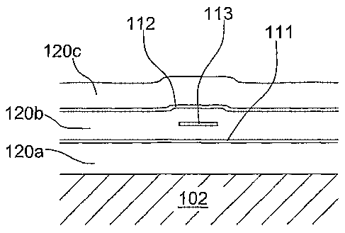
[0013] Exemplary embodiments of a multiple-core low-contrast planar waveguide
are shown in cross-section in Figs. 1A-1E positioned on a waveguide substrate
102. Substrate 102 may comprise a semiconductor substrate such as silicon in
this
example, although any suitable substrate material may be employed. In this
example, low-contrast waveguide core 113 comprises doped silica and is
surrounded by lower-index middle cladding layer 120b, which comprises doped or
undoped silica with a refractive index between about 1.44 and 1.46. The terms
"low-contrast" or "low-index-contrast" as used herein shall denote index
contrast
less than about 5%. The index contrast between waveguide core 113 and middle
cladding 120b in this example is less than about 5%, or may be between about
0.5% and about 3%, or may be between about 1% and about 2%. For example,
core 113 may have an index typically between about 1.46 and about 1.48. Middle
cladding layer 120b and core 113 therein are disposed between two doped silica
core layers 111 and 112, which are in turn disposed between lower-index upper
cladding 120c and lower-index lower cladding 120a. Cladding layers 120a and
120c in this example comprise doped or undoped silica with refractive indices
similar to or the same as middle cladding 120b. Core layers 111 and 112 may
comprise doped silica, with refractive indices larger than those of the
cladding
layers 120a, 120b, and 120c, and similar to or the same as the refractive
index of
waveguide core 113. Any other suitable materials may be employed for forming
core 113, core layers 111 and 112, or claddings 120a, 120b, or 120c.
[0014] In the examples of Figs. 1B and 1E, the core layers 111 and 112 extend
bilaterally substantially beyond the transverse extent of a propagating
optical mode
supported by the waveguide. Such an optical mode is typically confined
laterally by
the waveguide core 113, and the transverse extent of core 113 at least in part
determines the transverse extent of the supported optical mode. In the
examples
of Figs. 1A, 1C, and 1D, claddings layers 120a, 120b, or 120c may be formed so
as
to yield a protruding lateral surface terminating core layer(s) 111 and/or
112. Such
lateral surfaces may be provided at varying depths, and may or may not extend
downward near or beyond the depth of core 113. A waveguide may be formed to
include multiple segments having various of the configurations shown in Fig.
1A-1E.
In some embodiments having one or two lateral protruding surfaces, core layers
6
CA 02596751 2007-07-31
WO 2006/088872
PCT/US2006/005176
111 and 112 may extend bilaterally substantially beyond the transverse extent
of a
supported optical mode. Alternatively, in other embodiments the transverse
extent
of a supported optical mode may be in part determined by the transverse extent
of
the core layers 111 and 112 (if they terminate sufficiently close to waveguide
core
113), or by the presence of the lateral protruding surface (if it is formed
sufficiently
close to waveguide core 113). In all of the exemplary multiple-core low-
contrast
waveguides of Figs. 1A-1E, a supported propagating optical mode is
substantially
confined vertically by core layers 111 and 112, while the presence of core 113
influences the details of the spatial mode profile (along the vertical
dimension) near
its center.
[0015] In an exemplary multiple-core low-contrast waveguide with silica or
doped
silica core, core layers, and claddings as described above, waveguide core 113
may be about 0.7 m thick by about 8 !Am wide, core layers 111 and 112 may
each
be about 0.6 m thick, and the thickness of middle cladding 1120b separating
core
113 from each of the core layers 111 and 112 may be about 1.5 p.m. At a
wavelength of about 1.3-1.5 m, these dimensions may yield a transverse mode
size of around 8 m high by around 10 m wide (mode sizes expressed as 1/e2 HW
power). Other dimensions or indices for the core, core layers, or claddings
may be
chosen to yield suitable mode size and shape within the scope of the present
disclosure. A suitable mode size and shape may be chosen for spatial-mode
matching with an optical fiber mode or a mode of another optical waveguide,
for
example, thereby enabling end-coupling with reduced level of diffractive
optical
loss. Core 113 may range from about 0.3 m thick up to about 1 rn thick, and
between about 3 m wide and about 12 !Am wide. In some instances where single-
mode behavior is not required, core 113 may be as wide as about 15 m or about
20 m. Core layers 111 and 112 may range from about 0.3 m thick up to about 2
prn thick. Refractive indices for core 113 and core layers 111/112 typically
range
between about 1.46 and about 1.48, while that of the claddings 120a/120b/120c
typically range between about 1.44 and 1.46. Any other suitable indices may be
employed within one or more of the index-contrast ranges given above. The
portions of cladding 120b separating core 113 from core layers 111/112 may
range
between about 1 m thick and about 3 m thick. Specific combinations of
dimensions will depend on the desired spatial mode characteristics and the
7
CA 02596751 2007-07-31
WO 2006/088872
PCT/US2006/005176
particular degree of index contrast employed. In addition to doped and undoped
silica, other suitable core and cladding materials may be equivalently
employed. As
in the previous examples, lower cladding layer 120a below core layer 111 may
be
sufficiently thick so as to reduce or substantially eliminate optical leakage
from the
waveguide into substrate 102 (within operationally acceptable limits), or a
reflective
coating between the cladding and the substrate may be employed (as described
hereinabove). The lower cladding may be grater than about 5 pm thick, or
between
about 6 pm thick and about 12 pm thick or between about 8 j.im thick and about
10
m thick. Similarly, upper cladding layer 1120c above upper core layer 112 may
be
sufficiently thick so as to reduce or substantially eliminate optical leakage
through
the upper surface of the waveguide (within operationally acceptable limits) or
to
substantially isolate a supported optical mode from a use environment (within
operationally acceptable limits). The upper cladding may be greater than about
5
pm thick, or between about 6 p.m thick and about 12 p.m thick or between about
8
p.m thick and about 10 pm thick.
[0016] Fabrication of a multiple-core low-contrast waveguide, such as the
examples shown in Figs. 1A-1E, typically begins with deposition (in order) of
lower
cladding 120a, core layer 111, and a lower portion of cladding 120b. Waveguide
core 113 is then formed on the substantially planar upper surface of the
deposited
cladding 120b, typically by spatially-selective deposition or by substantially
uniform
deposition followed by spatially-selective removal. After forming core 113,
additional cladding 120b is deposited, which may or may not comprise the same
material as that deposited to form the lower portion of cladding 120b. If a
deposition process having a substantial degree of conformality is employed,
the
upper surface of cladding 120b may exhibit a raised portion directly above
waveguide core 113. Upper core layer 112 may be deposited directly on such a
non-planar cladding surface, resulting in a corresponding raised portion of
core
layer 112 directly over waveguide core 113. Upper cladding 120c may be
deposited on the non-planar core layer 112, resulting in a corresponding non-
planar
upper surface of cladding layer 120c. The multiple-core low-contrast waveguide
resulting from this exemplary fabrication sequence would resemble the
exemplary
embodiment shown in Fig. 1B. If a deposition process for cladding 120b is
employed that yields a substantially flat upper surface regardless of
underlying
8
CA 02596751 2007-07-31
WO 2006/088872
PCT/US2006/005176
topology, or if a non-planar upper surface of cladding 120b is substantially
planarized prior to deposition of core layer 112 thereon, then the resulting
multiple-
core waveguide would resemble the exemplary embodiment shown in Fig. 1E. In
either case (planar or non-planar core layer 112) the resulting waveguide may
be
further processed to yield protruding lateral surfaces as shown in Figs. 1A,
1C, or
1D, if needed or desired. For relatively low index contrast (less than about
5%, for
example), and sufficiently thin waveguide core 113 (less than about 1 pm, for
example), a multiple-core waveguide with a non-planar upper core layer 112
exhibits optical performance characteristics substantially similar to those
exhibited
by a multiple-core waveguide with a substantially planar upper core layer 112.
[0017] Exemplary multiple-core planar optical waveguides are shown in Figs. 2A-
2E that also include a high-contrast core. As in the preceding examples,
substrate
202 may comprise silicon, although any suitable substrate material(s) may be
employed, and cladding layers 220a, 220b, and 220c may comprise doped or
undoped silica of suitable thicknesses (index between about 1.44 and about
1.46),
although any suitable cladding material(s) may be employed. In this example, a
high-index-contrast waveguide core 213b may comprise a layer of silicon
nitride or
silicon oxynitride a few tens to a few hundreds of nanometers in thickness,
and
several microns in width (high-index-contrast, greater than about 5%). The
high-
contrast core 213b may extend along the entire waveguide, or may extend along
only one or more segments of the waveguide while being absent from other
segments. Low-index-contrast core 213a may comprise doped silica about 0.7 jm
thick and about 8 pm wide, with a refractive index in this example between
about
1.46 and about 1.48. Low-index-contrast core layers 211 and 212 may also
comprise silica or doped silica about 0.6 p.m thick, with refractive indices
similar to
or the same as waveguide core 213a. In the examples shown waveguide cores
213a and 213b are in contact; embodiments wherein cores 213a and 213b are
separated by cladding material 220b shall also fall within the scope of the
present
disclosure or appended claims. Over portions of the waveguide where waveguide
core 213b is present and waveguide core 213a is at least a few tens of microns
wide, or where waveguide core 213b is greater than 1 to 2 ,m wide, the
presence
of waveguide core 213a and core layers 211/212 may have little or no effect on
the
optical mode characteristics of the waveguide, which are substantially
determined
9
CA 02596751 2007-07-31
WO 2006/088872
PCT/US2006/005176
by the size, shape, and index-contrast on core 213b. Over waveguide segments
lacking waveguide core 213b, waveguide core 213a and core layers 211/212 may
support an optical mode with characteristics substantially determined by their
index
contrast, dimensions, and relative positions and the index of cladding layers
220a/220b/220c. As the size of waveguide core 213b decreases below about 1 to
2 microns in width until it is no longer present, an optical mode supported by
the
waveguide undergoes a continuous evolution between these two extremes, and
various desired mode sizes, shapes, or other characteristics may be achieved
by
appropriate combinations of dimensions for the waveguide cores 213a/213b and
layers 211/212. Lateral portions of claddings 220a/220b/220c and layers
211/212
may be configured in any of the various ways described hereinabove (i.e. with
or
without a protruding lateral surface), and the waveguide may be formed to
include
multiple segments having various of such configurations.
[0018] The multiple-core structure of the waveguide of Figs. 2A-2E enables a
wide
array of optical designs for achieving various optical performance and/or
functionality. As described hereinabove, the high-index-contrast core layer
213b
may be readily adapted for substantially spatial-mode-matched optical end
coupling
with another optical waveguide or semiconductor optical device, or for optical
transverse-coupling with another optical waveguide (substantially adiabatic,
substantially modal-index-matched, or otherwise), for illuminating a
photodetector,
or for other purposes. The low-index-contrast core 213a and core layers
211/212
may be readily adapted for substantially spatial-mode-matched optical end-
coupling
with another optical waveguide or with an optical fiber, or for enabling
insertion of
various free-space optical components between the ends of two such optical
waveguides, or for other purposes. Such adaptations of waveguide core 213a and
core layers 211/212 may include the presence of waveguide core 213b at a
reduced width (less than about 1 pm wide, for example) to achieve the desired
mode characteristics. Substantially adiabatic transitions may be made between
these two distinct waveguide types (high-index-contrast core and low-index-
contrast multiple-core) by spatially selective patterning of materials forming
waveguide cores 213a and 213b.
[0019] As shown in Figs. 3A-3E, a high-index-contrast waveguide core 313b a
few
microns wide may be patterned between substantially uniform low-index-contrast
CA 02596751 2007-07-31
WO 2006/088872
PCT/US2006/005176
core layers 311/312 and substantially uniform waveguide core material layer
313a
over a first segment 300a of a waveguide. Along this first waveguide segment
300a, the high-contrast waveguide core 313b substantially determines the
characteristics of a guided optical mode, while layers 311/312/313a have
negligible
influence on the properties of the waveguide (Fig. 3B). Along a second
waveguide
segment 300b, waveguide core material layer 313a may be patterned as well as
waveguide core 313b. Layer 313b may be patterned to continue the presence of
the high-index-contrast core, while layer 313a may be patterned to form the
low-
index-contrast waveguide core (Fig. 30). The patterning of layer 313a may be
such
that the low-index-contrast waveguide core appears gradually (i.e.,
substantially
adiabatically, as shown), or the low-index-contrast core may appear abruptly
(not
shown). High-contrast core 313b continues to substantially determine the
optical
characteristics of the waveguide along segment 300b. Along a third segment
300c
of the waveguide (Fig. 3D), high-contrast waveguide core 313b is patterned so
as
to gradually decrease in width along the length of the waveguide until it
finally
terminates, while low-contrast waveguide core 313a continues to be present
along
the length of segment 300c. This tapering of high-contrast waveguide core 313b
is
sufficiently gradual so as to allow a substantially adiabatic transition
between a
waveguide optical mode characteristic of high-contrast waveguide core 313b at
one
end of segment 300c to a waveguide optical mode characteristic of low-contrast
waveguide core 313a and core layers 311/312 at the other end of segment 300c.
A
fourth segment 300d of the waveguide includes only low-contrast waveguide core
313a and core layers 311/312, without high-contrast waveguide core 313b (Fig.
3E). Instead of terminating, high-contrast waveguide core 313b may taper to
some
minimum width (less than about 1 jam, for example; not shown) and then remain
at
that width along segment 300d, in order to achieve desired characteristics for
an
optical mode supported by segment 300d. The exemplary optical waveguide
shown in Figs. 3A-3E may serve as an optical mode converter, with optical
power
propagating in either direction.
[0020] In variants of the multiple-core embodiments of Figs. 2A-2E and 3A-3E,
the
high-contrast core 213b/313b may be positioned at any suitable vertical
position
relative to the low-contrast core layers 211/311 and 212/312 and the low-
contrast
core 313a. Positioning of the high-contrast core 213b/313b at one of the low-
11
CA 02596751 2007-07-31
WO 2006/088872
PCT/US2006/005176
contrast layer interfaces may reduce the number of fabrication steps (by
eliminating
the need to deposit a layer surrounding core 213b/313b in two steps).
Placement
of high-contrast core 213b/313b in contact with low-contrast core 213a/313a
between core layers 211/311 and 212/312 may result in preferential optical
coupling into the lowest-order symmetric mode supported by the multiple-core
low-
contrasts waveguide. Instead of the substantially adiabatic transitions
between
core high-contrast core 313b and low-contrast core 313a (Figs. 3A-3E), in
other
various embodiments cores 313a and 313b may appear and/or terminate abruptly
instead of gradually. Such an arrangement may be appropriate for substantially
modal-index-matched optical transverse-coupling between the cores, instead of
substantially adiabatic transverse-coupling. Many other variants of these
embodiments may be contemplated within the scope of the present disclosure.
[0021] The exemplary waveguides of Figs. 2A-2E and 3A-3E may be fabricated by
processing sequences similar to that described hereinabove for the fabrication
of
the exemplary waveguides of Figs. 1A-1E. Fabrication of a waveguide, such as
the
examples shown in 2A-2E for example, may typically begin with deposition (in
order) of lower cladding 220a, core layer 211, and a lower portion of cladding
220b.
Cores 213a and 213b may then be formed on the substantially planar upper
surface of the deposited cladding 220b, typically by spatially-selective
deposition or
by substantially uniform deposition followed by spatially-selective removal.
If the
latter, both material layers may be deposited before either is spatially-
selectively
processed. If cores 213a and 213b are to be separated by cladding 220b, an
intermediate layer of cladding 220b would be deposited after forming one core
and
before forming the other (with or without planarizing the upper surface of
this
intermediate cladding layer, as discussed hereinabove). After cores 213a and
213b
are formed, additional cladding 220b is deposited, which may or may not
comprise
the same material as that deposited to form the lower portion of cladding 220b
(or
the intermediate portion, if any). If a deposition process having a
substantial
degree of conformality is employed, the upper surface of cladding 220b may
exhibit
a raised portion directly above waveguide cores 213a and 213b. Upper core
layer
212 may be deposited directly on such a non-planar cladding surface, resulting
in a
corresponding raised portion of core layer 212 directly over waveguide cores
213a
and 213b. Upper cladding 220c may be deposited on the non-planar core layer
12
CA 02596751 2007-07-31
WO 2006/088872
PCT/US2006/005176
212, resulting in a corresponding non-planar upper surface of cladding layer
1220c.
The multiple-core waveguide resulting from this exemplary fabrication sequence
would resemble the exemplary embodiment shown in Fig. 2B. If a deposition
process for cladding 220b is employed that yields a substantially flat upper
surface
regardless of underlying topology, or if a non-planar upper surface of
cladding 220b
is substantially planarized prior to deposition of core layer 212 thereon,
then the
resulting multiple-core waveguide would resemble the exemplary embodiment
shown in Fig. 2E. In either case (planar or non-planar core layer 212) the
resulting
waveguide may be further processed to yield protruding lateral surfaces as
shown
in Figs. 2A, 2C, or 2D, if needed or desired. For relatively low index
contrast (less
than about 5%), and sufficiently thin waveguide core 213 (less than about 1
lam, for
example), a multiple-core waveguide with a non-planar upper core layer 212
exhibits optical performance characteristics substantially similar to those
exhibited
by a multiple-core waveguide with a substantially planar upper core layer 212.
[0022] In the exemplary embodiment of Figs. 4A-4D, a multiple-core waveguide
formed on substrate 402 terminates at a V-groove 403 formed on segment 400c of
the substrate. An optical fiber (not shown) received in V-groove 403 may be
end-
coupled to the waveguide. An optical mode supported by segment 400a of the
waveguide may exhibit a somewhat elliptical transverse mode shape elongated in
the horizontal dimension. While such a mode might be adequate for end-coupling
to another similarly configured waveguide, it might provide less-than-optimal
end-
coupling to the optical fiber received in groove 403. Terminal segment 400b of
the
waveguide may be adapted for supporting a more nearly symmetric spatial mode
at
the end face thereof, thereby enhancing end-coupling to an optical fiber
received in
V-groove 403. One suitable adaptation is shown in Figs. 4A-4D, where two areas
adjacent segment 400b of the waveguide are etched (or otherwise processed) so
as to remove core and cladding materials down to the substrateb402 and to form
lateral protruding surfaces 404. The etched areas are arranged so that near
the
end of the waveguide, core layers 411 and 412 terminate near enough to the
lateral
edges of waveguide core 413 so that layers 411 and 412 at least in part
laterally
confine the propagating optical mode. By choosing a suitable width for layers
411
and 412 at the end of the waveguide (the choice based in part on the
refractive
index of any material, such as an embedding medium or encapsulant, that might
be
13
CA 02596751 2007-07-31
WO 2006/088872
PCT/US2006/005176
employed subsequently to fill the etched areas), the shape of the propagating
mode
may be made to better match that of an optical fiber, so as to provide end-
coupling
between the waveguide and fiber at or above an operationally acceptable level.
The transition between waveguide segment 400a and the end of waveguide
segment 400b may be made substantially adiabatic, if needed or desired, with
core
layers 411 and 412 tapering in width along the waveguide toward the waveguide
end face. It is often the case that an index matching substance is deposited
between the end of the waveguide and the optical fiber, and such index-
matching
material may be employed to fill the etched areas as well, provided its
refractive
index is less than the refractive index of the core layers 411 and 412, or no
greater
than the refractive index of cladding layers 420a, 420b, or 420c. For ease of
processing, in some embodiments a thin end wall 405 may be left at the very
end of
the waveguide; the wall would include layers 420a/420b/420c and 411/412. Such
an end wall may be made sufficiently thin (less than about 10 m, typically
only 2-3
pm) so as not to substantially influence the propagating optical mode entering
or
exiting the end face of the waveguide. Embodiments with or without an end wall
shall fall within the scope of the present disclosure or appended claims.
[0023] Instead of etching both core layers 411/412 and all claddings
420a/420b/420c in a single step so that core layers 411/412 at least partly
laterally
confine the propagating optical mode (resulting in a structure such as that of
Figs.
4A-4D, for example), core layers 411/412 may be individually patterned during
fabrication of the waveguide so as to taper in width along the waveguide
toward the
waveguide end face (not shown). As a result of such a fabrication scheme,
middle
cladding 420b would come into contact with the lateral edges of core layer
411,
while upper cladding 420c would come into contact with the lateral edges of
core
layer 412.
[0024] For the typical dimensions and index contrast disclosed hereinabove for
exemplary waveguides, it has been observed that the lower and upper core
layers
411/412 contribute to lateral confinement at the waveguide end face if they
terminate less than about 15 pm from the respective lateral edges of the core
413.
Wider core layers 411/412 at the end face do not appear to provide a
substantially
degree of confinement. The widths of the terminated core layers 411/412 near
the
waveguide end face may range from about the width of core 413 up to about 30
m
14
CA 02596751 2007-07-31
WO 2006/088872
PCT/US2006/005176
greater than the width of core 413, or may range between about 6 pm wider and
about 20 p.m wider than core 413, or may range between about 8 pm wider and
about 12 p.m wider than core 413.
[0025] Instead of a V-groove for receiving an optical fiber for end-coupling,
substrate 402 have a second optical waveguide formed thereon and positioned
for
end-coupling (not shown). Alternatively, substrate 402 may be adapted for
receiving a second planar optical waveguide formed on a second substrate and
subsequently assembled with substrate 402 for end-coupling (not shown). In
either
of these alternative scenarios, the terminal segment 400b of the waveguide may
be
adapted in any suitable fashion for enabling end-coupling between the
waveguides
at or above an operationally acceptable level.
[0026] The exemplary embodiments of multiple-core waveguides shown in Figs.
1A-1E, 2A-2E, 3A-3B, and 4A-4D, and variants thereof, exhibit many of the
desirable optical properties exhibited by dual-core waveguides disclosed in
earlier-
cited App. No. 10/836,641. Adjustment of the index or thickness of the core,
core
layers, or cladding layers allows adjustment of spatial properties of the
propagating
optical modes supported by the multiple-core waveguide. The multiple-core
waveguide enables efficient end-coupling with other optical waveguides,
including
other planar optical waveguides and optical fibers. The transverse dimensions
of
an optical mode supported by the multiple-core waveguide are typically
substantially invariant with wavelength (at least over the range of typical
near-
infrared telecommunications wavelengths). The lowest order mode supported by
the multiple-core waveguide may be substantially spatial-mode-matched with
another planar waveguide, or with an optical fiber (particularly if adapted as
in Figs.
4A-4D). An optical mode supported by the multiple-core waveguide tends to
exhibit
a minimum phase front curvature upon propagating some distance beyond an end
face of the waveguide. Such a minimum phase fronts tend to occur about 5 to 30
p.m away from a waveguide end face, for the typical wavelengths and mode sizes
discussed herein. This enables substantial reduction in diffractive optical
losses
upon end coupling with another planar waveguide or with an optical fiber.
Multiple-
core low-contrast waveguides may be advantageously implemented where free-
space optical propagation between waveguides is required, for example
according
to the teachings of earlier-cited App. No. 10/682,768. Multiple-core low-
contrast
CA 02596751 2007-07-31
WO 2006/088872
PCT/US2006/005176
waveguides may be advantageously implemented where free-space optical
propagation from the end face of the waveguide to a photodetector is required,
for
example according to the teachings of earlier-cited App. No. 10/661,709.
Multiple-
core low-contrast waveguides may also exhibit reduced polarization and/or
wavelength dependences relative to single-core planar waveguides. While
remaining within the scope of the present disclosure and/or appended claims,
the
indices, thicknesses, and transverse dimensions for the core, core layers, and
cladding layers of any of the waveguides of Figs. 1A-1E, 2A-2E, 3A-3E, and 4A-
4D
may all be optimized to achieve desired operationally acceptable performance
(with
respect to optical loss, polarization dependence, wavelength dependence,
spatial
mode matching, and so forth).
[0027] The exemplary low-profile-core waveguides shown in the Figures
represent
only a sampling of various embodiments of planar waveguides that may be formed
with one or more low-profile core(s) or core layers. While exemplary
embodiments
are shown that include one, two, three, or four waveguide cores or core
layers,
embodiments including still larger numbers of waveguide cores may be
implemented within the scope of the present disclosure. Many other suitable
low-
profile-core waveguide configurations may be employed, and other suitable
materials and/or material combinations used therefor, while remaining within
the.
scope of the present disclosure.
[0028] A low-contrast multiple-core waveguide as disclosed herein may exhibit
relatively little or substantially negligible polarization or wavelength
dependence.
Such waveguides may be well-suited for applications where such dependencies
may be undesirable or unacceptable. For example, such a substantially
polarization-independent waveguide may be employed in an optical receiver in
which the polarization state of incoming light may not be known or may vary
over
time. Such low-contrast multiple-core waveguides may typically support modes
more suitable for applications involving free-space optical propagation
between
adjacent end faces of two waveguides (often through an intervening optical
component) than their high-contrast or single-core counterparts. The mode
characteristic of a low-contrast multiple-core waveguide may suffer relatively
less
diffractive optical loss upon transmission between the waveguide end faces.
16
CA 02596751 2007-07-31
WO 2006/088872
PCT/US2006/005176
[0029] As noted above, relative to single-core low-contrast waveguides (as in
earlier-cited App. No. 10/836,641), multiple-core low-contrast waveguides
disclosed
herein tend to exhibit modal characteristics that are less dependent or
negligibly
dependent on polarization or wavelength. In addition, for a given mode size
(expressed as 11e2 HW power) in the vertical dimension, an optical mode
supported
by a single-core low-contrast waveguide has exponentially decaying wings that
extend substantially farther from the mode axis than those of an optical mode
supported by a multiple-core low-contrast waveguide. As a result, for a given
upper
and lower cladding thickness, a multiple-core low-contrast waveguide exhibits
less
optical loss through coupling into the substrate or into the surroundings than
a
single-core low-contrast waveguide. Or, for a given operationally acceptable
level
of optical loss, thinner upper and lower cladding layers may be employed with
a
multiple-core low-contrast waveguide.
[0030] Multiple-core low-contrast waveguides offer the fabrication advantages
of
low-profile and thin cores (shallower etches, more precise lithography,
substantially
complete filling between etched features, substantially flat upper surfaces of
deposited layers, and so on; as disclosed in earlier-cited App. Nos.
10/609,018 and
10/836,641), while providing desirable optical properties characteristic of
thicker
single cores. For example, if the layers of Figs. 1A-1E are each deposited and
spatially patterned sequentially, then no layer thicker than about 1.0 pm (and
typically no thicker than about 0.7 [tm) need ever be spatially patterned. The
low-
profile of patterned core 113, for example, ensures that subsequent deposition
of a
portion of middle cladding 120b results in a substantially flat upper surface
for
deposition of core layer 112. A multiple-core low-contrast waveguide as in
Figs.
1A-1E exhibits many of the desirable optical characteristics of a thicker
single core,
but requires only a single patterning step of a layer typically less than
about 1 tim
thick, and often less than about 0.7 pm thick.
[0031] The term "optical waveguide" (or equivalently, "waveguide") as employed
herein shall denote a structure adapted for supporting one or more optical
modes.
Such waveguides shall typically provide confinement of a supported optical
mode in
two transverse dimensions while allowing propagation along a longitudinal
dimension. The transverse and longitudinal dimensions/directions shall be
defined
locally for a curved waveguide; the absolute orientations of the transverse
and
17
CA 02596751 2007-07-31
WO 2006/088872
PCT/US2006/005176
longitudinal dimensions may therefore vary along the length of a curvilinear
waveguide, for example. Examples of optical waveguides may include, without
being limited to, various types of optical fiber and various types of planar
waveguides. The term "planar optical waveguide" (or equivalently, "planar
waveguide") as employed herein shall denote any optical waveguide that is
provided on a substantially planar substrate. The longitudinal dimension
(i.e., the
propagation dimension) shall be considered substantially parallel to the
substrate.
A transverse dimension substantially parallel to the substrate may be referred
to as
a lateral or horizontal dimension, while a transverse dimension substantially
perpendicular to the substrate may be referred to as a vertical dimension.
Terms
such "above" and "below", "top" and "bottom", "up" and "down", and so forth
shall
be defined relative to the substrate, with the waveguide defined as "above"
the
substrate. Examples of such waveguides include ridge waveguides, buried
waveguides, semiconductor waveguides (silicon, silicon-based, III-V, others),
other
high-index waveguides ("high-index" being above about 2.5), silica-based
waveguides (silica, doped silica, and/or other silica-based materials),
polymer
waveguides, other low-index waveguides ("low-index" being below about 2.5),
core/clad type waveguides, multi-layer reflector (MLR) waveguides, metal-clad
waveguides, air-guided waveguides, vacuum-guided waveguides, photonic crystal-
based or photonic bandgap-based waveguides, waveguides incorporating electro-
optic (EO) and/or electro-absorptive (EA) materials, waveguides incorporating
non-
linear-optical (NLO) materials, and myriad other examples not explicitly set
forth
herein which may nevertheless fall within the scope of the present disclosure
and/or
appended claims. Many suitable substrate materials may be employed, including
semiconductor (silicon, silicon-based, III-V, others), crystalline, silica or
silica-
based, other glasses, ceramic, metal, and myriad other examples not explicitly
set
forth herein which may nevertheless fall within the scope of the present
disclosure
and/or appended claims. For purposes of the foregoing written description
and/or
the appended claims, "index" may denote the bulk refractive index of a
particular
material (also referred to herein as a "material index") or may denote an
"effective
index" neff, related to the propagation constant 13 of a particular optical
mode in a
particular optical element by 13 = 211NA. The effective index may also be
referred
18
CA 02596751 2007-07-31
WO 2006/088872
PCT/US2006/005176
to herein as a "modal index". "Low-contrast" or "low-index-contrast" shall
denote
materials having an index contrast less than about 5%, while "high-contrast"
or
"high-index-contrast" shall denote materials having an index contrast greater
than
about 5%.
[0032] One exemplary type of planar optical waveguide that may be suitable for
use with optical components disclosed herein is a so-called PLC waveguide
(Planar
Lightwave Circuit). Such waveguides typically comprise silica or silica-based
waveguides (often ridge or buried waveguides; other waveguide configuration
may
also be employed) supported on a substantially planar silicon substrate (often
with
an interposed silica or silica-based optical buffer layer). Sets of one or
more such
waveguides may be referred to as planar waveguide circuits, optical integrated
circuits, or opto-electronic integrated circuits. A PLC substrate with one or
more
PLC waveguides may be readily adapted for mounting one or more optical
sources,
lasers, modulators, and/or other optical devices adapted for end-transfer of
optical
power with a suitably adapted PLC waveguide. A PLC substrate with one or more
PLC waveguides may be readily adapted (according to the teachings of U.S.
Patent
Application Pub. Nos. 2003/0081902, 2004/0052467, or 2004/0264905, for
example) for mounting one or more optical sources, lasers, modulators,
photodetectors, and/or other optical devices adapted for transverse-transfer
of
optical power with a suitably adapted PLC waveguide (mode-interference-coupled
transverse-transfer or substantially adiabatic transverse-transfer; also
referred to as
transverse-coupling).
[0033] For purposes of the present written description or appended claims,
"spatially-selective material processing techniques" shall encompass epitaxy,
layer
growth, lithography, photolithography, evaporative deposition, sputtering,
vapor
deposition, chemical vapor deposition, beam deposition, beam-assisted
deposition,
ion beam deposition, ion-beam-assisted deposition, plasma-assisted deposition,
wet etching, dry etching, ion etching (including reactive ion etching), ion
milling,
laser machining, spin deposition, spray-on deposition, electrochemical plating
or
deposition, electroless plating, photo-resists, UV curing or densification,
micro-
machining using precision saws or other mechanical cutting/shaping tools,
selective
metallization or solder deposition, chemical-mechanical polishing for
planarizing,
19
CA 02596751 2007-07-31
WO 2006/088872
PCT/US2006/005176
any other suitable spatially-selective material processing techniques,
combinations
thereof, or functional equivalents thereof. In particular, it should be noted
that any
step involving "spatially-selectively providing" or "spatial patterning" a
layer or
structure may involve either or both of: spatially-selective deposition or
growth, or
substantially uniform deposition or growth (over a given area) followed by
spatially-
selective removal (with or without intervening steps, which may or may not be
related to the patterning). Any spatially-selective deposition, removal, or
other
process may be a so-called direct-write process, or may be a masked process.
It
should be noted that any "layer" referred to herein may comprise a
substantially
homogeneous material layer, or may comprise an inhomogeneous set of one or
more material sub-layers. Spatially-selective material processing techniques
may
be implemented on a wafer scale for simultaneous fabrication/processing of
multiple structures on a common substrate wafer.
[0034] It should be noted that various components, elements, structures, or
layers
"secured to", "connected to", "deposited on", "formed on", or "positioned on"
a
substrate or layer may make direct contact with the substrate material or
layer
material, or may make contact with one or more layer(s) or other intermediate
structure(s) already present on the substrate or layer, and may therefore be
indirectly "secured to", etc, the substrate or layer.
[0035] The phrase "operationally acceptable" appears herein describing levels
of
various performance parameters of optical components or optical devices, such
as
optical coupling coefficient (equivalently, optical coupling efficiency),
optical
throughput, undesirable optical mode coupling, optical loss, and so on. An
operationally acceptable level may be determined by any relevant set or subset
of
applicable constraints or requirements arising from the performance,
fabrication,
device yield, assembly, testing, availability, cost, supply, demand, or other
factors
surrounding the manufacture, deployment, or use of a particular assembled
optical
device. Such "operationally acceptable" levels of such parameters may therefor
vary within a given class of devices depending on such constraints or
requirements.
For example, a lower optical coupling efficiency may be an acceptable trade-
off for
achieving lower device fabrication costs in some instances, while higher
optical
coupling may be required in other instances in spite of higher fabrication
costs. In
CA 02596751 2007-07-31
WO 2006/088872
PCT/US2006/005176
another example, higher optical loss (due to scattering, absorption,
undesirable
optical coupling, and so on) may be an acceptable trade-off for achieving
lower
device fabrication cost or smaller device size in some instances, while lower
optical
loss may be required in other instances in spite of higher fabrication costs
or larger
device size. Many other examples of such trade-offs may be imagined. Optical
devices and fabrication methods therefor as disclosed herein, and equivalents
thereof, may therefore be implemented within tolerances of varying precision
depending on such "operationally acceptable" constraints or requirements.
Phrases such as "substantially adiabatic", "substantially spatial-mode-
matched",
"substantially modal-index-matched", "so as to substantially avoid undesirable
optical coupling", and so on as used herein shall be construed in light of
this notion
of "operationally acceptable" performance.
[0036] For purposes of the present disclosure and appended claims, the
conjunction "or" is to be construed inclusively (e.g., "a dog or a cat" would
be
interpreted as "a dog, or a cat, or both"; e.g., "a dog, a cat, or a mouse"
would be
interpreted as "a dog, or a cat, or a mouse, or any two, or all three"),
unless: i) it is
explicitly stated otherwise, e.g., by use of "either...or", "only one of...",
or similar
language; or ii) two or more of the listed alternatives are mutually exclusive
within
the particular context, in which case "or" would encompass only those
combinations
involving non-mutually-exclusive alternatives.
[0037] While particular examples have been disclosed herein employing specific
materials or material combinations and having particular dimensions and
configurations, it should be understood that many materials or material
combinations may be employed in any of a variety of dimensions or
configurations
while remaining within the scope of inventive concepts disclosed or claimed
herein.
It is intended that equivalents of the disclosed exemplary embodiments and
methods shall fall within the scope of the present disclosure or appended
claims. It
is intended that the disclosed exemplary embodiments and methods, and
equivalents thereof, may be modified while remaining within the scope of the
present disclosure or appended claims.
21