Note : Les descriptions sont présentées dans la langue officielle dans laquelle elles ont été soumises.
CA 02599881 2007-04-27
WO 2007/102627 PCT/KR2005/002173
[DESCRIPTION]
[Invention Title]
NITRIDE SEMICONDUCTOR LED AND FABRICATION METHOD
THEREOF
[Technical Field]
The present invention relates to a nitride semiconductor light emitting
diode (LED) and a fabrication method thereof.
[Background Art]
In general, a GaN-based nitride sei-niconcluctor is being applied to an
optical device of a blue/green Light Emitting Diode (LED), and an electronic
device being a high-speed switching and high power device such as MESFET
and HEMT. Specifically, the blue/green LED is under mass prociuction, and its
global sale is being exponentially increased.
Such the GaN-based nitride semiconductor light emitting cliode is mainly
grown on a sapphire substrate or a SiC substrate. Next, a thin film of
polycrystalline Al,,Ga1-,,N is grown as a buffer layer on the sapphire
substrate or
the SiC substrate at a low growth temperature. After that, an undoped GaN
layer, a silicon (Si)-doped N-GaN layer, or an N-GaN layer having a combined
structure thereof is formed on the buffer layer at a high temperature. A
magnesiuin (Mg)-doped P-GaN layer is formed on the GaN layer to complete
the nitride semiconductor light emitting diode. A light emitting layer (multi
quantum well structured active layer) is sandwiched between the N-GaN layer
and the P-GaN layer.
The P-GaN layer is formed by doping an atom of magnesium (Mg) in the
growth of its crystal. The doped Mg atom should be substituted by gallium
(Ga),
thereby enabling the GaN layer to serve as a P-GaN layer, but is combined with
a hydrogen gas released from a carrier gas and a source, to form a composition
of Mg-H in a GaN crystalline layer and become material having a high
resistance
of 10MS2 . or so.
Accordingly, a subsequent activation process is required for
clisconnecting the composition of Mg-H and substituting the Mg atom with
gallium (Ga) after the forming of a PN junction light emitting diode. However,
the light emitting diode has a disadvantage in that an amount of carriers
contributing to light emission in the activation process is 1017/cm3 or so,
which
is very lower than a Mg atomic concentration of more than 1019/cm3, thereby
making it so difficult to form a resistant contact.
In order to improve this, a method for reducing a contact resistance using
a very thin transmission resistant metallic material, thereby increasing an
efficiency of current injection. However, the thin transmission resistant
metal
used to reduce the contact resistance generally has a light transinission of
75 to
1
CA 02599881 2007-04-27
WO 2007/102627 PCT/KR2005/002173
80 percentages or so, and its remainder acts as a loss. Further, there is a
limitation in improving the light output in the crystal growth itself of the
nitride
semiconductor, without improving a design of the light emitting diode and a
crystallinity of the light emitting layer and the P-GaN layer, in order to
increase
an internal quantum efficiency.
Further, in the above structured light emitting diode, when a bias voltage
is applied to the N-GaN layer and the P-GaN layer, electrons and holes are
injected into N-type and P-type nitride semiconductor layers, and are
recombined in the light emitting layer, thereby emitting light. Here, there is
a
-drawback in that the light emitted from the light emitting diode is again
partially
reverse reflectecl inside at a boundary of the P-GaN layer and the contact
layer,
thereby decreasing the light output.
[Disclosure]
[Technical Problem]
An object of the present invention is to provide a nitride semiconductor
light emitting diode having an active layer improved in crystallinity, light
output,
and reliability, and a fabrication method thereof.
[Technical Solution].
To achieve these and other advantages and in accordance with the
purpose of the present invention, as embodied and broadly described, there is
provided a nitride semiconductor light emitting diode, including: a substrate;
a
buffer layer formed on the substrate; an In-doped GaN layer formed on the
buffer layer; a first electrode layer formed on the In-doped GaN layer; an
In,Gal-.,N layer formed on the first electrode layer; an active layer formed
on
the In,Gal-,N layer; a first P-GaN layer formed on the active layer; a seconcl
electrode layer formed on the first P-GaN layer; a second P-GaN layer
partially
protruded on the second electrode layer; and a third electrode formed on the
second P-GaN layer.
The second and third electrode layers are formed using a super grading
In,Gal-,N layer whose indium content is sequentially fluctuated, an
InGaN/InGaN
super lattice structure layer, or an InGaN/AIInGaN super lattice structure.
The second electrode layer and/or the third electrode layer additionally
has a transparent electrode applied bias voltage.
The transparent electrode is formed of transmission metal oxide or
transnlission resistant metal, and is selected from Incliurn-Tin-Oxicle (ITO),
Zinc
Oxicle (ZnO), iridium oxide (IrOx), rhthenium oxide (RuOx), nickel oxicle
(NiQ)
and aurum (Au) alloy containing nickel (Ni).
In another aspect of the present invention, there is provided a nitride
semiconductor light emitting diode, including: a substrate; a buffer layer
formed
on the substrate; an In-doped GaN layer formed on the buffer layer; a first
2
CA 02599881 2007-04-27
WO 2007/102627 PCT/KR2005/002173
electrocle layer formed on the In-doped GaN layer; a first In,;Gal-XN layer
formed on the first electrode layer; an active layer formed on the first
In,,Gal-hN
layer; a P-GaN layer formed on the active layer; and a super grading second
N-InGal_,
N layer having an indium content sequentially fluctuatecl, and formed
on the first P-GaN layer.
In a further another aspect of the present invention, there is provided
nitride semiconductor light emitting diode, including: a substrate; a buffer
layer
formed on the substrate; an In-doped GaN layer formed on the buffer layer; a
first electrode layer formed on the In-cloped GaN layer; an InaGal_,tN layer
formed on the first electrode layer; an active layer formed, on the InXGaI_aN
layer; a P-GaN layer formed on the active layer; and an InGaN/AIInGaN super
lattice structure layer formed on the P-GaN layer.
In a still further aspect of the present invention, there is provided a
methocl for fabricating a nitride semiconductor light emitting diode, the
method
including: forming a buffer layer on a substrate; forming an In-doped GaN
layer
on the buffer layer; forming a first electrode layer on the In-doped GaN
layer;
forming a first InXGaI-,N layer on the first electrode layer; forming an
active
layer on the first InYGal-xN layer; forming a first P-GaN layer on the active
layer; forming a second electrode layer on the first P-GaN layer; and forming
partially protruded second P-GaN layer and third electrode layer on the second
electrode layer.
[Advantageous Effectsl
According to the present invention, there is an advantage in that an active
layer of a nitride semiconductor light emitting diode can be improved in
crystallinity, light output, and reliability.
[Description of Drawings]
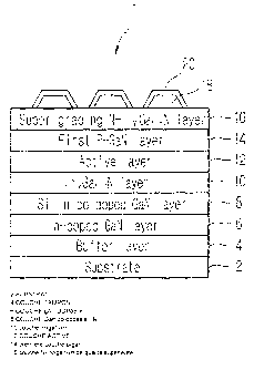
FIG. 1 schematically illustrates a layered structure of a nitride
semiconductor light emitting diode according to the first embodiment of the
present invention;
FIG. 2 schematically illustrates a layered structure of a nitride
semiconductor light emitting diode according to the second embodiment of the
present invention; and
FIG. 3 schematically illustrates a layerecl structure of a nitride
semiconductor light emitting diode according to the third embodirnent of the
present invention.
[Mode for Invention]
Hereinafter, preferred embodiments of the present invention will be
c[escribed in detail with reference to accompanying drawings.
FIG. .1 schematically illustrates a layered structure of a nitride
3
CA 02599881 2007-04-27
WO 2007/102627 PCT/KR2005/002173
semiconductor light emitting diode according to the first embodiment of the
present invention.
In the inventive nitride semiconductor light emitting diode 1, a buffer
layer 4 is formed on a substrate 2 as shown in FIG. 1. The buffer layer 4 can
be formed to have any one of an AlInN/GaN layerecl structure, an InxGal-XN/GaN
layered structure, and an AlXIn,,Ga1-(X+yN/InYGal-xN/GaN layered structure,
An In-doped GaN layer 6 is formed on the buffer layer 4, and an N-type
first electrode layer is formed on the In-doped GaN layer 6. The N-type first
electrode layer can employ a Si-In co-doped GaN layer 8 having silicon (Si)
and
incliLim (In) concurrently doped therein.
Further, a low-mole first InJZGal-aN layer 10 having a low content of
indium is formed on the Si-In co-doped GaN layer 8, and an active layer 12
emitting light is formed on the first InxGal-,;N layer 10. The active layer 12
can
be provided in a single quantum well structure or a multi quantum well
structure
having InGaN well layer/InGaN barrier layer. Its layered structure will be
later
described with reference to FIG. 3 in more detail.
After that, the first P-GaN layer 14 is formed on the active layer 12.
The first P-GaN layer 14 can have magnesium doped therein.
An N-type second electrode layer is formed on the first P-GaN layer 14.
The N-type second electrode layer can employ a super grading N-InxGal-XN
layer 16 whose energy band gap is controlled by sequentially varying an indium
composition. The super grading N-In,;Gal-aN layer 16 can be formed to have a
composition range (x) of 0 to 0.2.
Considering that the first electrode layer 8 and the second electrode
layer 16 are all formed of N-type nitride, and have the first P-GaN layer 14
interposed therebetween, the inventive nitride semiconductor light emitting
cliocle can be analyzed to have a structure of an NPN junction light emittirig
diode
unlike a related art PN junction light emitting diode.
A second P-GaN layer 18 is partially formed on the super grading
N-In,,Gai-,;N layer 16 to have a protrusive convex shape, and an N-InXGal-.,N
layer 20 being a third electrode layer is formed on the second P-GaN layer 18.
The second P-GaN layer 18 and the third electrode layer 20 have the same or
similar structure with the first P-GaN layer 14 and the second electrode
layer,
ancl can be formed through the following fabrication process.
In other words, first, an insulating film is partially formed on the super
gracling N-InxGal-~N layer 16 to partially expose the super grading N-InXGaI-
XN
layer 16. After that, the second P-GaN layer 18 and the N-In,;Gal-XN layer 20
are formed on the exposed super grading N-InxGal-,N layer 16. Next, the
insulating film is removed.
At this time, mas'king is selectively performed using the insulating film in
various types, and the N/P nitride semiconductors 20 and 18 can be again
grown-up on the second electrode layer 16 to have various types of size, shape
4
CA 02599881 2007-04-27
WO 2007/102627 PCT/KR2005/002173
and depth. According to the present invention, an external quantum efficiency
can be improved by selectively removing a portion masked with the insulating
film and forming an indented portion (convex portion) on a surface of the
light
emitting diode.
In the related art PN junction light emitting diocle, its surface was
partially etched and indent-shaped (convex-shaped). Such an etching
technique has a disadvantage in that a damage of a P-GaN surface is caused,
and accordingly a contact resistance is increased, thereby reducing a current
injection effect and reducing a light output. Further, it has a disadvantage
in
that when a high current is applied, a high contact resistance causes the
generation of heat, thereby causing a serious influence on a-reliability of
device.
Further, the N-type nitride semiconductors (for example, the super
grading N-InXGaI-,,N layers 16 and 20) used as the second and third electrode
layers have a lower resistance than a related art P-GaN contact layer and
accordingly, its contact resistance can be reduced, thereby maximizing the
injection of current. Further, the second and third electrode layers can
employ
all of a light transmission electrode and a light non-transmission electrode
as
electrodes for applying a bias voltage. The light transmission electrode can
employ a transmission resistant metal layer or a transmission metal-oxide
layer
with the maximization of current spreading and an excellent light transmission
so as to maximize the light output. Such material can employ Indium-Tin-Oxide
(ITO), Zinc Oxide (ZnO), rhthenium oxide (RuOx), iridium oxide (IrOx), and
nickel
oxicle (Ni0) or an aurum (Au) alloy metal containing nickel (Ni). The
electrode
can be formed on the second electrode layer 16 and the third electrode layer
20.
FIG. 2 schematically illustrates a layered structure of a nitride
semiconductor light emitting diode according to the second embocliinent of the
present inveiltion.
In the inventive layered structure of the nitride semiconductor light
emitting diode 21, only second and third electrode layers are different from
those of the nitride semiconductor light emitting diode 1. Accordingly, only
the
second and third electro,de layers will be described below..
In other words, in the inventive nitride semiconductor light emitting diode
21, first and second InGaN/AIInGaN super lattice structure layers 26 and 30
are
formed as the second and third electrode layers. The first and second
InGaN/AIInGaN super lattice structure layers 26 and 30 can also have silicon
clopecl therein.
By forming the above layered structure, an N/P/N light emitting diode can
be realized. The N/P/N light emitting diode is selectively masked on its
surface,
using an insulating film, only a N/P nitride s'emiconductor is again grown up,
and
then the selectively masking insulating film is removed, thereby completing
the
light emitting diocle having a convex (inclented) shape.
Though not illustrated in the drawings, first and second InGaN/InGaN
CA 02599881 2007-04-27
WO 2007/102627 PCT/KR2005/002173
super lattice structures can be also formed as the second and third electrode
layers, and also can have silicon doped therein.
Thus, a structure of an active layer adopted in a nitride semiconductor
light emitting cliocle 31 according to the present invention will be in more
detail
clescribed with reference to FIG. 3. FIG. 3 schematically illustrates a
layered
structure of the nitride semiconductor light emitting diode according to the
third
embodiment of the present invention. In the layered structure of FIG. 3, a
clescription of the layer (denoted by the same reference numeral) of FIG. 1
will
be omittecl.
As shown in FIG. 3, the inventive nitride semiconductor light emitting
diode 31 has a low-mole InXGal-XN layer 10 having a low content of indium for
controlling a strain of the active layer, so as to increase an internal
quantum
efficiency. Further, the inventive nitride semiconductor light emitting diode
31
further includes a first SiNa cluster layer 33 and a second SiNx cluster layer
35,
which are controlled in an atomic scale, below and on the low-mole InXGal_xN
layer 10 so as to improve a reverse leakage current and the light output
resulting from the fluctuation of indium.
Further, the active layer emitting the light can be formed to have a single
quantum well structure or a multi quantum well structure constituted of
In,.Gal-,,N well layer/InzGal-ZN barrier layer.
FIG. 3 shows an example of the light emitting diode having the multi
quantum well structure further including SiNX cluster layers 39 and 45, which
are respectively interposed between InYGal-,,N well layers 37 and 43 and
InZGaI-ZN barrier layers 41 and 47. Here, the In,,Gal-,,N well layer/SiNx
cluster
layer/InZGaI-zN barrier layer can be also controlled to have a composition
ratio
of 0<y<0.35 and 0<z<0.1, in order to improve an efficiency of light emission
of
the active layer. Considering a relation with the low-mole InaGal-,;N layer 10
having the low content of indium, the content of indium doped into the
In1,Gal_YN
well layers 37 and 43/InZGal-ZN barrier layers 41 and 47, and the content of
indium doped into the low-mole In,Gal,N layer 10 can be controlled to have
values of 0<x<0.1, 0<y<0.35,:and 0<z<0.1.
Though not illustrated in the drawings, but a GaN cap layer for controlling
an amount of incliuin fluctuation of the In,,Gal-,,N well layer can be also
formed
between the In,,Gal-,,N well layer and the InZGal-ZN barrier layer
constituting the
active layer. Here, the well layer and the barrier layer emitting the light
can
respectively have the indium contents to provide a configuration of
In,.Gal-yN(0<y<0.35)/GaN cap/InZGaI-ZN(0<z<0.1).
After the last layer of the active layer having the single quantum well
layer or the multi quantum well structure is -grown-up, and then the SiNx
layer
49 is again grown-up at a thickness of atomic scale, thereby suppressing a
diffusion of magnesium (Mg) of the first P-GaN layer 14 into the active layer.
FIG. 3 illustrate a case where the second electrode layer employs the
6
CA 02599881 2007-04-27
WO 2007/102627 PCT/KR2005/002173
super grading N-InGal-XN layer 16, but the second electrode layer can also
employ the InGaN/AIInGaN super lattice structure layer or the InGaN/InGaN
super lattice structure layer.
Though not illustrated in the above embodiments (FIGS. 1 to 3), but an
electrode (or an electrode pad) of the first electrode layer is formecl on the
first
electrode layer after a partial etching up to the first electrode layer of the
nitride semiconductor, and an electrode pad can be additionally formed on the
transparent electrode formed on the second or third electrode layer.
As described above, in the inventive nitride semiconductor light emitting
diode, the N/P/N junction light emitting diode structure can be applied to
reduce
an operation voltage while to improve current injection, thereby improving a
phenomenon of current concentration resulting from the high contact resistance
of the P-GaN layer itself used as the P-type electrocle layer in the related
art
P/N junction light emitting diode. Further, only the N/P junction layer is
selectively again grown up using the insulating film, and the indention
portion
(convex portion) is foi-ined on the surface of the light emitting diocle,
thereby
increasing the external quantum efficiency.
The inventive nitride semiconductor light emitting diode is an
(N/P)/NIP/N junction light emitting diode for reducing a surface damage
occurring~ in the partial etching of the related art P-GaN surface and its
operation voltage, increasing the external quantum efficiency of the light
einitting diode, providing an excellent crystallinity through re-growth, and
fundamentally improving the internal quantum efficiency.
Further, the inventive nitride semiconductor light emitting diode has a
structure having the first electrode layer and the second electrode layer
formed
of an N-type nitride serniconductor, and specifically improving the contact
resistance of the second electrode layer, thereby improving the light output.
[Industrial Applicability]
In a nitride semiconductor light emitting device and a fabrication method
thereof according to the present invention, the active layer constituting the
nitride semiconductor light emitting diode is improved in crystallinity, light
output, and reliability.
7