Note : Les descriptions sont présentées dans la langue officielle dans laquelle elles ont été soumises.
CA 02600858 2007-08-10
WO 2007/081360 PCT/US2006/006316
ELECTRONIC DISABLING DEVICE HAVING ADJUSTABLE
OUTPUT PULSE POWER
FIELD OF THE INVENTION
The present invention relates generally to the field of an electronic
disabling device
for immobilizing a live target. More specifically, the present invention is
related to an
electronic disabling device having adjustable output pulse power and a method
for providing
the same.
BACKGROUND OF THE INVENTION
An electronic disabling device can be used to refer to an electrical discharge
weapon
or a stun gun. The electrical discharge weapon connects a shocking power to a
live target by
the use of darts projected with trailing wires from the electrical discharge
weapon. The
shocks debilitate violent suspects, so peace officers can more easily subdue
and capture them.
The stun gun, by contrast, connects the shocking power to the live target that
is brought into
direct contact with the stun gun to subdue the target. Electronic disabling
devices are far less
lethal than other more conventional weapons such as firearms.
In general, the basic ideas of the above described electronic disabling
devices are to
disrupt the electric communication system of muscle cells in a live target.
That is, an
electronic disabling device generates a high-voltage, low-amperage electrical
charge. When
the charge passes into the live target's body, it is combined with the
electrical signals from the
brain of the live target. The brain's original signals are mixed in with
random noise, making
it very difficult for the muscle cells to decipher the original signals. As
such, the live target is
stunned or temporarily paralyzed. The current of the charge may be generated
with a pulse
frequency that mimics a live target's own electrical signal to further stun or
paralyze the live
target.
To dump this high-voltage, low-amperage electrical charge, the electronic
disabling
device includes a shock circuit having multiple transformers and/or
autoformers that boost
the voltage in the circuit and/or reduce the amperage. The shock circuit may
also include an
oscillator to produce a specific pulse pattern of electricity and/or
frequency.
Current electronic disabling devices take the lower voltage, higher current of
a battery
or batteries and convert it into a higher voltage, lower current output. This
output must
contact an individual in two places to create a full path for the energy to
flow. For stun guns,
this output is provided to two metal contacts on the contacting side of the
device that are a
short distance apart. On the electronic discharge weapons, this output is
provided to two
metal darts (or probes) that are propelled into the live target (or
individual). The distance
between the probes is normally larger than the stun gun contacts to allow for
a greater effect
of the live target. The metal probes are connected to the electrical circuitry
in the device by
thin conducting wires that carry the energy from/to the device and from/to the
metal probes.
-1-
CA 02600858 2007-08-10
WO 2007/081360 PCT/US2006/006316
With the current devices, only one level of output power is available per
device package.
Therefore a larger than necessary high voltage waveform may be used on a
target that could
have been sufficiently immobilized by a lower high voltage waveform.
In view of the foregoing, it would be desirable to create an electronic
disabling device
for immobilization and capture of a live target having a power control having
selectable
power levels such that the electronic disabling device does not apply a power
level to a live
target that might possibly be unsafe to that particular individual.
SUMMARY OF THE INVENTION
The present invention relates to a system andlor an associated method for
providing
an electronic disabling device with a level of power control. The invention
provides the
electronic disabling device with multiple selectable power levels in one
device package. This
would allow a user of the electronic disabling device to start with a low
power setting (e.g.,
the lowest power setting) and if the power was not effective, incrementally
increase the
power until it was effective. This adds a level of safety such that the user
does not apply a
power level to a live target that might possibly be unsafe to that particular
individual.
In one exeinplary embodiment of the present invention, an electronic disabling
device
has multiple adjustable power levels to immobilize a live target. The
electronic disabling
device includes a battery, an initial ste -u volta e circuit, a final ste -u
transformer e.
p p g P P ( g=, a
plain transformer, an autoformer, etc.), a first electrical output contact, a
second electrical
output contact, and a power control circuit. The initial step-up voltage
circuit is coupled to
receive an initial power from the battery. The final step-up transformer
provides an output
power. The output power is received by the first electrical output contact,
and the second
electrical output contact receives the output power from the first electrical
output through the
live target. Here, the power control circuit is coupled between the initial
step-up voltage
circuit and the final step-up transformer to adjust the power levels of the
output power
provided by the final step-up transformer.
In one exemplary embodiment of the present invention, a method provides an
electronic disabling device with multiple adjustable power levels to
immobilize a live target.
The method includes: providing an input power from a battery to an initial
step-up voltage
circuit; stepping-up a voltage of the input power through the initial step-up
voltage circuit;
adjusting and transforming the input power to an output power having an
adjusted power
level through a final step-up transformer(e.g., a plain transformer, an
autoformer, etc.); and
providing the output power having the adjusted power level to an electrical
output contact.
Here, the adjusted power level of the output power is selected by a user of
the electronic
disabling device.
A more complete understanding of the electronic disabling device having
adjustable
output pulse power will be afforded to those skilled in the art and by a
consideration of the
-2-
CA 02600858 2007-08-10
WO 2007/081360 PCT/US2006/006316
following detailed description. Reference will be made to the appended sheets
of drawings
which will first be described briefly.
BRIEF DESCRIPTION OF THE DRAWINGS
The accompanying drawings, together with the specification, illustrate
exemplary
embodiments of the present invention, and, together with the description,
serve to explain the
principles of the present invention.
FIG. 1 illustrates an exemplary electronic disabling device.
FIG. 2 illustrates an exemplary electronic disabling device using a relaxation
oscillator.
FIG. 3 illustrates an exemplary electronic disabling device using an
independently
driven oscillator.
FIG. 4 illustrates an exemplary electronic disabling device having a load
parallel to a
primary coil.
FIG. 5 illustrates an exemplary electronic disabling device having multiple
taps.
FIG. 6 illustrates an exemplary electronic disabling device for producing a
sinusoidal
output waveform.
FIG. 7 illustrates an exemplary electronic disabling device for producing a
half-cycle
uni-pulse output waveform.
FIG. 8 illustrates an exemplary sinusoidal output waveform.
FIG. 9 illustrates an exemplary half-cycle uni-pulse output waveform.
FIG. 10 illustrates an exemplary electronic disabling device for producing a
sinusoidal
output waveform having multiple spark gaps.
FIG. 11 illustrates an exemplary electronic disabling device for producing a
half-cycle
uni-pulse output waveform having multiple sparlc gaps.
DETAILED DESCRIPTION
In the following detailed description, only certain exemplary embodiments of
the
present invention are shown and described, by way of illustration. As those
skilled in the art
would recognize, the described exemplary embodiments may be modified in
various ways, all
without departing from the spirit or scope of the present invention.
Accordingly, the
drawings and description are to be regarded as illustrative in nature, and not
restrictive.
There may be parts shown in the drawings, or parts not shown in the drawings,
that
are not discussed in the specification as they are not essential to a complete
understanding of
the invention. Like reference numerals designate like elements.
Referring to FIG. 1, an example of an electronic disabling device is shown to
include
a battery 10, an initial step-up voltage circuit 20, a trigger (not shown), a
final step-up
transformer 30, a first electrically conductive output contact (or probe) 50,
and a second
-3-
CA 02600858 2007-08-10
WO 2007/081360 PCT/US2006/006316
electrically conductive output contact (or probe) 60. Each of the contacts 50,
60 can be
connected to the housing of the electronic disabling device by electrically
conductive wires.
Further, although the final step-up transformer 30 is exemplary shown in FIG.
1 as being a
plain transformer, it should be recognized by those skilled in the art that
the present invention
is not thereby limited. For example, a final step-up transformer according to
an embodiment
of the present invention can be realized as being an autoformer.
In operation, an electrical charge which travels into the contact 50 is
activated by
squeezing the trigger. The power for the electrical charge is provided by the
battery 10. That
is, when the trigger is turned on, it allows the power to travel to the
initial step-up voltage
circuit 20. The initial step-up voltage circuit 20 includes a first
transformer that receives
electricity from the battery 10 and causes a predetermined amount of voltage
to be
transmitted to and stored in a storage capacitor through a number of pulses.
Once the storage
capacitor stores the predetermined amount of voltage, it is able to discharge
an electrical
pulse into the final step-up transformer 30 (e.g., a second transformer and/or
autoformer).
The output from the final step-up transformer 30 then goes into the first
contact 50. When
the first and second contacts 50, 60 contact a live target, charges from the
first contact 50
travel into tissue in the target's body, then through the tissue into the
second contact 60, and
then to a ground. Pulses are delivered from the first contact 50 into target's
tissue for a
predetermined number of seconds. The pulses cause contraction of skeletal
muscles and
malce the muscles inoperable, thereby preventing use of the muscles in
locomotion of the
target.
In one embodiment, the shock pulses from an electronic disabling device can be
generated by an oscillator such as a classic relaxation oscillator that
produces distorted saw-
tooth pulses to the storage capacitor. An electronic disabling device having
the relaxation
oscillator is shown as FIG. 2.
Referring to FIG. 2, power is supplied to the relaxation oscillator from a
battery
source 160. The closure of a switch SWl connects the battery source 160 with
an inverter
transformer TI. In FIG. 2, a tickler coil 110 of the inverter transformer T1
between PAD1
and PAD2 is used to form the classic relaxation oscillator. A primary coil 100
of the inverter
transfoimer Tl is connected between PAD3 and PAD4. Upon closure of the power
switch
SW1, the primary coil 100 of the inverter transformer T1 is energized as a
current flows
through the coil 100 from PAD3 to PAD4 as the power transistor Q1 is turned
ON. The
tickler coil 110 of the inverter transformer Tl is energized upon closure of
the power switch
SW1 through a resistor R8 and a diode D3. The current through the ticlder coil
110 also
forms the base current of the power transistor Q1, thus causing it to turn ON.
Since the
ticlder coil 110 and the primary coil 100 of the inverter transformer T1
oppose one another,
the current through power transistor Ql causes a flux in the inverter
transformer T1 to, in
effect, baclcdrive the tickler coil 110 and cut off the power transistor Q1
base current, thus
causing it to turn OFF and forming the relaxation oscillator.
-4-
CA 02600858 2007-08-10
WO 2007/081360 PCT/US2006/006316
In addition, a secondary coil 120 of the inverter transformer TI between PAD5
and
PAD6 is connected to a pair of diodes D4 and D5 that form a half-wave
rectifier. The pair of
diodes D4 and D5 are then serially connected with a sparlc gap 130 and then
with a primary
coil 140 of the output transformer T2. The primary coil 140 of the output
transformer T2 is
connected between PAD7 and PAD8. The sparlc gap 130 is selected to have
particular
ionization characteristics tailored to a specific sparlc gap breakover voltage
to "tune" the
output of the shock circuit.
In more detail, when sufficient energy is charged on a storage capacitor, a
gas gap
breaks down on the spark gap 130 such that the spark gap 130 begins to conduct
electricity.
This energy is then passed through the primary coil 140 of output or step up
transformer T2.
However, the present invention is not limited to the above described exemplary
embodiment. For example, an embodiment of an electronic disabling device can
include a
digital oscillator coupled to digitally generate switching signals or an
independent oscillator
210 as shown in FIG. 3.
In the disabling device of FIG. 3, a power is supplied from a battery source
230 to an
inverter transformer TI'. In FIG. 3, a primary coil 240 of the inverter
transformer T1' is
connected between PAD10 and PAD11. A power switch 250 is connected between the
inverter transformer T1' and a ground. The power switch 250 (or a base or a
gate of the
power switch 250) is also connected to the independent oscillator 210.
In more detail, the primary coil 240 of the inverter transformer T1' is
energized as
current flows through the coi1240 from PAD 10 to PAD 11 as the switch (or
transistor) 250 is
turned ON. The independent oscillator 210 is coupled to the switch 250 (e.g.,
at the base or
the gate of the switch 250) to turn the switch 250 ON and OFF. A secondary
coil 260 of the
inverter transformer Tl' between PAD 12 and PAD 13 is connected to a full-wave
rectifier 270.
The full-wave rectifier 270 is then serially connected with a spark gap 280
and then with a
primary coil 290 of the output transformer T2'. The primary coil 290 of the
output
transformer T2' is connected between PAD 14 and PAD 15.
In operation, the oscillator 210 creates a periodic output that varies from a
positive
voltage (V+) to a ground voltage. This periodic waveform creates the drive
function that
causes current to flow through the primary coil 240 of the transformer Tl'.
This current flow
causes current to flow in the secondary coil 260 of the transformer Tl' based
on the turn ratio
of the transformer T1'. A power current from the battery source 230 then flows
in the
primary coil 240 of the transforrner T1' only when the switch 250 is turned on
and is in the
process of conducting. The full wave bridge rectifier 270 then rectifies the
voltage from the
power source 230 when the switch 250 is caused to conduct.
In view of the foregoing, electronic disabling devices with high powered
shocks can
be formed. However, the propriety of forming weapons capable of producing such
high
powered shocks may be in question because the enhanced shocks may increase the
weapons
lethality, especially where circuits operating at a fraction of the power
ranges that can be
-5-
CA 02600858 2007-08-10
WO 2007/081360 PCT/US2006/006316
achieved by these disabling devices (e.g., at power levels as low as 1.5 watts
and 0.15 joules
per pulse at ten pps) can completely disable most test subjects. In addition,
some seventy
deaths have occurred proximate to use of such weapons. As such, using these
weapons at
high power may run contrary to the idea that electronic disabling devices are
intended to
subdue and capture live targets without seriously injuring them.
In accordance with an embodiment of the present invention, an electronic
disabling
device is provided with multiple selectable power levels in one device
package. This would
allow a user of the electronic disabling device to start with a low power
setting (e.g., the
lowest power setting) and if the power was not effective, incrementally
increase the power
until it was effective. This adds a level of safety such that the user does
not apply a power
level to a live target that might possibly be unsafe to that particular
individual.
Referring to FIG. 4, an electronic disabling device in accordance with one
embodiment of the present invention includes a battery 310, an initial step-up
voltage circuit
320, a trigger (not shown), a final step-up transformer 330, a first
electrically conductive
output contact (or probe) 350, and a second electrically conductive output
contact (or probe)
360. Also, in FIG. 4, a primary coil (or winding) 370 of the final step-up
transformer 330 is
connected between a first node 380a and a second node 380b. In this
embodiment, an
electrical switching device 385 and a load 387 are also shown to be connected
between the
first node 380a and the second node 380b and in parallel with the coil 370.
The load 387 can
be a resistive, capacitive, and/or inductive load. The switching device 385 is
connected with
and controlled by a control logic 390. As such, the electrical switching
device 385 of FIG. 4
allows switching in (and out) the parallel load 387 to the primary coil 370 of
the final step-up
transformer 330.
In more detail, the switching device 385 would be controlled by the additional
control
logic 390 added to the circuit 320 of the electronic disabling device. The
additional control
logic 390 allows a control input from a user such that the output pulse power
of the electronic
disabling device can be adjusted by either switching in or switching out the
parallel load 387
to the primary coil 370 of the final step-up transformer 330.
Referring to FIG. 5, an electronic disabling device in accordance with another
embodiment of the present invention includes a battery 410, an initial step-up
voltage circuit
420, a trigger (not shown), a final step-up transformer 430, a first
electrically conductive
output contact (or probe) 450, and a second electrically conductive output
contact (or probe)
460. Also, in FIG. 5, a primary coil (or winding) 470 of the final step-up
transformer 430
includes a first tap 470a, a second tap 470b, and a third tap 470c. In this
embodiment, a first
electrical switching device 485a is shown to be connected between the first
tap 470a and a
first node 480a, a second electrical switching device 485b is shown to be
connected between
the second tap 370b and a second node 480b, and a third electrical switching
device 485c is
shown to be connected between the third tap 470c and a third node 480c. The
first, second,
and third switching devices 485a, 485b, and 485c are connected with and
controlled by a
-6-
CA 02600858 2007-08-10
WO 2007/081360 PCT/US2006/006316
control logic 490. As such, the electrical switching devices 485a, 485b, and
485c of FIG. 5
change the primary coil 470 of the final step-up transformer 430 from a single
winding
configuration (e.g., as shown in FIG. 1) to a multiple winding configuration
with the first,
second, and third taps 470a, 470b, and 470c.
In more detail, the electrical switching devices 485a, 485b, and 485c allow
the
primary coil 470 to be shortened using the first, second, and third taps 470a,
470b, and 470c
of the primary coil 470 and connecting them to the first, second, and third
nodes (or a
ground) 480a, 480b, and 480c, respectively. This can effectively reduce the
number of
windings in the primary coil 470 such that a smaller step-up voltage can be
obtained on a
secondary coil 475 connected witlz the first and second electrically
conductive output contacts
450 and 460. Any number of taps can be added to the primary winding, and the
present
invention is not thereby limited by the embodiment of FIG. 5. Also, the
control logic 490 is
added to control the switching devices 485a, 485b, and 485c to allow a control
input from a
user. In addition, this control logic 490 is connected to the initial step-up
voltage circuit 420
via a connection 425 to allow for an adjustment of the pulse rate of the
initial step-up voltage
circuit 420 to keep the same output pulse rate for the device.
FIG. 6 shows a view into an initial step-up circuit of an electronic disabling
device
connected with a final step-up transformer of the electronic disabling device.
The initial step-
up circuit includes a power supply 585 having an oscillator (e.g., the
oscillator shown in
FIGs. 2 or 3 for providing a pulse rate), a bridge rectifier 580, a spark gap
SG1, and a storage
capacitor Cl. Here, the storage capacitor Cl is connected to a primary coil
570 of the final
step-up transfoimer in series, and the spark gap SGI is connected to the
storage capacitor Cl
and the primary coil 570 in parallel. As such, the spark gap SG1 and the
storage capacitor Cl
are positioned to provide a sinusoidal output waveform as shown in FIG. 8.
In more detail, an energy from the bridge rectifier 580 of the initial step-up
voltage
circuit (e.g., a full-wave bridge rectifier circuit having at least four
diodes) is initially used to
charge up one plate of the storage capacitor Cl. The spark gap SG1 fires
whenever the
voltage of the storage capacitor Cl reaches a fixed brealcdown voltage of the
spark gap SGI,
and the stored energy discharges through the primary coil 570. In addition,
because the
storage capacitor Cl and the primary coil 570 are connected to create a tank
circuit, as the
capacitor Cl discharges, the primary coil 570 will try to keep the current in
the circuit
moving, so it will charge up the other plate of the capacitor C1. Once the
field of the primary
coil 570 collapses, the capacitor Cl has been partially recharged (but with
the opposite
polarity), so it discharges again through the primary coil 570. As such, the
sinusoidal output
waveform as shown in FIG. 8 is provided by the electronic disabling device of
FIG. 6.
Alternatively, as shown in FIG. 7, a spark gap SGl' is connected to a primary
coil
570' of a final step-up transformer in series, and a storage capacitor Cl' is
connected to the
spark gap SG1' and the primary coil 570' in parallel. As such, the spark gap
SG1' and the
storage capacitor Cl' are positioned to provide a half-cycle uni-pulse output
waveform as
-7-
CA 02600858 2007-08-10
WO 2007/081360 PCT/US2006/006316
shown in FIG. 9.
In more detail, the spark gap SG1' and the storage capacitor Cl' of FIG. 7 are
positionally switched as compared to the spark gap SGI and the storage
capacitor Cl to
remove the tank circuit and to produce the half-cycle uni-pulse output
waveform as shown in
FIG. 9. As such, the electronic disabling device of FIG. 7 produces a mostly
positive half-
cycle pulse waveform or a mostly negative half-cycle pulse waveform. Also,
this indicates
that electrons flow mainly in one direction with fewer electrons flowing in
the opposite
direction. That is, the opposite amplitude in the sinusoidal output waveform
of FIG. 8 is
caused by the electrons flowing in the opposite direction for part of the
cycle.
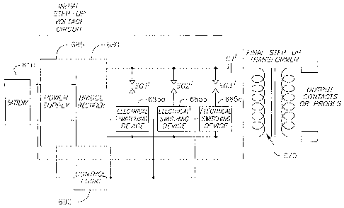
Referring to FIG. 10, an electronic disabling device in accordance with one
embodiment of the present invention includes a battery 610, a power supply
685, a bridge
rectifier circuit 680 of an initial step-up voltage circuit, a trigger (not
shown), and a primary
coil 670 of a final step-up transformer. In addition, the electronic disabling
device of FIG. 10
includes a first spark gap SGl', a second spark gap SG2', a third spark gap
SG3', and a
storage capacitor Cl'. Here, the storage capacitor C1' is connected to the
primary coil 670 of
the final step-up transformer in series. Also, as shown in FIG. 10, a first
electrical switching
device 685a is used to connect/disconnect the first spark gap SG1' to the
storage capacitor Cl'
and the primary coil 670 in parallel, a second electrical switching device
685b is used to
connect/disconnect the second sparlc gap SG2' to the storage capacitor C1' and
the primary
coil 670 in parallel, and a third electrical switching device 685c is used to
connect/disconnect
the third spark gap SG3' to the storage capacitor C1' and the primary coil 670
in parallel. The
first, second, and third switching devices 685a, 685b, and 685c are connected
with and
controlled by a control logic 690. As such, the multiple spark gaps SG1',
SG2', and SG3' and
switching devices 685a, 685b, and 685c allow a user of the electronic
disabling device to
adjust the output power of the device. That is, by allowing the user of the
electronic
disabling device to select the appropriate spark gaps SGI', SG2', and SG3',
the output power
of the electronic disabling device of FIG. 10 can be controlled. Here, the
control logic 690
for the selectable sparlc gaps SGI', SG2', and SG3' would also provide an
input to the power
supply 685 including an oscillator to keep the same output pulse rate.
Referring to FIG. 11, an electronic disabling device in accordance with
another
embodiment of the present invention includes a battery 710, a power supply
785, a rectifier
circuit 780 of an initial step-up voltage circuit, a trigger (not shown), and
a primary coil 770
of a final step-up transformer. In addition, the electronic disabling device
of FIG. 11 includes
a first sparlc gap SG1", a second spark gap SG2", a third sparlc gap SG3", and
a storage
capacitor C1". Here, a first electrical switching device 785a is used to
connect/disconnect the
first sparlc gap SG1' to the primary coil 770 in series, a second electrical
switching device
785b is used to connect/disconnect the second spark gap SG2" to the primary
coil 770 in
series, and a third electrical switching device 785c is used to
connect/disconnect the third
sparlc gap SG3" to the primary coil 770 in series. In addition, as shown in
FIG. 11, the
-8-
CA 02600858 2007-08-10
WO 2007/081360 PCT/US2006/006316
storage capacitor C1" is connected to the primary coil 770 of the final step-
up transformer in
parallel with at least one of the spark gaps SG1", SG2", and SG3" connected to
the primary
coil 770 in series. The first, second, and third switching devices 785a, 785b,
and 785c are
connected with and controlled by a control logic 790. As such, the multiple
spark gaps SG1",
SG2", and SG3" and switching devices 785a, 785b, and 785c allow a user of the
electronic
disabling device to adjust the output power. That is, similar to the device of
FIG. 10, by
allowing the user of the electronic disabling device to select the appropriate
spark gaps SG1",
SG2", and SG3", the output power of the electronic disabling device of FIG. 11
can be
controlled. Here, the control logic 790 for the selectable spark gaps SG1",
SG2", and SG3"
would also provide input to the power supply 785 including an oscillator to
keep the same
output pulse rate.
In view of the forgoing, FIGs. 10 and 11 show that, by adding multiple spark
gaps and
switching devices, the output power of an electronic device can be adjusted in
a way that
differs from the embodiments of FIGs. 4 and 5 for either the sinusoidal output
waveform or
the half-cycle uni-pulse output waveform. In FIGs. 10 and 11, the spark gaps
control how
much voltage is stored on the storage capacitor by not making a complete
circuit until a
particular voltage is reached. That is, the spark gaps according to an
embodiment of the
present invention include at least a first spark gap having a first breakdown
voltage and at
least a second spark gap having a second breakdown voltage diffeiing from the
first break
down voltage. The controlled spark gaps (e.g., SGl', SG2', SG3' or SGl", SG2",
SG3") then
only provide a complete circuit for a very small amount of time for allowing
the storage
capacitor (e.g., C1' or C1 ") to dump energy into the primary coil (e.g., 670
or 770) of the final
step-up transformer.
While the invention has been described in connection with certain exemplary
embodinients, it is to be understood by those skilled in the art that the
invention is not limited
to the disclosed embodiments, but, on the contrary, is intended to cover
various modifications
included within the spirit and scope of the appended claims and equivalents
thereof.
35
-9-