Note : Les descriptions sont présentées dans la langue officielle dans laquelle elles ont été soumises.
CA 02601530 2007-09-07
Aperture-coupled antenna
Description
The present invention generally relates to an aperture-
coupled antenna, particularly to an aperture-coupled
circularly polarized planar antenna.
Wireless systems which have to function in several
frequency bands are being developed more frequently.
Frequently, compact antennas are necessary to keep the
setup volume of the antennas small and to allow usage in
portable devices.
It is possible to provide a separate antenna for each
frequency band to be used. The disadvantage of using
separate antennas, however, is that a multiplexer has to be
employed. In addition, the area necessary for the antennas
increases when using separate antennas.
Receiving from several different wireless transfer systems
by a single broadband antenna is problematic since
broadband antennas cannot usually be manufactured at low
cost in a compact design. If all the relevant systems are
to be received by a single broadband antenna, this will not
be possible using a small cheap antenna.
A multi-element antenna having a special radiator for every
frequency range can be used for receiving several frequency
bands. Most antenna concepts known which are suitable for
receiving from two or more frequency bands (dual-band
concept and/or multiband concept) and which can be used for
and/or in patch antennas, such as, for example, integrated
inverted-F antennas (IFAs) and planar inverted-F antennas
(PIFAs) , comprise only a linear polarization. Well-known
antenna shapes of this kind are, for example, described in
the book "Planar Antennas for Wireless Communications" by
CA 02601530 2007-09-07
- 2 -
Kin-Lu Wong (John Wiley & Sons, Inc., Hoboken, New Jersey,
2003).
However, it is desirable in particular for mobile
applications to use a circular polarization, since in this
case the orientation of transmitting and receiving antennas
is uncritical, whereas when using linear polarization, the
orientation of the antennas has to be selected
appropriately.
A series of antennas which may be integrated comprising a
circular polarization are known, however many of the
geometries which may be integrated comprise essential
disadvantages for generating a circular polarization.
Exemplarily, nearly squared patches (planar conductive
areas) of coaxial feeding have a low impedance bandwidth,
as is, for example, described in the dissertation
"Untersuchung und Aufbau von Multibandigen Antennen zum
Empfang zirkular polarisierter Signale" by U. Wiesman
produced in 2002 at the Fraunhofer-Institut fur integrierte
Schaltuiigen in Erlangen. The same is true for aperture-
coupled patch antennas having a cross-slot which are
described in the master paper having the title
"Untersuchung zirkular polarisierter Patchantenne mit
Aperturkopplung" by A. Popugaev in 2004 for Fraunhofer
Institut fiar integrierte Schaltungen in Erlangen. All in
all, it can be stated that the polarization purity in known
broadband circularly polarized patch antennas having only
one feeding point is low. On the other hand, spiral
antennas exhibit great losses.
An overview of aperture-coupled microstrip antennas can be
found in the article "A review of aperture coupled
microstrip antennas: history, operation, development and
applications" by D.M. Pozar, published in May 1996 at the
University of Massachusetts at Amherst and is available on
the internet under
www.ecs.umass.edu/ece/pozar/aperture.pdf. Further
CA 02601530 2007-09-07
- 3 -
information on the topic of broadband patch antennas can be
found in the book "Broadband Patch Antennas" by J.-F.
Zuercher published in 1995 by the Artech-House Verlag.
In summary, it can be stated that in the prior art there is
no technologically advantageous antenna design which, with
good radiation efficiency and sufficient impedance
bandwidth, allows circularly polarized waves to be radiated
with high orthogonal polarization suppression. In addition,
there is no known technologically simple antenna design
which can be realized at low cost which, with good
efficiency and sufficient bandwidth, allows a circularly
polarized electromagnetic wave to be radiated in two
different frequency bands.
It is the object of the present invention to provide an
aperture-coupled patch antenna which allows radiation of a
circularly polarized electromagnetic wave and which
comprises both a good orthogonal polarization suppression
and a great impedance bandwidth compared to conventional
antennas.
This object is achieved by an antenna according to claim 1.
The present invention provides an aperture-coupled antenna
comprising a first radiation electrode, a ground area and a
wave gu-i_de implemented to supply energy to the antenna. The
wave guide is arranged spaced apart from the ground area on
a first side of the ground area, and the radiation
electrode is arranged spaced apart from the ground area on
a second side of the ground area. The ground area comprises
an aperture including a first slot in the ground area, a
second slot in the ground area and a third slot in the
ground area, wherein the first slot and the second slot
together form a slot in the shape of a cross, and wherein
the third slot passes an intersection of the first slot and
the second slot. The geometrical shape of the radiation
electrode is implemented to allow radiation of a circularly
CA 02601530 2007-09-07
- 4 -
polarized electromagnetic wave. For this purpose, the
radiation electrode preferably has a disturbed geometry.
Exemplarily, the radiation electrode can be nearly squared
with slightly different dimensions and/or edge lengths.
Also, the radiation electrode can be rectangular and/or
nearly squared, wherein at least one corner is bevelled.
Finally, the radiation electrode can also comprise slots
which are implemented to allow radiation of a circularly
polarized wave. However, any other geometry of the
radiation electrode is also possible as long as it allows
circular polarization. In addition, in an inventive
antenna, the wave- guide and the radiation electrode are
arranged such that energy can be coupled from the wave
guide through the aperture to the radiation electrode.
The central idea of the present invention is that it is
possible to provide an aperture-coupled antenna having
particularly advantageous characteristics by coupling
energy from a wave guide through an aperture to a radiation
electrode, the aperture comprising a combination of three
slots. Here, in connection with a radiation electrode of
suitable design, circularity of an electromagnetic wave
radiated can be improved (i.e. suppression of undesired
orthogonal polarization when radiating a circularly
polarized wave can be improved) by the fact that two of the
slots forming the aperture form a slot in the shape of a
cross. The radiation electrode here is to be implemented
such that it allows radiation of a circularly polarized
wave. Exemplarily, the radiation electrede can comprise a
rectangular or squared shape, wherein at least one of the
corners is bevelled. A nearly squared radiation electrode
having slightly different dimensions and/or edge lengths
can also be used. In addition, the radiation electrode can
comprise one or several slots which are preferably arranged
in the center of the radiation electrode. However, apart
from the implementations mentioned, any kind of radiation
electrode allowing radiation of a circularly polarized wave
may be used. Additionally, the impedance bandwidth of the
CA 02601530 2007-09-07
- 5 -
inventive antenna can be increased by providing a third
slot passing through an intersection in which the first and
second slots form the center of a cross in which the first
and second slots intersect and/or overlap.
By introducing a third slot, a new degree of freedom for
the designer has been provided, allowing designing the
antenna to be such that the greatest possible impedance
bandwidth can be achieved. Impedance bandwidth here is to
indicate a bandwidth within which antenna matching is so
good that a predetermined standing wave ratio (SWR) is not
exceeded.
It is particularly amazing here that introducing a third
slot dces not considerably deteriorate the polarization
characteristics of the aperture-coupled antenna. It might
be expected according to results known from the prior art
that a circular polarization which is excited due to the
presence of two slots which together form the shape of a
cross is strongly impeded by adding another slot so that
the polarization orthogonal thereto increases
significantly. In contrast to what would be expected from
knowing the prior art, it has shown that, even when using
three slots, very high suppression of undesired
polarization can be obtained. This is all the more
surprising in that, according to conventional conception,
two mutually orthogonal modes must be excited with a
suitable phase shift in order to achieve circular
polarization with a small portion of a polarization
orthogonal thereto. Thus, it is surprising for those
skilled in the art that, when there are three slots forming
an aperture, but of course cannot all be orthogonal to each
other, nevertheless circular polarization having a low
portion of polarization orthogonal thereto can be achieved.
The advantage of the present invention is that a planar
antenna having circular polarization, offering good
suppression of polarization orthogonal thereto, and at the
CA 02601530 2007-09-07
6 -
same time comprising a great impedance bandwidth can be
provided. In addition, the inventive antenna can have a
completely planar structure, which results in a small
structural form and low cost in comparison to conventional
antennas. The structure of the antenna can be in
conventional technology, wherein only electrically
conductive layers forming a radiation electrode and a
ground area have to be produced. These conductive
structures can, for example, be arranged on dielectric
support materials, wherein patterning metallizations using
conventional etching technologies appears to be suitable
here. Supplying energy to the antenna can be performed by
any wave guide structure which is capable of coupling
electromagnetic energy through the aperture to the
radiation electrode. Thus, very flexible feeding of the
inventive antenna is possible. Another advantage of an
inventive antenna structure is that dual-band and multiband
concepts can be implemented, wherein a circularly polarized
electromagnetic wave can be produced in several frequency
bands, and wherein the overall size does not exceed the
size of the antenna structure required for the lowest
operating frequency. This is made possible by coupling in
electromagnetic energy from the back side of the antenna
through an aperture. The size of the radiation electrode
here is determined by the operating frequency. Feeding
structures and other active and passive elements
(exemplarily amplifiers, phase shifters or mixers) can be
arranged behind the aperture-coupled antenna and do not
increase the area consumption of the entire arrangement.
Furthermore, it can be stated that the inventive antenna
structure allows keeping losses low by only employing
dielectric materials to a limited extent. It is sufficient
to mechanically support the radiation electrode, the ground
area and, maybe, the wave guide by dielectric support
materials. Furthermore, there are no very long and narrow
conductor structures in an inventive antenna structure, as
are, for example, conventional in spiral antennas. This,
too, allows reducing the losses of an inventive antenna.
CA 02601530 2007-09-07
- 7 -
For reasons of clarity, it is also pointed out that the
radiation electrode preferably is a two-dimensional
structure, as is usual in aperture-coupled antennas. Such a
radiation electrode is in the respective expert literature
typically referred to as a"patch". The entire structure of
the inventive aperture-coupled antenna thus represents a
special case of a patch antenna.
It should also be pointed out that, in aperture-coupled
antennas, the ground area is preferably parallel or roughly
parallel to the radiation electrode, wherein a deviation
from parallelity of up to about 20 degrees may occur. It is
also pointed out that an aperture-coupled antenna is
preferably set up as a planar antenna, wherein both the
radiation electrode and the ground area are planar.
Similarlv, the wave guide preferably also is planar.
However, curvature of the radiation electrode and ground
area is also possible.
In a preferred embodiment of the present invention, the
third slot is longer than the first slot and also longer
than the second slot. This is of particular advantage since
the bandwidth of the antenna can be increased by a third
slot which is longer than the first and second slots. This
is understandable since the third slot is particular
effective in improving the bandwidth of the antenna when it
has the greatest possible influence on the electromagnetic
field distribution, without causing a deterioration in the
separation of mutually orthogonal polarizations.
Additionally, it is preferred for the first slot and the
second slot to be orthogonal to each other and together
form a slot in the shape of a rectangular cross having arms
of equal length. In this case, the lengths of the two slots
are equal and the slots are arranged such that they
intersect each other orthogonally in the center. An
orthogonal arrangement of the first and second slots is of
CA 02601530 2007-09-07
- 8 -
particular advantage, since this allow obtaining optimum
excitation of circular polarization. An orthogonal
arrangement of the slots thus has the result that either
right-hand or a left-hand circularly polarized wave is
excited by the first and second slots. In order to generate
an optimum pure polarization, however, the acute angle
between the first and second slots may be varied between
70 and 90 . Thus, the antenna structure can be optimized
in the presence of the third slot.
Additionally, it is preferred for the midpoint of the third
slot to coincide with a midpoint of the cross-shaped slot
formed by the first and second slots. Expressed
differently, the first, second and third slots intersect in
a common spatial region. Thus, there is only one region in
the center of the aperture where the three slots intersect.
The three slots form the shape of a star. Furthermore, the
arrangement described preferably achieves symmetrical
arrangement of the third slot, in the sense that the length
of the third slot is, on both sides of the intersection,
equal to the first and second slots. This prevents
asymmetries from forming in the emissions of the inventive
antenna.
Furthermore, a highly symmetrical arrangement is preferred
in which a geometrical midpoint of the first slot, a
geometrical midpoint of the second slot and a geometrical
midpoint of the third slot coincide, and in which the
aperture is axisymmetric relative to an axis of the third
slot. The axis of the third slot here is defined along a
greatest dimension of the third slot. In the rectangular
third slot, the axis shall be defined as a median line of
the rectangle parallel to the two longer edges of the
rectangle. Such a geometry allows very high symmetry
reflected in the radiation behavior of the antenna, in
particular in the polarization purity.
CA 02601530 2007-09-07
- 9 -
Additionally, it is preferred for the third slot to be
orthogonal to the feed line. This arrangement results in a
further increase in the symmetry, which in turn allows
improving radiation characteristics and polarization
purity.
In another preferred embodiment, the first slot and the
second slot are implemented such that the first slot and
the second slot, in an operating frequency range for which
the aperture-coupled antenna is designed, are not operated
in resonance. This may, for example, be achieved by a
suitable selection of the lengths of the first and second
slots. In order to avoid resonance behavior of the first
and second slots, they are preferably implemented to be
shorter than a predetermined length, wherein the
predetermined length is in the order of magnitude of half a
free-space wavelength at an operating frequency. Such a
measure is of advantage since the first slot and the second
slot basically serve to allow the radiation electrode to be
excited in such a way that a wave radiated has a circular
polarization. Thus, it is not desirable for the first and
second slots to be operated near resonance. A resonance
occurring in the first and second slots would cause steep
changes in the phase, thereby strongly altering
polarization relative to frequency. Furthermore, a
resonance of the first and second slots also has the result
of strong backward radiation, i.e. from the ground area in
the direction of the feed line. This should be avoided.
Additionally, it is preferred for the third slot to be
implemented such that an operating frequency for which the
aperture- ccupled antenna is designed to deviate by at most
30% from a resonance frequency of the third slot. It is
thus required for the resonant frequency of the slot to
differ by at most 30 from an allowable operating
frequency. Thus, the third slot is operated near resonance
at at least one operating frequency for which the antenna
is designed. A resonant-type behavior of the third slot,
CA 02601530 2007-09-07
- 10 -
however, in particular has the result that the impedance
bandwidth of the inventive antenna improves. When the third
slot is operated in resonance, a great amount of
electromagnetic energy is stored in the spatial region
surrounding the third slot, thereby forming an energy
reservoir by means of which reactive impedance portions of
the input impedance of the inventive antenna can be
compensated. Consequently, operating the third slot near
its resonance provides improved impedance matching of the
entire inventive aperture-coupled antenna structure.
In another preferred embodiment, the third slot is
implemented such that a resonant frequency of the third
slot is within an operating frequency range for which the
aperture-coupled antenna is designed. In such a design, a
maximum improvement in the bandwidth of the inventive
antenna can be achieved. At resonant frequency, the region
around the third slot stores a maximum amount of
electromagnetic energy and can thus achieve maximum
influence on the impedance.
Furthermore, it is preferred for the wave guide through
which the antenna is fed to be a microstrip line, a
coplanar wave guide, a strip line, a dielectric wave guide
or a cavity wave guide. A microstrip line is of particular
advantage here since it is easy to realize and can be
combined well with actisre circuits. A coplanar wave guide
offers the advantage that no vias are necessary for
coupling to a reference potential. A strip line completely
embedded in a dielectric offers a particularly advantageous
dispersion behavior. Using a dielectric wave guide is, for
example, suggested with very high frequencies since
metallic losses are avoided in a dielectric wave guide. A
cavity wave guide may also serve as a low-loss feed line.
Preferably, the aperture and the radiation electrode are
implemented such that the aperture-coupled antenna, except
for parasitic effects, radiates a circularly polarized
CA 02601530 2007-09-07
- 11 -
electromagnetic wave. With regard to the design of the
radiation electrode, it is preferable to use a patch in the
shape of a rectangle. A particular advantageous circular
radiation will result if the patch is nearly squared, i.e.
the lengths of the longer and shorter sides differ by at
most 20%. In addition, it is of advantage to cut off
corners of the patch having a rectangular shape and/or
nearly squared shape, since this allows fixing
polarization. A suitable mode allowing radiation of a
circularly polariz~ed electromagnetic wave is excited. Here,
it is preferred to cut off two opposite corners. The
polarization purity can be influenced by altering
geometrical details of the slot aperture, wherein the basic
shape of the aperture comprising three slots is maintained.
In another preferred embodiment, the inventive antenna
further includes a second planar radiation electrode and a
third planar radiation electrode. The second planar
radiation electrode is basically arranged to be parallel to
the first radiation electrode, wherein the first radiation
electrode is arranged between the second radiation
electrode and the ground area. An essentially parallel
arrangement here means that maximum tilting between the
second planar radiation electrode and the first radiation
electrode is no more than 20 degrees. The geometrical
arrangement is such that the wave guide, the ground area,
the first radiation electrode and the second radiation
electrode are arranged in this order from the bottom to the
top. The first radiation electrode is, in the order of the
layers, arranged between the second radiation electrode and
the ground area. The expression "between", however, here is
no limitation for the size of the electrodes. For planar
electrodes, the spatial arrangement is to be taken such
that a plane in which the first radiation electrode is
located is arranged between a plane in which the second
radiatiorl electrode is located and a plane in which the
ground are is located. Should the electrodes not be
completely planar, the corresponding definition is to be
CA 02601530 2007-09-07
- 12 -
applied only roughly, wherein sufficiently smooth areas in
which the respective electrodes are arranged are
substituted for the planes.
In addition, in a preferred embodiment of the present
invention, the third radiation electrode is arranged such
that, in a projection along an axis normal to the second
radiation electrode, the third radiation electrode encloses
the second radiation electrode. A corresponding definition
can roughly be transferred to cases in which the second and
third radiation electrodes are not completely planar but
have a slight curvature. It is to be defined by this that,
in a top view in which tr.e direction of vision corresponds
to a mean area normal of the second radiation electrode,
the third radiation electrode encloses the second radiation
electrode. Such an arrangement which comprises a first
radiation electrode and a second and third radiation
electrode is suitable for allowing multiband operation of
the inventive antenna. At very high frequencies, the first
radiation electrode has the effect of an element radiating
considerably. The third radiation electrode encloses the
second radiation electrode, but there is a gap and/or slot
between the two through which radiation can take place
emanating from the first radiation electrode. It is again
to be pointed out here for better understanding that the
second radiation electrode and the third radiation
electrode t:ogether are typically larger than the first
radiation electrode and are in front of the first radiation
electrode in the direction of the main radiation. Thus, it
is made possible by an inventive arrangement in which a
second radiation electrode and a third radiation electrode
are separate that the first radiation electrode is still
capable of radiating effectively despite a second or third
radiation electrode being present.
In another preferred embodiment, the second radiation
electrode and the third radiation electrode are in a plane,
wherein again the third radiation electrode encloses the
CA 02601530 2007-09-07
- 13 -
second radiation electrode. This arrangement allows
particular advantageous common manufacturing of the second
and third radiation electrodes which may, for example, be
supported. by a common substrate. Furthermore, the second
and third radiation electrodes can be in strong
interaction., thereby effectively forming a radiation
electrode which nearl- has the same size as the third
radiation electrode.
Preferably, the inventive antenna is implemented such that
impedance matching is obtained with a standing wave ratio
of smaller than 2 in at least two frequency bands. Thus,
two-band operation and/or rnultiband operation of the
inventive antenna is possible, wherein good matching is
achieved. Good matching allows effective coupling of energy
to the antenna.
The inventive antenna may preferably be structured in
several layers. In a preferred embodiment, the inventive
antenna comprises a first dielectric layer, a first layer
of low dielectric constant, and a second dielectric layer.
The first dielectric layer supports the wave guide on its
first surface and the ground area on its second surface.
The second dielectric layer supports the first radiation
electrode on one side. The layer of low dielectric constant
is arranged between the first dielectric layer and the
second dielectric layer. The dielectric constant of the
first layer of low dielectric constant is smaller than the
dielectric constarft of the first dielectr;c layer and lower
than the dielectric constant of the second dielectric
layer. Such an implementation of an antenna allows
particularly easy manufacturing, wherein the radiation
characteristics of the antenna are improved by the layers
of low dielectric constant. A layer of very low dielectric
constant reduces the dielectric losses and also reduces
surface waves occurring.
CA 02601530 2007-09-07
- 14 -
A multiband structure can preferably be achieved by
introducing a second layer of low dielectric constant and a
third dielectric layer. The third dielectric layer here
supports the second radiation electrode and the third
radiation electrode. The second layer of low dielectric
constant is arranged between the second dielectric layer
and the third dielectric layer. The dielectric constant of
the second laver of low dielectric constant is smaller than
the dielectric constant of the first, second and third
dielectric layers.
A particularly easy and cheap manufacturing can be achieved
by manufacturing the first, the second and the third
dielectric layers from FR4 material (conventional circuit
board material). The layer of low dielectric constant may
preferably be formed bl- air. It has been shown that an
inventive antenna, with a corresponding design, can be
manufactured extremely cheaply, wherein the radiation
characteristics are not influenced negatively despite the
cheap materials used.
Preferred embodiments of the present invention will be
detailed subsequently referring to the appended drawings,
in which:
Fig. 1 shows a tilted image of an inventive antenna
structure according to a first embodiment of the
present invention;
Fig. 2 shows a tilted image of an inventive radiator
geometry according to a second embodiment of the
present invention;
Fig. 3 shows a tilted image of an inventive antenna
structure according to a third embodiment of the
present invention;
CA 02601530 2007-09-07
- 15 -
Fig. 4 shows a tilted image of an inventive antenna
structure according to a fourth embodiment of the
present invention;
Fig. 5 shows a photograph of a prototype of an inventive
antenna structure according to the third
embodiment of the present invention;
Fig. 6 shows a photograph of a prototype of an inventive
antenna structure according to the fourth
embodiment of the present invention;
Fig. 7 shows a graphical illustration of the form of the
reflection coefficient Sll for a prototype of an
inventive antenna according to the third
embodiment of the present invention;
Fig. 8 shows a graphical illustration of the form of the
polarization decoupling for a prototype of an
inventive antenna according to the third
embodiment of the present invention; and
Fig. 9 shows a graphical illustration of the form of the
reflection coefficient Sll for a prototype of an
inventive antenna according to the fourth
embodiment of the present invention.
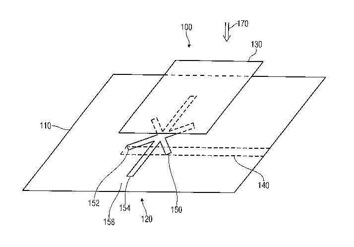
Fig. 1 shows a tilted image of an inventive antenna
structure according to a first embodiment of the present
invention. The antenna structure in its entirety is
referred to by 100. The antenna structure 100 includes a
ground area 110 domprising ari aperture 120. In addition,
the antenna structure includes a radiation electrode 130
arranged above the ground area 110. A feeding line 140
which is shown here as a conducting strip is arranged below
the ground area 110. The aperture 120 includes a first slot
150, a second slot 152 and a third slot 154. The first,
second and third slots 150, 152, 154 each have a
CA 02601530 2007-09-07
- 16 -
rectangular shape and represent an opening of the ground
area 110. The first slot 150 and the second slot 152 are
arranged so as to form a cross. The lengths of the first
slot 150 and the second slot 152 in the embodiment shown
are equal. The third slot 154 is longer than the first slot
150 and the second slot 152 and intersects the first and
second slots 150, 152 in the region in which the first and
second slots 150, 152 also intersect, i.e. in the center of
the cross formed by the first and second slots. In
addition, it is to be pointed out that the third slot 154
in a top view, along a direction shown by an arrow 170, is
perpendicular to the feed line 140. Furthermore, the
aperture 120 comprises a high degree of symmetry. The
geometrical centers of the first, second and third slots
150, 152, 154, except for manufacturing tolerances,
coincide. In addition, there is axis symmetry of the
aperture relative to an axis 158 of the third slot 154. In
addition, the aperture 120 is arranged relative to the feed
line 140 such that the ieed line 140, in top view, passes
through the region in which the first, second and third
slots 150, 152, 154 intersect.
The radiation electrode 130 is a planar conductive
electrode which may also be referred to as patch. In the
embodiment shown i-t is arranged above the aperture 120. The
radiation electrode 130 shown is basically rectangular. The
radiation electrode 130 is implemented to allow a
circularly polarized electromagnetic wave to be radiated.
In the embodiment shown, the radiation electrode is nearly
squared. However, it is also possible to use a rectangular
radiation electrode in which at least one corner is
bevelled and/or cut off. Also, a radiation electrode
comprising a slot in the center which allows circular
polarization can be used. Finally, different geometries may
be used. as long as it is ensured that they allow circular
polarizacion. The radiation electrode 130 is arranged such
that the aperture 120, in a top view, along a direction
CA 02601530 2007-09-07
- 17 -
characterized by the arrow 170 is symmetrical below the
radiation electrode 130.
Furthermore, it is to be pointed out that, all in all, the
wave guide and the radiation electrode are arranged such
that energy from the wave guide can be coupled through the
aperture to the radiation electrode (patch).
The mode of functioning of the present antenna structure
can be described easily. The aperture 120 forms an
inventive resonant cross-aperture. The first slot 150 and
the second slot 152 form a slot in the shape of a cross.
The slots are dimensioned such that no resonance of the
cross-shaped slot occurs in the operating frequency range
of the antenna. Thus, it is achieved that an oscillation
resulting in a circularly polarized electromagnetic wave to
be radiated is excited on the radiation electrode. The
cross-shaped form of the first and second slots 150, 152 of
the aperture 120 contributes to exciting a suitable mixed
vibrational mode allowing such a circular polarization of
the waves radiated. The third slot 154 is operated close to
its resonance so that it contributes to improving the
matching of the antenna described. As is shown, the third
slot 154 is typically longer than the first and second
slots 150, 152, wherein the slot 154 is operated closer to
resonance that the first and second slots. Furthermore, it
is to be pointed out that it is amazing that the third slot
154 does not interfere in the circular polarization of the
electromagnetic wave radiated, as might be expected
according to conventional theories.
The geometry shown can be changed in a wide range without
deviating from the central ideas of the present invention.
Exemplarily, lengths of the three slots 150, 152, 154 which
form the aperture 120 can be altered. Exemplarily, the
length of the third slot 154 can be increased or reduced.
In addition, it is not necessary for the first slot 150 and
the second slot 152 to have the same length. Rather, the
CA 02601530 2007-09-07
- 18 -
lengths of the slots 150, 152, 154 relative to one another
can be changed to allow fine adjustments of the inventive
antenna structure. It is furthermore also possible to
deviate from the strict symmetry of the aperture. This may,
for example, be useful wnen the radiation electrode 130 has
no complete symmetry either. With regard to the angles
between the slots and between a slot and the feed line,
alterations may also be made. Rotation of the slots by up
to 20 degrees is possible to allow fine tuning of the
antenna structure. Thus, the angle between the first slot
and the second slot can deviate from a riaht angle by up to
degrees. This is similarly also true for the angle
between the third slot and the feed line.
15 The radiation electrode 130 can be changed over a wide
range. It may, for example, be rectangular or nearly
rectangular. It is preferred to use a radiation electrode
which is nearly squared, wherein the dimensions and/or edge
lengths differ slightly. Such a radiation electrode allows
20 a circularly polarized electromagnetic wave to be radiated.
Preferably, it is also possible to use a radiation
electrode which has a nearly rectangular or squared shape,
wherein at least one corner is bevelled. In this case, it
is also preferred for reasons of symmetry to bevel two
opposite corners. Finally, a radiation electrode which
comprises a slot in the center can be used, wherein the
slot thus is impl'emented such that a circularly polarized
wave can be radiated. Conventional extensions are possible,
like, for example, coupling additional metallic elements to
the radiation electrode 130. In addition, parasitic
elements, of, for example, a capacitive, conductive or
resistive type, can be coupled to the radiation electrode
130. Thus, a desired mode forming can be forced. Apart from
that, the bandwidth of the antenna can be improved by
parasitic elements. Finally, it is possible to cut off
and/or bevel corners of the radiation electrode 130. The
result is coupling of different vibrational modes between
the radiation electrode 130 and the ground area 110. As a
CA 02601530 2007-09-07
- 19 -
consequence, a suitable phase shift is made between the
different modes so that a right-hand circular polarization
or left-hand one can be set. In addition, the radiation
electrode may also be altered differently, exemplarily by
adding slots to the radiation electrode which suppress
undesired modes or provide for a suitable phase relation
between the desired modes.
Feeding the antenna structure shown can take place in
different ways. The metallic strip conductor 140 shown here
can be replaced by different wave guides. Exemplarily,
these wave guides may be a microstrip line. In addition, a
coplanar wave guide can be used. Additionally, electrical
energy can also be fed by a strip line, a dielectric wave
guide or a cavity wave guide.
Additionally, it is pointed out that Fig. 1 merely
represents a schematical illustration of the basic
structure of an inventive antenna. Characteristics which
are not essential for the antenna are not illustrated here.
Thus, it is to be pointed out that the metallic structures
shown, in particular the ground area 110, the radiation
electrode 130 and the strip line 140, are typically
supported by dielectric materials. It is possible to
introduce nearly any layers or structures of dielectric
materials into the antenna structure 100 shown. Structures
of this kind may, for example, be layers parallel to the
ground area 110. The conducting structures may be deposited
on these dielectric layers and may have been patterned by a
suitable method, exemplarily an etching method. The only
prerequisite here is that the dielectric constant of a
dielectric layer be not too large since this increases
losses resulting in the antenna structure, and radiation is
deteriorated. In addition, when introducing dielectric
structures, it must be kept in mind that no surface waves
should be excited, since they, too, also deteriorate the
radiation efficiency of an antenna structure considerably.
CA 02601530 2007-09-07
- 20 -
A dielectric layer may, for example, be arranged between
the ground area 110 and the strip conductor 140, the result
being a microstrip line. Such a microstrip line is of
particular advantage for coupling an inventive antenna
structure described. In addition, a microstrip line can
also be combined particularly well with active and passive
circuit structures.
Dielectric structures of different shapes are also possible
apart from planar dielectric structures. Exemplarily, the
radiation electrode 130 can be supported by a spacer made
of a dielectric material. Such a design improves the
mechanical stability of the inventive aritenna and allows
cheap manufacturing.
A combination of dielectric layers and layers of very low
dielectric constant, such as, for example, air layers, is
also possible. Air layers reduce electrical losses and may
reduce surface waves excited.
Fig. 2 shows a tilted image of an inventive radiator
geometry according to a second embodiment of the present
invention. The radiator geometry in its entirety is
referred to by 200. It is pointed out that in Figs. 1 and 2
and also in the remaining figures, same reference numerals
refer to same means. A ground area 110 comprising an
aperture 120 is shown here. Specific details of the
aperture are not shown here for reasons of clarity, however
the aperture corresponds to the one described and shown in
Fig. 1. Additionally, the inventive radiator geometry 200
includes a first radiation electrode 130. The aperture 120
represents an opening in the ground area 110 which in a top
view along a direction characterized by the arrow 210 is
below the first radiation electrode 130. A second radiation
electrode 220 is arranged above the first radiation
electrod.e. Tt is enclosed by the third radiation electrode
230, wherein there is a gap 240 between the second
radiation electrode 220 and the third radiation electrode
CA 02601530 2007-09-07
- 21 -
230. The second radiation electrode 220 is connected to the
third radiation electrode 230 via four conductive lands
250, 252, 254, 256. These lands in the implementation shown
are arranged roughly in the center of the edges of the
second radiation electrode 220. The second radiation
electrode 220 is thus arranged such that the first
radiation electrode 130 is between the second radiation
electrode 220 and the ground area 110. In the embodiment
shown, the second radiation electrode 220 and the third
radiation electrode 230 additionally are in a common plane.
Furthermore, the dimensions of the second radiation
electrode 220 differ only slightly from the dimensions of
the first radiation electrode 130. Preferably, the
deviation is less than 20%.
Based on the structural description, the mode of
functioning of an inventive radiator geometry will be
explained in greater detail below. It is pointed out that
such a geometry allows setting up circularly polarized
dual- and/or multiband antennas. The individual layers can
be supported by different boards. Exemplarily, a first
board of a dielectric material can support the ground area
110, whereas a second board supports the first radiation
electrode 130 and a third board supports the second
radiation electrode 220 and the third radiation electrode
230. The boards, however, are not shown here for reasons of
clarity, but may be arranged such that the respective
radiation electrodes are supported by any board surface. At
the bottom of a printed circuit board supporting the ground
area 110, there may be a microstrip line from which power
is transferred through the aperture 120 in the ground area
first to a smaller patch formed by the first radiation
electrode 130. The smaller patch formed by the first
radiation electrode 130 is designed for the upper frequency
band of two frequency bands. The power coupled by the
aperture can subsequently be coupled onto a larger patch
which is designed for the lower one of two frequency bands.
The larger patch effectively includes two patches which in
CA 02601530 2007-09-07
- 22 -
the embodiment shown are formed by the second radiation
electrode 220 and the third radiation electrode 230. The
larger patch here may be interpreted as two patches within
each other having short circuits. The inner smaller patch
formed by the second radiation electrode 220 is
approximately as large as the bottom smaller patch formed
by the tirst radiation electrode 130. Conductive connection
lands 250, 252, 254, 256 connect the second radiation
electrode 220 and the third radiation electrode 230.
Depending on their positions, the connecting lands 250,
252, 254, 256 act on the second radiation electrode and the
third radiation electrode as capacitive or inductive load
and/or coupling, thereby having an effect on the resonant
frequency of the upper radiator formed by the second
radiation electrode 220 and the third radiation electrode
230. A change in the position of a connecting land 250,
252, 254, 256 (relative to the second and third radiation
electrodes 220, 230 and relative to the remaining
connective lands) can thus be used for fine tuning of the
antenna structure. Exemplarily, it is possible to move the
connecting lands 250, 252, 254, 256 from the center of the
edges of the second radiation electrode 220 towards the
corners of the second radiation electrode 220. In case two
corners of the second radiation electrode 220 are bevelled,
it has proven to be of advantage to move the connecting
lands 250, 252, 254, 256 towards these bevelled and/or cut
corners. In addition, it is to be pointed out that the
connecting lands need not be arranged in a strictly
symmetrical manner. Rather, it is practical to arrange the
connecting lands 250, 252, 254, 256 at opposite edges of
the second radiation electrode slightly offset so that a
connecting line between two opposite connecting lands 250,
252, 254, 256 is not parallel to an edge of the second
radiation electrode. Particularly great freedom when fine
tuning the upper radiator results from such an asymmetrical
arrangement. Finally, it should be pointed out that the
connectirig lands may also be omitted when there is
CA 02601530 2007-09-07
- 23 -
sufficient near-field coupling between the second radiation
electrode 220 and the third radiation electrode 230.
The inventive structure thus effectively includes two
radiative structures, namely a so-called lower patch which
is formed by the first radiation electrode 130 and is
particularly effective at higher frequencies, and an upper,
larger patch which is formed by the second radiation
electrode 220 and the third radiation electrode 230.
It is additionally to be pointed out that the distance
between the small patch formed by the first radiation
electrode 130 and the ground area is smaller than the
distance between the second larger patch formed by the
second radiation electrode 220 and the third radiation
electrode 230, and the ground area 110.
An inventive structure offers considerable advantages
compared to known structures, wherein a circularly
polarized radiation can be achieved in two frequency bands
without considerably influencing the purity of polarization
or without exciting surface waves to a greater extent.
It is pointed out here that generally an increase in an
electrical substrate thickness results in higher-order
surface waves forming. When surface waves of this kind
form, the antenna gain is reduced strongly. In order to
avoid and/or keep low the formation of surface waves, the
two antenna structures contained in an inventive geometry
have different effective substrate thicknesses for
different frequency ranges. At lower frequencies, the
upper, larger patch formed by the second radiation
electrode 220 and the third radiation electrode 230 is
effective. The effective substrate thickness equals the
distance of the second and third radiation electrodes from
the ground area 110. This distance is indicated here by D.
However, at higher frequencies, the lower, small patch
formed by the first radiation electrode 130 becomes
CA 02601530 2007-09-07
- 24 -
effective. The effective substrate thickness equals the
distance between the first radiation electrode 130 and the
ground area 110 which is indicated here by d.
It shows that the effective substrate thickness for low
frequencies referred to by D is larger than the effective
substrate thickness for higher frequencies referred to by
d. This corresponds to the requirement that antennas for
different frequencies must have different substrate
thicknesses. Due to the fact that the radiators effective
at different frequencies are in different planes and in
different distances to the ground area 110, the generation
of surface waves is reduced effectively. The very
requirement that the effective substrate thickness be
smaller for high frequencies than for low frequencies is
met.
In addition, the requirement that the antenna for the upper
frequency band (formed by the first radiation electrode
130) must be closer to the ground area 110 and to the
aperture 120 than the antenna for the lower frequency band
(formed by the second radiation electrode 220 and the third
radiation. electrode 230) is met by means of the inventive
geometry. If the larger patch were at the bottom (i.e.
close to the aperture) and the smaller patch at the top
(i.e. remote from the aperture), this would result in poor
polarization charac-ceristics in the upper frequency range,
since the aperture would be shielded by the larger patch.
In such a case, effective coupling of the small patch
through the aperture would not longer be possible.
Correspondingly, a smaller patch separated from the
aperture by a larger patch would not be able to radiate a
circularly polariz,ed wave with a low portion of orthogonal
polarization.
In addition, it is avoided by the inventive geometry in
which the larger patch is composed of two parts, namely the
second radiation electrode 220 and the third radiation
CA 02601530 2007-09-07
- 25 -
electrode 230, that the radiation of the bottom smaller
patch is shielded too strongly by the upper larger patch.
When the antenna for the upper frequency band is closer to
the ground area 110 than the antenna for the lower
frequencv band, the strong shielding of the small radiator
by the large one should be avoided.
Reduced shielding of the radiation of the lower patch 130
by the upper patch 220, 230 is achieved by the gap 140
between the second radiation electrode 220 and the third
radiation electrode 230.
The inventive radiator geometry 200 can also be changed
considerably. All the alterations described before can be
applied to the individual radiation electrodes 130, 220,
230. Exemplarily, it is of advantage to cut the corners of
the corresponding radiation electrodes. Several modes
required for circular radiation can be coupled, while
undesired modes can be suppressed.
Fig. 3 shows a tilted image of an inventive antenna
structure according to a third embodiment of the present
invention. The antenna structure in its entirety is
referred to by 300. It basically corresponds to the antenna
structure 100 shown referring to Fig. 1, so that same means
and geometry characteristics here are provided with same
reference numerals. Unchanged characteristics will not be
described again. However, it is pointed out that in the
antenna arrangement 300 a first corner 310 and a second
corner 320 of the first radiation electrode 130 are cut off
and/or bevelled. This geometrical alteration contributes to
the fact that a circularly polarized electromagnetic wave
can be radiated. In addition, the antenna arrangement 300
comprises a stub 330 applied to the strip line 140. This
stub 330 serves further impedance matching of the present
antenna structure. The dimensioning of such a stub for
matching is known to one skilled in the art.
CA 02601530 2007-09-07
- 26 -
In addition, Fig. 3 shows an enclosing cuboid 340 enclosing
the entire antenna structure. Such an enciosing cuboid may,
for example, be us.ed to delineate a simulation region in an
electromagnetic simulation of an antenna structure.
Fig. 4 shows a tilted image of an inventive antenna
structure according to a fourth embodiment of the present
invention. The antenna structure in its entirety is
referred to by 400. The antenna structure 400 includes a
feed line 140, a ground area 110 having an aperture 120,
and a first radiation electrode 130, a second radiation
electrode 220 and a third radiation electrode 230. The
geometry of the firs'.:~ radiation electrode 130 here
basically corresponds to the geometry of the first
radiation electrode 130 shown in Fig. 3. The second and
third radiation electrodes 220, 230 are basically arranged
as is described referring to Fig. 2. However, in the
antenna structure 400, two opposite corners 410, 420 of the
second radiation -electrode 220 are bevelled. The third
radiation electrode 230 in turn encloses the second
radiation electrode 220, wherein there is a slot and/or gap
240 between the second radiation electrode 220 and the
third radiation electrode 230. Additionally, it is to be
pointed out that the third radiation electrode 230 in its
shape is adjusted to the second radiation electrode 220.
This means that the third radiation electrode 230 is
adjusted to the bevelled corners 410, 420 of the second
radiation electrode 220 such that the gap 240 between the
second radiation electiode 220 and the third radiation
electrode 230 basically has an equal width also in the
region of the bevelled corners 410, 420. The inner edges of
the third radiation electrode 230 thus are basically
parallel to the external edges of the second radiation
electrode 220. The third radiation electrode 230, too,
comprises two external bevelled corners 430, 440 which are
adjacent to the bevelled corners 410, 420 of the second
radiation electrode 220. Thus, both the first, second and
third radiation electrodes 130, 220, 230 comprise bevelled
CA 02601530 2007-09-07
- 27 -
corners 310, 320, 410, 420, 430, 440, wherein the
respective adjacent corners of the different radiation
electrodes are bevelled. The second and third radiation
electrodes 220, 230 are coupled via connecting lands 250,
252, 254, 256, wherein the connective lands 250, 252, 254,
256 are arranged roughly in the center of edges of a
rectangle representiing the second radiation electrode 220,
except for the bevelled corners.
In addition, it is pointed out that the size of the second
radiation electrode 220, except for a deviation of at most
20%, equals the size of the first radiation electrode 130.
As to the shape, too, the first and second radiation
electrodes 130, 220 do not differ considerably. Thus, they
are nearly parallel electrodes of nearly equal shape having
nearly the same dimensions.
The layer sequence is explicitly pointed out here again.
The feed line 140 forms the bottommost conducting layer. A
ground area 110 comprising an aperture 120 is arranged
above it. The first radiation electrode 130 is arranged
above this in one plane. The second radiation electrode 220
and the third radiation electrode 230 are arranged in
another plane further up. The respective metallizations,
i.e. the feed line 140, the ground area 110 and the first,
second and third radiation electrodes 130, 220, 230, are
each supported by dielectric layers.
Additionally, it is mentioned here that the width of the
feed line 140 is changed for adjusting purposes. The feed
line 140, away from the aperture, has a broad portion 450,
whereas the feed line 140 is narrower close to the
aperture. A narrow feed line is of advantage since it
causes a greater concentration of the electrical field.
Thus, a stronger coupling of the radiation elecirodes can
occur Lo the feed line through the aperture 120.
Furthermore, the change in the width of the feed line also
serves impedance matc!iing, wherein matching can be
CA 02601530 2007-09-07
- 28 -
influenced by suitably choosing the length of the thin
piece 460.
Also shown is an enclosing rectangle 470 which delineates a
simulation region in which the antenna structure is
simulated. The enclosing rectangle also indicates the
thickness of the respective layers.
Fig. 5 shows a photograph of an inventive planar antenna
structure prototype according to a third embodiment of the
present invention. A constructed monoband antenna is shown
here, designed for the frequency range from 2.40 GHz to
2.48 GHz. The antenna in its entirety is referred to by
500. It comprises a first board 510 made of a dielectric
material and a second board 520 made of a dielectric
material. The two boards are separated and/or fixed by four
spacers 530 made of a dielectric material. The first
dielectric board 510 supports a first radiation electrode
130. The second dielectric board 520 supports, on an upper
area, the ground area 110 comprising an aperture 120. The
lower side of the dielectric board 530 supports a feed line
via which electrical energy is fed to the antenna from an
SMA socket 550.
The antenna arrangement 500 has a first dimension 570 of 75
mm which can be taken as a width. A second dimension 572
which can be taken as a length is also 75 mm. Finally, a
third dimension 574 which can be taken as a height is
10 mm. ~. ast for size comparison purposes, a one Euro coin
576 is shown here.
Fig. 6 shows a photograph of a prototype of an inventive
antenna structure according to the fourth embodiment of the
present invention. The antenna structure in its entirety is
referred to by 600. It includes a first dielectric layer
610, a second dielectric layer 620 and a third dielectric
layer 630.
CA 02601530 2007-09-07
- 29 -
The 3 dielectric layers or boards 610, 620, 630 are
supported by dielectric spacers 640. The first dielectric
board 610 here supports a second radiation electrode 220
and a third radiation electrode 230. The second dielectric
board supports a first radiation electrode 130. The third
dielectric board 630 supports a ground area 110 on one side
and a feed line 140 on the other side. The feed line is
also led out to an SMA socket 650. The entire antenna
structure 600 forms a dual-band antenna.
The antenna 600 has a first dimension 670 which can also be
taken as a length. This first dimension is 75 mm. In
additiori, the antenna 600 has a second dimension 672 which
can be taken as a width which is also 75 mm. A third
dimension 674 of the antenna 600 can be taken as a height.
This height is 10.5 mm.
The dual-band antenna 600 shown is based on the monoband
antenna 500, wherein the monoband antenna has been improved
to form a dual-band antenna. The antenna 600 which in its
principle setup corresponds to the antenna 400 shown in
Fig. 4 is set up of several layers which will be discussed
in greater detail below. The bottommost sheet of the
antenna is formed by a patterned conductive layer,
exemplarily a metallization layer and/or metal layer which
as a whole forms a microstrip line. This microstrip line is
deposited on the bottom side of a first substrate of the
type FR4, wherein the first substrate has a thickness of
0.5 mm. The first substrate corresponds to the third
dielectric layer 630. A ground area having an overall
extension of 75 mm x 75 mm is deposited on the top of the
first substrate. The ground area additionally includes an
aperture 120. A layer which is not filled by a dielectric
material is arranged above the ground area.
Correspondingly, the antenna also includes an air layer
having a thickness of 5 mm. Another conductive layer on
which the first radiation electrode is formed as a patch is
arranged above this air layer. The further conductive layer
CA 02601530 2007-09-07
- 30 -
is supported by a second dielectric layer made of FR4 which
again has a thickness of 0.5 mm. The second dielectric FR4
layer corresponds to the second dielectric layer 620 shown
in Fig. 6. A layer in which there is no solid dielectric is
arranged above the second dielectric FR4 layer. The result
is a second air layer the thickness of which is 4 mm. A
third dielectric FR4 layer having a thickness of 0.5 mm is
arranged above it.. The third dielectric FR4 layer supports
another conductive layer on which the second radiation
electrode and the third radiation electrode in the form of
patches are formed by patterning. Conducting connecting
lands between the second radiation electrode and the third
radiation electrode have a width of 1 mm. The entire
antenna structure thus includes the following layers in the
order shown: microstrip line; FR4 (0.5 mm); ground area (75
mm x 75 mm, including aperture); air (5 mm); patch 1 (first
radiation electrode); FR4 (0.5 mm); air (4 mm); FR4 (0.5
mm) and patch 2(seco-nd radiation electrode and third
radiation electrode). All the layers and dimensions can be
varied by up to 30%. However, it is preferred for the
deviation from the preferred dimensions not to be more than
150.
Fig. 7 shows a graphical illl_istration of the form of the
reflection coefficient S11 for a prototype 500 of an
inventive antenna according to a third embodiment of the
present invention. The graphical illustration in its
entirety is referred to by 700. The input reflection factor
Sil has been measured for a constructed patch antenna which
is designed for a frequency range from 2.40 to 2.48 GHz. A
photograph of such an antenna 500 is shown in Fig. 5.
The frequency of 2.15 GHz to 2.85 GHz is plotted on the
abscissa 710. The ordin.a~.e 712 shows, in logarithmic style,
the magnitude of the input reflection factor S11. Here, the
input reflection factor is plotted in a range from -50 dB
to 0 dB. A first graph 720 shows a simulated input
reflection factor. A second graph 730 shows the measured
CA 02601530 2007-09-07
- 31 -
value for the input reflection factor. According to the
measurement, the input reflection factor is below -10 dB in
the entire frequency range shown from 2.15 GHz to 2.85 GHz.
The simulation, too, shows a similar broadband
characteristic of the antenna.
Fig. 8 shows a graphical illustration of the polarization
decoupling for a prototype 500 of an inventive antenna
according to the third embodiment of the present invention.
The graphical illustration in its entirety is referred to
by 800. The frequency in a range from 2.3 GHz to 2.55 GHz
is plotted on the abscissa 810. The ordinate 812 shows the
polarization decoupling in decibels in a range between 0
and 25 dB. A first graph 820 shows a simulated form of the
polarization decoupling, whereas a second graph 830 shows
the measured values. In the bandwidth required of 2.40 GHz
to 2.48 GHz, the cross-polarization, with a sufficient
adjusting factor, is suppressed by more than 15.5 dB.
Fig. 9 shows a graphical illustration of the form of the
reflection coefficient Sll for a prototype 600 of an
inventive antenna according to the fourth embodiment of the
present invention. The graphical illustration in its
entirety is referred to by 900. Measuring results are shown
here for the reflection coefficient of an inventive dual-
band antenna, as has been described referring to Figs. 4
and 6. The abscissa 910 here shows the frequency range
between 2 GHz and 6 GHz. The magnitude of the input
reflection factor Sll in logarithmic style is plotted on
the ordinate 912 from -40 dB to +40 dB. A graph 920 shows
the form of the input reflection factor relative to
frequency. Also shown are a first marker 930, a second
marker 932, a third marker 934 and a fourth marker 936. The
first marker shows that the input reflection factor at
2.40 GHz is -13.618 dB. The second marker shows an input
reflection factor of -16.147 dB at 2.48 GHz. The third
marker shows an input reflection factor of -9.457 dB at
5.15 GHz, and the fourth marker shows an input reflection
CA 02601530 2007-09-07
- 32 -
factor of -10.011 dB at 5.35 GHz. The fifth marker finally
shows an input reflection factor of -0.748 dB at
4.0008 GHz.
It shows that the input reflection factor in the ISM band
between 2.40 GHz and 2.48 GHz is less than -13 dB and that
the input reflection factor in the ISM band between 5.15
GHz and 5.35 GHz is less than -9.4 dB.
Apart from the input reflection factor, the radiation
characteristics of the dual-band antenna were also
measured. In the ISM band between 2.40 GHz and 2.48 GHz,
the antenna gain of a prototype of a dual-band antenna is
between 7.9 dBic and 8.3 dBic. The half-width is here 70
and the polarization decoupling is between 11 dB and 22 dB.
In the ISM band between 5.15 GHz and 5.35 GHz, the antenna
gain is between 5.9 dBic and 7.3 dBic. The half-width is
35 , the polarization decoupling is between 5 dB and 7 dB.
The adjusting characteristics and radiation characteristics
required can be achieved by an inventive dual-band antenna.
Furthermore, it is to be mentioned that the polarization
purity for the upper frequency range can still be
optimized. Geometrical details may, for example, be
altered.
In summary, it can be stated that the present invention
provides a planar circularly polarized antenna which may be
used in the ISM bands of 2.40 GHz to 2.48 GHz and 5.15 GHz
to 5.35 GHz. The suggested shape of the slot for an
aperture-coupled patch antenna allows radiating nearly
purely circularly polarized waves at a relatively large
bandwidth of the reflection coefficient Sll. This is in
particular also possible for multiband antennas. A radio
link can be achieved by an inventive antenna, wherein the
intensitV of the signal received by an inventive antenna at
a linear polarization of a transmitter is independent of
CA 02601530 2007-09-07
- 33 -
the insertion position of the receive antenna. Put
differently, a linearly polarized signal can be received by
a circl.ilarly polarized antenna, independently of the
orientation of the antenna.
The inventive antenna has been developed in several steps.
A first sub-task was developing an aperture-coupled antenna
for a frequency range of 2.40 to 2.48 GHz having a right-
hand circular polarization (RHCP). In simulation, it has
been paid attention to that a strong suppression of the
orthogonal polarization within the bandwidth necessary is
achieved. Thus, it has been found out that cross-
polarization is suppressed strongly when feeding a patch
through a non-resonant cross-aperture. However, in such a
non-resoriant cross-aperture, the bandwidth of the
reflection coefficient is narrow. A resonant rectangular
aperture (so-called SSFIP principle) comprises a larger
bandwidth, wherein, however, polarization decoupling is
weaker. Finally, a combination of the two slot geometries
not known before has proven to be of advantage, which is
here referred -to as resonant cross-aperture. A
corresponding antenna geometry has been shown in Figs. 1, 3
and 5.
Furthermore, it has shown that an inventive geometry shown
of the aperture and/or the slot also allows setting up
circularly polarized dual- and/or multiband antennas. The
concept to be described below may be used here. In the case
of two bands, the antenna includes three boards.
Corresponding arrangements are, for example, shown in Figs.
4 and 6. Ori the bottom side of the bottom printed circuit
board, there is a microstrip line the power of which
couples through an aperture in the ground area first to a
small patch (for the upper frequency band) and then a
larger patch (for the two frequency bands) including two
patches. Thus, the larger patch can be interpreted as "two
patches within each other having short circuits". The inner
CA 02601530 2007-09-07
- 34 -
smaller patch preferably has the same size as the bottom
patch.
A number of problems occurring in conventional antennas can
be solved by such a structure and/or such a dual-band
concept. Increasing the electrical substrate thickness
conventionally results in higher-order surface waves
forming, thereby strongJy reducing the antenna gain. Thus,
the two antennas must have different substrate thicknesses
for different frequency ranges. The antennas for different
frequency ranges consequently have to be in different
planes. This can be achieved by means of an inventive
antenna geometry.
A conventional variation with a larger bottom patch and a
smaller top patch comprises poor polarization
characteristics, since the aperture is shielded by the
larger patch. The antenna for the upper frequency band
consequently has to be closer to ground than the antenna
for the lower frequency band, which can be achieved by an
inventive geometry.
Since the antenna for the upper frequency band thus must be
closer to the ground area than the antenna for the lower
frequency band, strong shielding of the small radiator for
the upper frequency band by the large radiator for the
lower frequency band should be avoided. This can be
achieved by forming the radiator for the lower frequency
band by two radiation electrodes between which there is a
gap.
Adjusting an inventive antenna can be performed by a
transformer and/or a stub.
Compared to conventional antennas, an inventive antenna has
a number of advantages. Feeding an antenna through a
resonant cross slot allows setting up completely planar,
relatively small and cheap antennas. At the same time, high
CA 02601530 2007-09-07
- 35 -
polarization purity and large impedance bandwidth can be
achieved. In addition, planar circularly polarized
multiband antennas can be constructed. Thus, the area
consumption of the entire antenna is determined only by the
size of the antenna element for the lowest frequency.
Compared to broadband antennas, an inventive antenna still
offers better pre-filtering.