Note : Les descriptions sont présentées dans la langue officielle dans laquelle elles ont été soumises.
CA 02601551 2007-09-12
2006P52322 CA 1
A METHOD AND SYSTEM FOR PROVIDING AN INFORMATION FOR RECOVERING
A CLOCK FREQUENCY
BACKGROUND OF THE INVENTION
[0001] The present invention relates to a method of providing
an information for recovering a clock frequency via a data net-
work, a method of providing an information for recovering a
clock frequency to a data network, a method of generating a
value representative of a frequency difference between a clock
frequency and a reference frequency, a system for providing an
information for recovering a clock frequency via a data net-
work, an apparatus for providing an information for recovering
a clock frequency to a data network, and a digital phase-locked
loop.
[0002] In recent years, different types of communication net-
works have been developed to carry various types of informa-
tion. Communication networks typically make use of one of two
well established transmission mechanisms, namely the circuit
switched transfer and the packet switched transfer. The older
networks like telephone networks for voice communication are
primarily circuit switched networks. In a circuit switched net-
work, each call establishes a dedicated point-to-point-
connection through the network which, for instance, allows peo-
ple at both ends of a telephone call to speak and listen at the
same time.
[0003] A circuit remains open for the entire duration of a
call even if no one is speaking, which means that a significant
amount of circuit's bandwidth, or capacity to carry informa-
tion, is wasted on silence, or meaningless data. In order to
utilize the capacity more efficiently, circuit switched tele-
communication networks have made use of time division multi-
plexed (TDM) circuits to interconnect network switches. In TDM,
CA 02601551 2007-09-12
2006P52322 CA 2
analog signals are digitally coded and multiplexed in time over
circuits at a constant bit rate.
[0004] The wide spread use of computers in the last decades
has let to the development of additional types of networks.
These networks have been configured for the purpose of data
communications and are primarily packet switched networks. In a
packet switched network, a call may consist of a stream of data
sent from one computer to another. The stream of data is di-
vided up into packets before it enters the network. At the des-
tination, the stream of data is re-assembled from the packets.
Thus packet switched networks typically do not allocate fixed
resources to transmitters, but rather route packets of data on
a best efforts basis using destination address information con-
tained in packet headers, and network switches and routers.
[0005] A packet switched call therefore does not require a
dedicated connection through the network. Instead, packets from
many different calls can share the same bandwidth. That is,
packets from one call can be inserted into spaces between pack-
ets from other calls. For these reasons, packet switched net-
works efficiently utilize much more network bandwidth than cir-
cuit switched networks, making packet switched networks par-
ticularly suited to handle large volumes of data.
[0006] Packet switched networks are becoming more popular
amongst network operators as they often provide better perform-
ance, and are more cost effective to install and maintain than
equivalent circuit switched networks. Moreover, for the above-
mentioned reasons of performance and cost, many operators and
leased line providers who provide bandwidth to service provid-
ers are moving towards replacing TDM sources with packet net-
works. In many cases, switch to switch communications will be
provided entirely over packet networks. However, it is likely
that for many years to come, some operators will continue to
rely upon TDM circuits to provide all or at least a part of the
CA 02601551 2007-09-12
2006P52322 CA 3
networks. This will bring about a constant need for interwork-
ing methods and systems between packet networks and TDM systems
[0007] Packet switched networks, however, normally do not work
well for time critical transmissions such as voice. For in-
stance, in packet switched networks, packets may experience de-
lay variations while traveling through the network. As a re-
sult, packets are rarely received at a constant bit rate. In
data communications, delay variations between packets usually
do not matter. A computer can just wait for a complete set of
packets to arrive before processing the data. For time critical
transmissions, however, delay variations can have a significant
impact on the quality of the call. In such case, circuit
switched networks like TDM are generally better suited for con-
stant bit rate, time critical transmissions such as voice com-
munication.
[0008] In general, TDM links are synchronized circuits with a
constant (transmission) bit rate governed by a service clock
operating at some pre-defined frequency. In contrast, in a
packet network there is no direct link between the frequency at
which packets are sent from an ingress port of the network and
the frequency at which they arrive at an egress port of the
network. In order to provide a TDM circuit emulation, there
must be provided at the ports of the packet network an inter-
working between the TDM links and the packet network in such a
way that the TDM link at the ingress side is synchronized with
the TDM link at the egress side. That is to say that the TDM
service frequency at the customer premises on the ingress side
must be exactly reproduced at the egress side of the packet
network. The consequence of any long-term mismatch in these
frequencies will be that the queue, for example, in a buffer
memory etc., at the egress of the packet network will either
fill up or empty, depending upon on whether the regenerated
clock is slower or faster than the original clock, causing loss
of data and degradation of the service. Also, unless the phase
CA 02601551 2015-04-02
31489-4
4
of the original clock is tracked by that of the regenerated
clock, a lag in frequency tracking will result in small but
nonetheless undesirable changes to the operating level of the
queue at the egress.
SUMMARY OF THE INVENTION
[0008a] According to one aspect of the present invention,
there is provided a system comprising: a time domain
multiplexing (TDM) transmission entity comprising: a first TDM
transmission system to transmit a TDM bitstream over a
T-carrier or E-carrier line according to a TDM service clock, a
first TDM reception system to receive the TDM bitstream over
the T-carrier or E-carrier line according to the TDM service
clock, and a digital phase-locked loop to generate a digital
value representative of a frequency difference between the TDM
service clock frequency and a reference frequency; and a first
interworking function element to convert the TDM bitstream to a
series of packets and transmit the series of packets over an
asynchronous network along with the generated digital value
according to the reference frequency.
[0008b] According to another aspect of the present invention,
there is provided a method comprising: a first time domain
multiplexing (TDM) transmission entity transmitting a TDM
bitstream over a T-carrier or E-carrier line according to a TDM
service clock; a first TDM reception system receiving the TDM
bitstream over the T-carrier or E-carrier line according to the
TDM service clock; a digital phase-locked loop generating a
digital value representative of a frequency difference between
the TDM service clock frequency and a reference frequency; and
a first interworking function element converting the TDM
bitstream to a series of packets and transmitting the series of
CA 02601551 2015-04-02
31489-4
4a
packets over an asynchronous network along with the generated
digital value according to the reference frequency.
BRIEF DESCRIPTION OF THE SEVERAL VIEWS OF THE DRAWINGS
[0009] Embodiments of the invention are better understood
with reference to the following drawings.
Fig. 1 is a block diagram for illustrating an embodiment of an
apparatus according to the present invention;
Fig. 2 is a block diagram for illustrating an embodiment of a
system according to the present invention;
Fig. 3 is a block diagram for illustrating an embodiment of a
digital phase-locked loop according to the present invention;
Fig. 4 is a block diagram for illustrating a further embodiment
of an apparatus according to the present invention and a
digital phase-locked loop according to the present invention;
Fig. 5 is a block diagram for illustrating a further embodiment
of an apparatus and a digital phase-locked loop according to
the present invention;
Fig. 6 is a block diagram for illustrating a further embodiment
of a system according to the present invention;
Fig. 7 is a block diagram for illustrating a further embodiment
of a system according to the present invention.
DETAILED DESCRIPTION OF EMBODIMENTS
CA 02601551 2007-09-12
2006P52322 CA 5
[0010] Embodiments of the invention are described with refer-
ence to the drawings, wherein like reference numerals are gen-
erally utilized to refer to like elements throughout. In the
following description for purposes of explanation, numerous
specific details are set forth in order to provide a thorough
understanding of one or more aspects of embodiments of the in-
vention. It may be evident, however, to one skilled in the art
=
that one or more aspects of the embodiments of the invention
may be practiced with a lesser degree of the specific details.
In other instances, known structures and devices are shown in
block diagram form in order to facilitate describing one or
more aspects of the embodiments of the invention. The following
description is therefore not to be taken in a limiting sense,
and the scope of the invention is defined by the appended
claims.
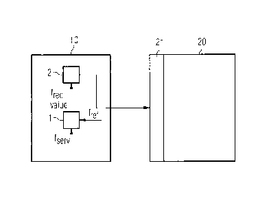
[0011] Referring to Fig. 1 there is shown a block diagram for
illustrating an embodiment of an apparatus according to the
present invention. The apparatus comprises a digital phase-
locked loop 1 which is integrated within the environment of a
transmission entity 10, for example, at a customer premises.
The transmission entity 10 can be, for example, a TDM transmis-
sion entity. The digital phase-locked loop 1 comprises a first
input for receiving a first signal having a clock frequency
fserv which is the service clock frequency of the TDM transmis-
sion entity 10, and a second input for receiving a second sig-
nal having a reference frequency fref. The digital phase-locked
loop 1 generates a value, in particular a digital value, repre-
sentative of a frequency difference between the clock frequency
fserv and the reference frequency fref. The apparatus also com-
prises a transmitting device 2 for transmitting the generated
value to an ingress interface 21 of a data network 20. The
transmitting device 2 may, for example, transmit the generated
value to connection lines which connect the transmitting device
2 with an output port of the transmission entity 10 and the
output port of the transmission entity 10 with the ingress in-
CA 02601551 2007-09-12
2006P52322 CA 6
terface 21 of the data network 20. The transmitting device 2
may, for example, also serve for transmitting TDM data like
e.g. payload data from the transmission entity 10 to the data
network 20 and as well the connection lines may, for example,
be used also for transmitting TDM data like payload data from
the TDM transmission entity 10 to the data network 20. The data
network 20 can be, for example, a packet switched network.
[0012] Referring to Fig. 2, there is shown a block diagram for
illustrating an embodiment of a system according to the present
invention. The system comprises a digital phase-locked loop 1
integrated within the environment of a TDM transmission entity
10. As already described in connection with Fig. 1, the digital
phase-locked loop 1 generates a value representative of a fre-
quency difference between a clock frequency fserv and a refer-
ence frequency fref and transmitting device 2 to transmit the
generated value to an ingress interface 21 of a data network
20. The system further comprises a recovering device 31 inte-
grated within the environment of a reception entity 30 wherein
the recovering devices 31 are coupled to an egress interface 22
of the data network 20. The recovering devices 31 comprise a
first input for inputting the reference frequency fref and a
second input coupled to the egress interface 22 of the data
network 20. In the recovering device 31, the clock frequency
fserv is recovered by use of the supplied reference frequency
fref and the transmitted value which is representative of the
frequency difference between the clock frequency fserv and the
reference frequency fref. The reception entity 30 can be, for
example, a TDM reception entity. The interfaces 21 and 22 may
comprise interworking function blocks that provide for rate ad-
aptation and protocol conversion.
[0013] Referring to Fig. 3, there is shown a block diagram for
illustrating an embodiment of a digital phase-locked loop ac-
cording to the present invention. The digital phase-locked loop
1 comprises a proportional-integral (PI) loop filter 1.1 and an
CA 02601551 2007-09-12
2006P52322 CA 7
output 1.2, coupled to the PI loop filter 1.1, for outputting
an integral term of the loop filter 1.1. In another embodiment,
instead of using a PI loop filter 1.1 a proportional-integral-
differential (PID) loop filter 1.1 may be used.
[0014] Referring to Fig. 4, there is shown a block diagram for
illustrating an apparatus according to a further embodiment of
the present invention and a digital phase-locked loop according
to the present invention. The digital phase-locked loop 100 as
shown in Fig. 4 comprises a phase detector 110, a proportional-
integral (PI) loop filter 120 and a digitally controlled oscil-
lator (DCO) 130. The phase detector 110 comprises two inputs
for inputting the service clock frequency fserv and the output
frequency fpll of the digital phase-locked loop 100. An output
of the phase detector 110 is coupled to an input of the PI loop
filter 120. The PI loop filter 120 comprises a proportional
part and an integral part wherein the output signal of the
phase detector 110 is supplied to both the proportional part
and the integral part. The proportional part comprises a first
multiplier 121 and the integral part comprises a second multi-
plier 123, a first adder 124 and a regulator 125. The output
signal of the phase detector 110 is supplied to the first mul-
tiplier 121 where it is multiplied with a value Kp. The output
signal of the first multiplier 121 is supplied to the first in-
put of a second adder 122. The output signal of the phase de-
tector 110 is also supplied to the second multiplier 123 where
it is multiplied with a value Ki. The output of the second mul-
tiplier 123 is supplied to a first input of the first adder
124. The output of the first adder 124 is supplied to the sec-
ond input of the second adder 122. The output of the first ad-
der 124 is also supplied to the input of the regulator 125 and
the output of the regulator 125 is supplied to the second input
of the first adder 124. An output signal sfout of the PI loop
filter 120, which is an output signal of the second adder 122,
is supplied to a first input of a third adder 126 and a nominal
increment is supplied to a second input of the third adder 126.
CA 02601551 2007-09-12
2006P52322 CA 8
An output of the third adder 126 is supplied to an input of the
DCO 130.
[0015] In operation, the digital phase-locked loop 100 will be-
come synchronized to the service clock frequency fserv as set
forth below. In an unlocked state of the digital PLL 100 the
output frequency fpll will be designated as fservnom. This fre-
quency is derived directly from the reference frequency fref
supplied to the DCO 130. In a locked state of the digital PLL
100 the output of the DCO 130 will be the synchronized service
clock frequency fservsync wherein fservsync = fserv. The fre-
quency difference between fservnom and fserv can be derived
from the integral term of the PI loop filter 120. The thus de-
termined difference information which is a digital value is
transmitted via the data network and can be used on the egress
entity of the data network to recover the service clock fre-
quency fserv on the basis of the reference frequency fref which
is available on both sides on the data network.
[0016] When using a DCO 130 for the generation of the output
frequency within the digital PLL 100 the frequency of the free
running DCO 130 must be in synchronism with the reference fre-
quency fref. If the output signal sfout = 0 then the output
frequency of the PLL 100 is fservnom which is in synchronism
with the reference frequency fref.
[0017] Referring to Fig. 5, there is shown a block diagram for
illustrating a further embodiment of an apparatus according to
the present invention and a digital phase-locked loop according
to the present invention. Digital PLL 200 is identical with the
PLL as depicted in Fig. 4 besides that the DCO 130 of the digi-
tal PLL 100 of Fig. 4 is replaced by a frequency synthesizer
135 in the digital PLL 200 as depicted in Fig. 5. The frequency
synthesizer 135 comprises a sigma-delta-modulator 136 and is
constructed in the same way as disclosed in the International
(PCT) Patent Application No. PCT/DE99/03580, Publication No. WO
CA 02601551 2011-12-12
30756-2
9
00/28666. The frequency synthesizer 135 which is based on the
sigma-delta-modulator 136 is used to generate the output fre-
quency fpll of the digital PLL 200 which in operation will be-
come synchronized to the service clock frequency fserv.
[0018] Referring to Fig. 6, there is shown a block diagram for
illustrating a further embodiment of a system according of the
present invention. A TDM bit stream is supplied to a TDM trans-
mission system which is connected to a digital phase-locked
loop (PLL) 1. A service clock frequency fserv is supplied to
the digital PLL 1 by the TDM transmission system. A reference
frequency fref is also supplied to the digital PLL 1. The digi-
tal PLL 1 synchronizes to the service clock frequency fserv and
generates a value which corresponds to the frequency difference
between the clock frequency fserv and the reference frequency
fref. The value corresponding to the frequency difference is .
transmitted from the digital PLL 1 to the TDM tk.ansmission sys-
tem. From the TDM transmission system transmission data like
e.g. payload data are transmitted on a transmitting line such
as a Ti/El line to a TDM reception system. On the same trans-
mitting line, the value corresponding to the frequency differ-
ence is also transmitted from the TDM transmission system to
the TDM reception system. The TDM transmission system, the
digital PLL 1, and the TDM reception system form together a TDM
transmission entity 10 as depicted in Figs.1 and 2.
[0019] From the TDM reception system a TDM bit stream is trans-
mitted to a first interworking function block 21.1 which con-
tains hardware and/or software elements that provide a rate ad-
aptation and protocol conversion from the TDM system to the
packet switched network 20. The first interworking function
block 21.1 converts the TDM bit stream into a stream of =data
packets and sends the stream of data packets into the packet
switched network 20 wherein each data packet contains a header
carrying an information about the destination of the respective
CA 02601551 2007-09-12
2006P52322 CA 10
data packet. At the destination entity the data packets are ex-
tracted from the packet switched network 20 and supplied to a
second interworking function block 22.1 which contains hardware
and/or software elements that provide the rate adaptation and
protocol conversion between the packet switched network 20 and
the TDM system. The second interworking function block 22.1
converts the data packets into a TDM bit stream which is output
by a TDM interface coupled to the second interworking function
block 22.1. The second interworking function block 22.1 is cou-
pled to a frequency synthesizer 31.1 which receives the value
corresponding to the frequency difference from the second in-
terworking function block 22.1 and which is also supplied with
the reference frequency fref. The frequency synthesizer 31.1
comprises, for example, a digitally controlled oscillator which
is supplied with the reference frequency fref and the value
corresponding to the frequency difference. The frequency syn-
thesizer 31.1 synchronizes to the service clock frequency fserv
and forwards the same to the second interworking function
block.
[0020] Referring to Fig. 7, there is shown a further embodiment
for illustrating a system according to the present invention.
This embodiment is similar to the embodiment as depicted in
Fig.6 besides the fact that the packet switched network of the
embodiment of Fig.6 is replaced by a Gigabit Passive Optical
Network (GBON) 40. An input of a TDM reception system is cou-
pled with a transmitting line such as a Ti/El line for receiv-
ing a TDM bit stream. The TDM reception system is also coupled
to a digital PLL 1. A service clock frequency fserv is supplied
to the digital PLL 1 by the TDM reception system. A reference
frequency fref is also supplied to the digital PLL 1. The digi-
tal PLL 1 synchronizes to the service clock frequency fserv and
generates a value which corresponds to the frequency difference
between the clock frequency fserv and the reference frequency
fref. The value corresponding to the frequency difference is
transmitted from the digital PLL 1 to a first interworking
CA 02601551 2007-09-12
2006P52322 CA 11
function block 21.1. The reception system and the digital PLL 1
form together a TDM transmission entity 10 as depicted in
Figs.1 and 2.
[0021] A TDM bit stream is transmitted from the TDM reception
system to the first interworking function block 21.1 which con-
tains hardware and/or software elements that provide a rate ad-
aptation and protocol conversion from the TDM system to the
GPON 40. The first interworking function block 21.1 converts
the TDM bit stream into a stream of data packets and sends the
stream of data packets into the GPON 40 wherein each data
packet contains a header carrying an information about the des-
tination of the respective data packet. At the destination en-
tity the data packets are extracted from the GPON 40 and sup-
plied to a second interworking function block 22.1 which con-
tains hardware and/or software elements that provide the rate
adaptation and protocol conversion between the GPON 40 and the
TDM system. The second interworking function block 22.1 con-
verts the data packets into a TDM bit stream which is output by
a TDM interface coupled to the second interworking function
block 22.1. The second interworking function block 22.1 is cou-
pled to a frequency synthesizer 31.1 which receives the value
corresponding to the frequency difference from the second in-
terworking function block 22.1 and which is also supplied with
the reference frequency fref. The reference frequency fref may
be transmitted through the GPON 40, as indicated by the dashed
line. The frequency synthesizer 31.1 comprises, for example, a
digitally controlled oscillator which is supplied with the ref-
erence frequency fref and the value corresponding to the fre-
quency difference. The frequency synthesizer 31.1 synchronizes
to the service clock frequency fserv and forwards the same to
the second interworking function block 22.1.
[0022] Embodiments of the present invention may be used when-
ever data of a synchronous system, in particular TDM data, are
transmitted over an asynchronous packet switched network. The
CA 02601551 2007-09-12
2006P52322 CA 12
value corresponding to the frequency difference can, for exam-
ple, be generated at the source of a communication service such
as a Ti/El service. For this purpose the same digital PLL can
be used which is already present for the generation of the com-
munication clock signal such as a Ti/El transmission clock sig-
nal. Alternatively another digital PLL can be implemented which
is only used for the generation of the value corresponding to
the frequency difference.