Note : Les descriptions sont présentées dans la langue officielle dans laquelle elles ont été soumises.
CA 02601729 2007-09-17
Method for operating a pulsed arc vaporizer source as well as a vacuum process
installation with pulsed arc vaporization source
The invention relates to a vacuum process installation for the surface
treatment of
workpieces with an arc vaporizer source according to the preamble of claim 1
as well as
to a method for operating an arc vaporizer source according to the preamble of
claim 14.
The operation of arc vaporizer sources, also known as spark cathodes, by
feeding with
electrical pulses has already been known in prior art for a relatively long
time. With arc
vaporizer sources high vaporization rates and consequently high deposition
rates can be
economically attained in coating. The structuring of such a source can,
moreover, be
technically relatively easily realized as long as higher requirements are not
made of the
pulse operation and the pulsing is more or less restricted to the ignition of
a DC
discharge. These sources operate at currents typically in the range of
approximately 100
A and more, and at voltages of a few volts to a few tens of volts, which can
be realized
with relatively cost-effective DC power supplies. A significant disadvantage
with these
sources comprises that in the proximity of the cathode spot very rapidly
proceeding
melting occurs on the target surface, whereby drops are formed, so-called
droplets, which
are hurled away as splatters and subsequently condense on the workpiece and
consequently have an undesirable effect on the layer properties. For example,
the layer
structure thereby becomes inhomogeneous and the surface roughness becomes
inferior.
With high requirements made of the layer quality, layers generated thusly can
often not
be commercially applied. Attempts have therefore already been made to reduce
these
problems by operating the arc vaporizer source in pure pulse operation of the
power
supply. While it has already been possible to partially raise the ionization
with pulse
operation, however, depending on the setting of the operating parameters, the
formation
of splatters was additionally even negatively affected.
The use of reactive gases for the deposition of compounds from a metallic
target in a
reactive plasma was until now only possible within narrow limits, since the
problem of
splatter formation in such processes is additionally exacerbated, in
particular if non-
conducting, thus dielectric, layers are to be generated, such as for example
oxides using
B2005389PCT W006/099760e
1
CA 02601729 2007-09-17
oxygen as the reactive gas. The re-coating of the target surfaces of the arc
vaporizer and
of the counterelectrodes, such as the anodes and also other parts of the
vacuum process
installation, with a non-conducting layer leads to entirely unstable
conditions and even to
the quenching of the arc. In this case the latter would have to be repeatedly
newly ignited
or it would thereby become entirely impossible to conduct the process.
EP 0 666 335 B1 proposes for the deposition of purely metallic materials with
an arc
vaporizer to superimpose onto the DC current a pulsing current in order to be
able to
lower hereby the DC base current for the reduction of the splatter formation.
Pulse
currents up to 5000 A are here necessary, which are to be generated with
capacitor
discharges at relatively low pulse frequencies in the range of 100 Hz to 50
kHz. This
approach is proposed for the prevention of the droplet formation in the non-
reactive
vaporization of purely metallic targets with an arc vaporizer source. A
solution for the
deposition of non-conducting dielectric layers is not stated in this document.
In the reactive coating by means of an arc vaporizer source there is a lack of
reactivity
and process stability, especially in the production of insulating layers. In
contrast to
other PVD processes (for example sputtering), insulating layers can only be
produced by
means of arc vaporization with electrically conducting targets. Working with
high
frequency, such as is the case during sputtering, has so far failed due to the
lacking
technique of being able to operate high-power supplies with high frequencies.
Working
with pulsed power supplies appears to be an option. However, in this case the
spark, as
stated, must be ignited repeatedly or the pulse frequency must be selected so
large that
the spark is not extinguished. This appears to function to some degree in
applications for
special materials, such as graphite.
In the case of oxidized target surfaces, repeated ignition via mechanical
contact and by
means of DC supplies is not possible. Other types of fast ignition processes
are
technically complex and limited with respect to their ignition frequency. The
actual
problems in reactive arc vaporization are the coating with insulating layers
on the target
and on the anode or the coating chamber. These coatings increase the burn
voltage of the
spark discharge, lead to increased splatters and sparkovers, an unstable
process, which
B2005389PCT W006/099760e
2
CA 02601729 2007-09-17
,
=
ends in an interruption of the spark discharge. Entailed herein is a covering
of the target
with the growth of islands which decreases the conducting surface. A highly
diluted
reactive gas (for example argon/oxygen mixture) can slow the accretion on the
target,
however, it cannot solve the fundamental problem of process instability. While
the
proposal according to US 5,103,766 to operate the cathode and the anode
optionally with
a new ignition each time, contributes to process stability, however, it does
lead to
increased splatters.
The resolution via a pulsed power supply, as is possible for example in
reactive
sputtering, cannot be applied in a classic spark vaporization. The reason lies
therein that
a glow discharge has a "longer life" than a spark when the current entry is
interrupted.
In order to circumvent the problem of the coating of the target with an
insulating layer, in
reactive processes for the production of insulating layers either the reactive
gas inlet is
locally separated from the target (in that case the reactivity of the process
is only ensured
if the temperature on the substrate also permits an oxidation reaction) or a
separation
between splatters and ionized fraction is carried out (so-called filtered arc)
and the
reactive gas after the filtering is added to the ionized vapor. The previous
patent
application CH 00518/05 shows essentially an approach to a solution to this
problem and
the invention introduced in the present patent application represents a
further
development which claims priority of such application, and such is
consequently an
integrated component of this application.
In contrast to sputtering, coating by means of cathodic spark is substantially
a
vaporization process. It is supposed that in the transition between hot
cathode spot and
its margin, portions are entrained which are not of atomic size. These
conglomerates
impinge as such onto the substrate and result in coarse layers, and it has not
been possible
fully to react-through the splatters. Avoidance or fragmentation of these
splatters was so
far not successful, especially not for reactive coating processes. In these
forms on the
spark cathode, in, for example, oxygen atmosphere, additionally a thin oxide
layer, which
tends to increased splatter formation. The cited patent application CH00518/05
provided
a first solution which is especially well suited for completely reacted target
surfaces and
has a markedly reduced splatter formation. Nevertheless, a further reduction
of the
B2005389PCT W006/099760e
3
CA 02601729 2013-10-01
31280-2
splatters and their size is desirable.
There is further the wish for additional reduction or scaling capability of
the thermal loading
of the substrates and the ability to Conduct low-temperature processes in the
cathodic spark
coating.
In WO 03018862 the pulse operation of plasma sources is described as a
feasible path for
reducing the thermal loading on the substrate. However, the reasons offered
there apply to the
field of sputter processes. No reference is established to spark vaporization.
With respect to prior art, a summary of the following disadvantages is
provided:
1. The reactivity in coating by means of cathode arc vaporization
is unsatisfactory.
2. There is no fundamental solution of the problematic of splatters:
conglomerates
(splatters) are not fully reacted-through roughness of the coating surface,
uniformity of the
coating structure and stoichiometry.
3. No stable processes are possible for the deposition of insulating
layers.
4. The subsequent ionization of splatters is unsatisfactory.
5. Unsatisfactory possibilities of realizing low-temperature processes.
6. Further reduction of the thermal loading of the substrates is
unsatisfactory.
The problem which may be addressed by some embodiments of the present
invention is in
particular depositing economically layers with at least one arc vaporizer
source, such that the
reactivity during the process is increased through better ionization of the
vaporized material
and of the reactive gas participating in the process. In this reactive'process
the size and
frequency of the splatters is to be significantly reduced, in particular in
reactive processes for
the production of insulating layers. Further, better process control may be
made possible, such
as the control of the vaporization rates, increase of the layer quality,
settability of the layer
properties, improvement of homogeneity of the reaction, as well as the
reduction of the
, 4
CA 02601729 2013-10-01
31280-2
surface roughness of the deposited layer. These improvements are in particular
also of
importance in the production of graduated layers and/or alloys.
The process stability in reactive processes for the production of insulating
layers may be
generally increased. Moreover, a low-temperature process may be realized, even
at high
economy of process. Furthermore, the expenditures for the device and in
particular for the
power supply for the pulsed operation is to be kept low. Said problems may
occur singly as
well as also in combination depending on the particular required field of
application.
Some embodiments of the invention relate to vacuum process installation with a
vacuum
chamber for the surface working of workpieces with an arc evaporator source
comprising an
anode and a first electrode which forms a target-electrode, and wherein the
anode and the first
electrode are connected to a DC power supply and wherein a second electrode is
disposed
separately from the arc evaporator source and the vacuum chamber, and wherein
the two
electrodes are connected to a bipolar pulsed power supply which generates an
additional
discharge path.
Some embodiments of the invention relate to method for the surface working of
workpieces in
a vacuum process installation with a vacuum chamber with a first electrode and
an anode of
an arc evaporator source wherein the anode and the first electrode are
connected to a DC
power supply, the first electrode forming a target electrode, and with a
second electrode
disposed separated from the arc evaporator source and the vacuum chamber, a
layer is
deposited onto the workpiece, wherein the arc evaporator source is fed with a
DC current, and
wherein both electrodes are operated connected to a bipolar pulsed power
supply for
generating an additional discharge path.
Some embodiments of the invention may provide that a vacuum process
installation for the
surface working of workpieces with at least one arc vaporizer source is
provided, which is
connected to a DC power supply and represents a first electrode, wherein
additionally a
second electrode, disposed separate from the arc vaporizer source, is provided
and that the
two electrodes are connected with a pulsed power supply. Between the two
electrodes,
consequently, an additional discharge gap is operated with only a single
pulsed power supply,
5
CA 02601729 2013-10-01
31280-2
which permits an especially high ionization of the involved materials at very
good
controllability of the process.
The second electrode can herein be a further arc vaporizer source, a sputter
source, such as
preferably a magnetron source, a workpiece holder or the workpiece itself,
whereby the
second electrode in this case is operated as bias electrode or the second
electrode can also be
implemented as a vaporization crucible, which forms the anode of a low-voltage
arc
vaporizer.
An especially preferred implementation comprises that both electrodes are the
cathodes of one
arc vaporizer source each, and that both of these arc vaporizer sources are
each directly with
one DC power supply each for maintaining the spark current such that the arcs
or the arc
discharges of the two sources in bipolar operation with the pulsed power
supply are not
extinguished. In this configuration, consequently, only one pulsed power
supply is required
since the latter is connected directly between the two cathodes of the arc
vaporizer. In addition
to the high degree of ionization and the good controllability of the process,
high efficiency of
the configuration is also obtained. Between these two
5a
CA 02601729 2007-09-17
electrodes and the pulse discharge gap generated additionally thereby,
opposite this
discharge gap a bipolar pulse is electrically formed with negative and
positive
components whereby the entire period duration of this fed AC voltage can be
utilized for
the process. No unutilized pulse pauses are, in fact, generated and the
negative as well as
also the positive pulse make overall contribution to the process without
interruption. This
contributes to the splatter reduction, stabilizes reactive coating processes,
increases the
reactivity and the deposition rate without having to employ additional
expensive pulsed
power supplies. This configuration with two arc vaporizer sources is in
particular
suitable for the deposition of layers from a metallic target using reactive
gas. Plasma
processes operated with inert gases, such as argon, are known to be rather
stable. As
soon as reactive gas is added, to be able to deposit different metallic and
semimetallic
compounds, the process management becomes difficult since the process
parameters in
this case are shifted and consequently instabilities occur which can even make
the
process management impossible. This problematic is especially apparent if non-
conducting layers are to be generated, such as in particular oxidic layers
using oxygen as
the reactive gas. Said configuration with two arc vaporizer sources solves
this problem in
simple manner. With this configuration it becomes even possible to omit
supporting inert
gases, such as argon, and it is possible to work with pure reactive gas, even
surprisingly
with pure oxygen. Through the high ionization degree attainable therewith of
the
vaporized material as well as of the reactive gas, such as with oxygen,
nonconducting
layers are generated with high quality, which nearly reach the quality of the
bulk
material. The process herein proceeds highly stably and surprisingly herein
also the
splatter formation is additionally drastically reduced or nearly entirely
avoided.
However, said advantages can also be achieved by using other sources as the
second
electrode, as for a sputter electrode, a bias electrode, an auxiliary
electrode or a low-
voltage arc vaporizer crucible, although said advantageous effects are not
attained in the
same degree as in the implementation of the configuration with two arc
vaporizers.
In the following the invention will be explained in further detail by example
and
schematically in conjunction with Figures. The Figures depict:
Fig. 1 schematically an illustration of an arc vaporizer coating installation,
such as
corresponds to prior art,
B2005389PCT W006/099760e
6
CA 02601729 2007-09-17
Fig. 2 a configuration according to the invention with two DC-fed arc
vaporizer sources
in operation with superimposed high-current pulse,
Fig. 3 configuration with two DC-fed arc vaporizer sources and interconnected
high-
current pulse supply according to the invention with ground-free operation,
Fig. 4 a configuration with DC-fed arc vaporizer source and a second electrode
as
substrate holder with interconnected high-current pulse supply,
Fig. 5 configuration with a DC-operated arc vaporizer source and the second
electrode
as DC-operated magnetron sputter source with interconnected high-current pulse
supply,
Fig. 6 configuration with a DC-fed arc vaporizer source and with a second
electrode as
vaporization crucible of a low-voltage arc vaporization configuration and
interconnected high-current pulse supply,
Fig. 7 the voltage pulse form of the high-current pulse supply.
Figure 1 depicts a vacuum process installation which shows a configuration
known from
prior art for operating an arc vaporizer source (5) with a DC power supply
(13). The
installation (1) is equipped with a pump system (2) for setting up the
necessary vacuum
in the chamber of the vacuum process installation (1). The pump system (2)
permits
operating the coating installation at pressures <10-1 mbar and also ensures
the
operation with the typical reactive gases, such as 02, N2, SiN, hydrocarbons,
etc. The
reactive gases are introduced via a gas inlet (11) into the chamber (1) and
here
appropriately distributed. It is additionally possible through further gas
inlets to
introduce additional reactive gases or also inert gases, such as argon, if
such appears
necessary to utilize the gases singly and/or in mixtures. The workpiece holder
(3) located
in the installation serves for receiving and for the electrical contacting of
the workpieces,
not shown here, which conventionally are fabricated of metallic or ceramic
materials and
which are coated with hard material or wear-protection layers in such
processes. A bias
power supply (4) is electrically connected with the workpiece holder (3) to
impress a
substrate voltage or a bias voltage on the workpieces. The bias power supply
(4) can be a
DC, an AC or a bipolar or unipolar pulse substrate power supply. Via a process
gas inlet
(11) an inert or a reactive gas can be introduced in order to preset and to
control process
pressure and gas composition in the treatment chamber.
B2005389PCT W006/099760e
7
CA 02601729 2007-09-17
Components of the arc vaporizer source (5) are a target 5' with cooling plate
placed
behind it and preferably with magnet system, an ignition finger (7), which is
located in
the periphery region of the target surface, as well as an anode (6)
encompassing the
target. With a switch (14) it is possible to select between floating operation
of the anode
(6) of the positive pole of the power supply (13) and operation with defined
zero or
ground potential. For example during the ignition of the arc of the arc
vaporizer source
(5), with the ignition finger (7) a brief contact with the cathode is
established and the
finger subsequently retracted whereby a spark is ignited. The ignition finger
(7) is for
this purpose connected, for example, via a current limiter resistor to anode
potential.
The vacuum process installation (1) can additionally, should the process
management
make such necessary, be optionally equipped with an additional plasma source
(9). In
this case the plasma source (9) is implemented as a source for generating a
low-voltage
arc with a hot cathode. The hot cathode is implemented for example as a
filament, which
is located in a small ionization chamber into which is introduced with a gas
inlet (8) a
working gas, such as for example argon, for generating a low-voltage arc
discharge,
which extends into the main chamber of the vacuum process installation (1). An
auxiliary anode (15) for the implementation of the low-voltage arc discharge
is
appropriately positioned in the chamber of the vacuum process installation (1)
and is
operated in known manner with a DC power supply between cathode and the plasma
source (9) and the anode (15). If necessary, additional coils (10, 10') can be
provided,
such as for example Helmholtz-like configurations, which are placed about the
vacuum
process installation (1) for the magnetic focusing or guidance of the low-
voltage arc
plasma.
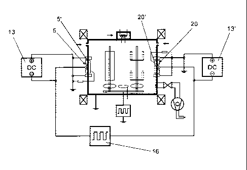
According to the invention, in addition to a first arc vaporizer source (5)
with the target
electrode (5'), a second arc vaporizer source (20) with the second target
electrode (20') is
provided, as is shown in Figure 2. Both arc vaporizer sources (5, 20) are each
operated
with one DC power supply (13) and (13') such that the DC power supplies with a
base
current ensure that the arc discharge is maintained. The DC power supplies
(13, 13')
correspond to present prior art and can be cost-effectively realized. The two
electrodes
(5', 20') which form the cathodes of the two arc vaporizer sources (5, 20) are
connected
according to the present invention with a single pulsed power supply (16),
which is
B2005389PCT W006/099760e
8
CA 02601729 2007-09-17
capable to output to the two electrodes (5', 20') high pulse currents with
defined form and
edge slope of the pulses. In the depicted configuration according to Figure 2
the anodes
(6) of the two arc vaporizer sources (5, 20) are referred to the electrical
potential of the
frame of the process installation (1).
As depicted in Figure 3, it is however also possible to operate the spark
discharges
ground-free. In this case the first DC power supply (13) is connected with its
negative
pole to the cathode (5') of the first arc vaporizer source (5) and its
positive pole with the
opposite anode of the second arc vaporizer source (20). The second arc
vaporizer source
(20) is operated analogously and the second power supply (13') is connected
with the
positive pole of the anode of the first arc vaporizer source (5).
The opposite operation of the anodes of the arc vaporizer sources leads to
better
ionization of the materials in the process. The ground-free operation, or the
floating
operation, of the arc vaporizer source (5, 20) can, however, also take place
without the
use of the opposite anode feed. It is, furthermore, possible to provide a
switch (14) in
order to be able to switch optionally between floating and grounded operation.
As
before, the two electrodes (5', 20') which form the cathodes of the two arc
vaporizer
sources (5, 20) are connected according to the present invention with a single
pulsed
power supply (16).
The supply for this "dual pulsed mode" must be able to cover a multiplicity of
impedance
ranges and, nevertheless, still be "hard" in the voltage. This means that the
supply must
supply high currents, yet must, in spite of it, be capable of being largely
operated voltage-
stably. An example of such a supply is applied parallel with the same date to
this patent
application with the No. ..
The first and preferred application field of this invention is that of
cathodic spark
vaporization with two pulsed arc vaporizer sources (5, 20) as is depicted in
Figure 2. For
these applications the impedances are at intervals of approximately 0.01 E2 to
1 SI It
should here be noted that the impedances of the sources between which "dual
pulsing"
takes place, are different. The reason may be that they are comprised of
different
materials or alloys, that the magnetic field of the sources is different or
that the material
erosion of the sources is at a different stage. The "dual pulsed mode" now
permits
B2005389PCT W006/099760e
9
CA 02601729 2007-09-17
balance via the setting of the pulse width such that both sources draw the
same current.
As a consequence, this leads to different voltages at the sources. It is
understood that the
supply with respect to the current can also be loaded asymmetrically if it
appears
desirable for the conduction of the process, which is the case for graduated
layers of
different materials. The voltage stability of a supply is increasingly more
difficult to
realize, the lower the impedance of the particular plasma. Therefore short
pulse lengths
are often of advantage. The capability of being switched over or the
controlled active
trackability of a supply to different output impedances is therefore of
special advantage if
the full range of its power is to be utilized, thus for example from range 500
V/100 A to
50 V/1000 A or as is realized in the parallel application No
The advantages of such a dual pulsed cathode configuration, in particular
comprised of
two arc vaporizer sources, are summarized as follows:
1. Increased electron emission with steep pulses results in higher current
(also
substrate current) and increased ionization of the vaporized material and of
the
reactive gas.
2. The increased electron density also contributes to a faster discharge of
the
substrate surface, in the production of insulating layers, i.e. relatively
short
charge-reversal times on the substrate (or also only pulse pauses of the bias
voltage) are sufficient in order to discharge the forming insulating layers.
3. The bipolar operation between the two cathodic arc vaporizer sources
permits a
quasi 100% pulse/pause ratio (duty cycle), while the pulsing of a source alone
always necessarily requires a pause and therefore the efficiency is not as
high.
4. The dual pulsed operation of two cathodic spark sources, which are
opposite one
another, immerses the substrate region into dense plasma and increases the
reactivity in this region, also that of the reactive gas. This is also
reflected in the
increase of the substrate current.
5. In reactive processes in oxygen atmosphere still higher electron
emission values
can be attained in pulsed operation, and it appears that a melting of the
spark
region, as is the case in classic vaporization of metallic targets, can be
largely
avoided.
A further preferred variant of the present invention comprises that as the
second electrode
B2005389PCT W006/099760e
CA 02601729 2007-09-17
is utilized, in addition to the first electrode of the arc vaporizer source
(5), the workpiece
holder (3) with the workpieces located thereon, as is depicted in Figure 4. In
this case the
single pulsed power supply (16) is connected between the first electrode (5')
of the arc
vaporizer source (5) and the second electrode implemented as workpiece holder
(3). To
be able to attain stabler discharge conditions, the DC power supply (13) of
the arc
vaporizer source (5) can additionally simultaneously also be connected with
the second
electrode, the workpiece holder. With this bias operation the ionization
conditions, in
particular in the proximity of the workpiece surface, can also be specifically
and
purposefully affected. In this variant the impedances differ significantly
from one
another. Here also a current balance can be carried out via the voltage pulse
width.
Since the electrode emission of substrate holder and substrates differs
strongly from the
electron emission of cathodic arc vaporizer, the resulting pulsed voltage does
not have a
passage through zero (substrate is always anodic). Important in this variant
is again the
application in the production of insulating layers and additionally the
capability of acting
upon the substrate with high electron currents. This operation is primarily of
interest if
the critical issue is to dissociate reactive gases in the proximity of the
substrate surface
and simultaneously to realize high substrate temperatures.
The advantages are summarized in the following:
1. High reactivity in the proximity of the substrate
2. Efficient decomposition of the reactive gas
3. Discharge of the substrates in the deposition of insulating layers
4. Realization of high substrate temperatures is possible
A further variant of the invention is shown in Figure 5, wherein the second
electrode is
here implemented as sputter target on a sputter source (18). This sputter
source (18) is
implemented as magnetron sputter source and is in conventional manner fed with
a DC
power supply (17). With this configuration the advantages of the sputter
technique can
be combined with the advantages of the arc vaporizer technique and this can be
done
even in reactive processes, in particular in the deposition of dielectric
layers or gradient-
and alloy layers.
In this case the impedances are also very different. They are between said arc
vaporizer
B2005389PCT W006/099760e
11
CA 02601729 2007-09-17
sources and those of the sputtering with a magnetron source (10 SI - 100 52).
If the
balance for identical currents is to take place, the pulse lengths must
correspondingly be
adapted again. In this operating mode it is especially important that the DC
supplies
from the pulsed supply are decoupled through a filter, which includes, for
example,
diodes. It has been found that this mode is of advantage especially for
reactive processes
for the deposition of insulating layers, since not only for the arc vaporizer
source but
especially also for the sputter source very wide process windows can be
realized. For
example, it is possible to work with constant reactive gas flow and the
difficulties
entailed in the regulation are avoided. If the two sources are disposed
opposite one
another, the process plasma extends through the substrates to the other source
and
prevents the poisoning of the sputter target over wide regions.
Additional advantages are:
1. Highly enlarged process windows for sputter operation without target
poisoning
2. Higher reactivity, especially of the sputter process through higher
electron
densities
In a further implementation of the invention the second electrode is
implemented as a
vaporization crucible (22), which is a part of a low-voltage vaporization
device, as is
depicted in Figure 6. As already explained, the low-voltage arc discharge is
operated
with a DC power supply (21), which with its positive pole is connected to the
vaporization crucible (22), which here serves as anode, and with the negative
pole to the
filament of an opposite plasma source (9), which here serves as cathode. The
low-voltage
arc discharge can in known manner be concentrated with the coils (10, 10')
onto the
crucible (22), wherein here a vaporization material melts and vaporizes. The
pulsed
power supply (16) is again interconnected between the electrode (5') of the
arc vaporizer
source (5) and the second electrode, of the vaporization crucible (22), in
order to attain
the desired high degree of ionization. This approach also helps to reduce
splatters in the
case of materials difficult to vaporize.
It is understood that the crucible of a normal electron beam vaporizer can
also be utilized
as the second electrode for the pulsed power supply.
The advantages are:
1. Dual operation increases the ionization in thermal vaporizers
B2005389PCT W006/099760e
12
CA 02601729 2007-09-17
2. Simple combination of thermal vaporization and cathodic spark
vaporization
3. More effective decomposition and excitation of the reactive gas in the
low-
voltage arc discharge
4. Utilization of high electron currents of the spark vaporization for
another thermal
vaporization
5. Very high flexibility in the conduction of the process.
In order to attain said advantageous process properties in the different
possible
implementation forms of the invention described above, the pulsed power supply
(16)
must meet different conditions. In bipolar pulse presentation the process
should be
capable of being operated at a frequency which is in the range from 10 Hz to
500 kHz.
Due to the ionization conditions, herein important is the maintainable edge
slope of the
pulses. The magnitude of the leading edges U2/(t2 - t1), U1/(t6-t5), as well
as also the
trailing edges U2/(t4 - t3) and U1/(t8 - t7) should have at least slopes of
greater than 2.0
V/ns measured over the essential portion of the edge extension. They should,
however,
be at least in the range of 0.02 V/ns to 2.0 V/ns, preferably at least in the
range of 0.1
V/ns to 1.0 V/ns and this at least in open-circuit operation, thus without
load, however,
preferably also under load. It is understood that the edge slope has an effect
during
operation, depending on the corresponding magnitude of the loading or the
connected
impedance or the corresponding settings and as such is shown in the diagram
according
to Figure 7. The pulse widths in bipolar presentation are, as shown in Figure
7, for t4 to
ti and t8 to t5 advantageously is, wherein the pauses t5 to t4 and t9 to t8
can
advantageously be substantially 0, however, under certain preconditions, can
also be 0
.is. When the pulse pauses are > 0, this operation is referred to as gapped
and through,
for example, variable time shifts of the pulse gap widths the specific
introduction of
energy into a plasma and its stabilization can be adjusted. During operation
of the pulsed
power supply between two electrodes of different impedance, as described
above, it can
under certain conditions be of advantage if the pulse durations are kept small
in order to
limit the current rise and the pulsed power supply is operated in gapped mode.
It is especially advantageous if the pulsed power supply is laid out such that
pulsed
operation up to 500 A at a voltage of 1000 V is possible, wherein the pulse-
pause ratio
B2005389PCT W006/099760e
13
CA 02601729 2007-09-17
(duty cycle) must herein be taken into consideration accordingly or must be
adapted for
the laid-out possible power of the supply. Apart from the edge slope of the
pulse voltage,
it is preferably necessary to ensure that the pulsed power supply (16) is
capable of
handling a current rise to 500 A in at least 1 ps.
In the following examples the first preferred application of the invention, as
it is
schematically shown in Figure 2, will be described. In this case the pulsed
high-power
supply (16) is operated between two cathodic spark vaporization sources (5,
20). In this
operating mode process stability for insulating layers, splatter reduction and
higher
reactivity of the plasma are achieved.
Example 1:
Description of a typical process sequence for the production of an Al-Cr-0
layer.
In the following a typical sequence of a substrate treatment in a reactive
spark coating
process is described utilizing the present invention. In addition to the
coating process
proper, in which the invention is realized, other process steps will also be
described
which relate to the preparatory and subsequent processing of the substrates.
All of these
steps allow broad variations, under certain conditions some can also be
omitted,
shortened or lengthened or be combined differently.
In a first step the substrates are customarily subjected to wet chemical
cleaning, which,
depending on the material and prior history, is carried out differently.
1. Preparatory processing (cleaning, etc.) of the substrates (methods known
to the
person skilled in the art.
2. Placing the substrates into the holders provided for this purpose and
introduction
into the coating system.
3. Pumping the coating chamber to a pressure of approximately 10-4 mbar by
means
of a pump system known to the person skilled in the art (forepumps/diffusion
pump,
forepumps/turbomulecular pump, final pressure approximately 10-7 mbar
achievable)
B2005389PCT W006/099760e
14
CA 02601729 2007-09-17
4. Starting the substrate pretreatment under vacuum with a heating step in
an argon-
hydrogen plasma or another known plasma treatment. Without limitation, this
pretreatment can be carried out with the following parameters:
Plasma of a low-voltage arc discharge with approximately 100 A discharge
current, up to
200 A, up to 400 A, the substrates are preferably connected as anode for this
low-voltage
arc discharge.
Argon flow 50 sccm
Hydrogen flow 300 sccm
Substrate temperature 500 C (partially through plasma heating, partially
through
radiation heating)
Process time 45 min
During this step a supply is preferably placed between substrates and ground
or another
reference potential, with which the substrates can be acted upon with DC
(preferably
positive) or DC pulsed (unipolar, bipolar) or as MF or RF.
5. Etching is started as the next process step. For this step the low-
voltage arc is
operated between the filament and the auxiliary anode. A DC, pulsed DC, MF or
RF
supply is connected between substrates and ground and the substrates are
preferably acted
upon with negative voltage. With the pulsed and MF, RF supplies, positive
voltage is
also applied to the substrates. The supplies can be operated unipolarly or
bipolarly. The
typical, however not exclusive, process parameters during this step are:
Argon flow 60 sccm
Discharge current low-voltage arc 150 A
Substrate temperature 500 C (partially through plasma heating, partially
through
radiation heating)
Process time 30 min
In order to ensure the stability of the low-voltage arc discharge during the
production of
insulating layers, the work is either carried out witha hot, conductive
auxiliary anode or a
pulsed high-power supply is interconnected between auxiliary anode and ground.
6. Start of coating with the intermediate layer (approximately 15 min)
CrN intermediate layer 300 nm by means of spark vaporization (source current
140 A, N2
B2005389PCT W006/099760e
CA 02601729 2007-09-17
1200 sccm, with bipolar bias of -180 V (36 gs negative, 4 gs positive).
The coating can take place with and without low-voltage arc.
Up to this point the method follows that of prior art as is reflected by
example in Figure
1.
7. Transition to the functional layer (approximately 5 min)
In the transition to the functional layer proper the nitrogen is ramped from
1200 sccm
down to approximately 400 sccm and subsequently an oxygen flow of 300 sccm is
switched on. The DC supply current for the Cr spark cathode is simultaneously
increased
to 200 A. The Al spark cathode is subsequently switched on and also operated
at a
current of 200 A. The nitrogen flow is now switched off and the oxygen flow is
subsequently run up to 400 sccm.
8. Coating with the functional layer
The bipolarly pulsed high-power supply (16), as shown in Figure 2, is now
taken into
operation between both spark cathodes. In the described process, work took
place with a
positive or negative time mean value of the current of approximately 50 A. The
pulse
durations are each 20 is for the positive as well as the negative voltage
range. The peak
value of the current through the bipolarly pulsed power supply depends on the
particular
pulse form. The difference of DC current through the particular spark cathode
and peak
value of the bipolarly pulsed current must not fall below the so-called
holding current of
the spark cathode since otherwise the spark is extinguished.
During the first 10 minutes of the coating the bias is ramped from -180 V to -
60 V. The
typical coating rates for doubly rotating substrates are between 3 gm/hr and 6
gm/hr.
The coating of the substrates with the functional layer proper thus takes
place in pure
reactive gas (in this example oxygen). The most important process parameters
are once
again summarized:
Oxygen flow 300 sccm
Substrate temperature 500 C
DC source current 200 A, for the Al as well as also for the Cr source.
B2005389PCT W006/099760e
16
CA 02601729 2007-09-17
,
The bipolarly pulsed DC current between the two cathodes has a frequency of 25
kHz.
Process pressure approximately 3 x 10⁻³ mbar
As already stated, the coating can also take place simultaneously with the
operation of the
low-voltage arc. In this case a further increase of the reactivity is
primarily achieved in
the vicinity of the substrates. The simultaneous use of the low-voltage arc
during the
coating has, in addition, also the advantage that the DC component at the
sources can be
reduced. With higher arc current, this can be further reduced.
The coating process conducted in this way is stable over several hours. The
spark target
is covered with a thin smooth oxide layer. This is desirable and also a
precondition for a
largely splatter-free and stable process. The covering becomes manifest in an
increase of
the voltage at the spark target as was also already described in the preceding
patent
application CH00518/05.
In the following, three further application examples will be cited in which,
however, only
the deposition of the interface and the functional layer will be discussed.
Example 2:
While in the above example the production of an Al-Cr-0 layer was described,
in which
only two spark targets were utilized, in the following the process for a pure
aluminum
oxide layer utilizing 4 spark targets will be described:
For the coatings, hard metal indexable inserts (tungsten carbide) were used as
substrates,
which had already been coated in a preceding process with a 1.5 lim thick TiN
layer. The
substrates were subjected to a pretreatment, which was substantially identical
to the
above described steps 1 to 5. Before the coating with the functional layer, no
special
intermediate layer was deposited, i.e. the functional layer was directly
deposited on the
TiN base and steps 6 and 7 were omitted. For the deposition of the functional
layer (8)
work took place with four spark targets and the following process parameters
were used:
= 4 Al targets operated at 170 A DC each
= bipolar current pulses, corresponding to Figure 2, of 2 Al targets each
with
B2005389PCT W006/099760e
17
CA 02601729 2007-09-17
an output voltage of 100 V at the power supply and positive and negative
pulse widths of 20 .is each
= Argon flow: 50 sccm
= Oxygen flow: 700 seem
= Substrate bias: DC bipolarly pulsed, +/- 100 V,
38 Os negative, 4 sp. positive
= Substrate temperature: 695 C
The layer obtained in this manner was characterized using the following
measurements:
= Layer thickness with double rotation of the substrates: 4 iint
= The layer adhesion was determined at HF1 to HF2 in Rockwell
indentation tests
= The microhardness was determined with the Fischerscope
(microindentation at F = 50 mN/20 s) and was HV = 1965 (+/- 200), Y =
319 GPa (+/- 12 GPa).
XRD spectra of the layer were obtained for the angular range 20/0 as well as
for grazing
incidence (3 ). These X-ray measurements show a crystalline layer with
possibly small
contributions of amorphous aluminum oxide. The aluminum oxide can clearly be
identified as (7-A1203 phase.
Example 3:
The next example relates to the production of a zirconium oxide layer. Before
the
coating with the functional layer proper, the substrates were coated with an
intermediate
layer of ZrN. For this coating 4 targets were used for the work, which was
operated at a
partial pressure of nitrogen of 2 Pa with 170 A each. The substrate
temperature was
500 C and a substrate bias of -150 V was used. The coating time for this
intermediate
layer was 6 min.
For the deposition of the functional layer (8) work also took place with four
spark targets,
corresponding to Figure 2, and the following process parameters were used:
= 4 Zr targets operated at 170 A DC each
= bipolar current pulses of 2 Zr targets each with an output voltage of 100
V
at the power supply and positive and negative pulse widths of 20ps each
B2005389PCT W006/099760e
18
CA 02601729 2007-09-17
= Argon flow: 50 seem
= Oxygen flow: 700 seem
= Substrate bias: DC bipolarly pulsed, +/- 40 V, 38 six negative, 4 si.t
positive
= Substrate temperature: 500 C
The layer obtained in this manner was characterized using the following
measurements:
= Layer thickness with double rotation of the substrates: 6.5
= The layer adhesion was determined at HF1 with Rockwell indentation
tests.
= The microhardness was determined using the
Fischerscope (microindentation at F = 50 mN/20 s) and was HV = 2450.
= The layer values for the roughness were Ra = 0.41 p.m, R= 3.22 gm, Rim),
= 4.11 m
= The coefficient of friction was determined at 0.58.
By measuring the XRD spectra of the layer, a baddeleyite structure could
uniquely and
unambiguously be determined.
Example 4:
In the last example the production and analysis of an SiAlN layer will be
discussed.
Before the coating proper with the functional layer, the substrates were
coated with an
intermediate layer of TIN. For this coating the work took place with 2
targets,
corresponding to Figure 2, which were operated at 180 A each at a partial
pressure of
nitrogen of 0.8 Pa. The substrate temperature was 500 C and a substrate bias
of -150 V
was used. The coating time for this intermediate layer was 5 min.
= 2 SiAl targets with a ratio of Si/A1 of 70/30 were operated at 170 A DC
each
= bipolar current pulses of the 2 SiAl targets with an output voltage of
100 V
at the power supply and positive and negative pulse widths of 20 us each
= Argon flow: 50 seem
= Oxygen flow: 800 seem
= Substrate bias: DC bipolarly pulsed, +/- 40 V, 38 [is negative, 41.ts
B2005389PCT W006/099760e
19
CA 02601729 2007-09-17
positive
= Substrate temperature: 410 C
The layer obtained in this manner was characterized through the following
measurements:
= Layer thickness with double rotation of the substrates: 6.5 gm
= The layer adhesion was determined at HF2 in Rockwell indentations tests.
= The microhardness was determined with the Fischerscope
(microindentation at F = 50 mN/20 s) and was HV = 1700.
= The layer values for the roughness are Ra = 0.48 gm, R, = 4.08 gm, Rmax =
5.21 gm
= The coefficient of friction was determined to be 0.82.
B2005389PCT W006/099760e