Note : Les descriptions sont présentées dans la langue officielle dans laquelle elles ont été soumises.
CA 02604661 2007-10-12
WO 2006/113537 PCT/US2006/014252
METHOD AND APPLICATIONS TO ENHANCE AND IMAGE
OPTICAL SIGNALS FROM BIOLOGICAL OBJECTS
RELATED APPLICATIONS
This application claims the benefit of U.S. Patent Application No. 60/671,397
filed
April 14, 2005 entitled "Method and Applications to Enhance and Image Optical
Signals
from Biological Objects" which is incorporated herein by reference in its
entirety.
FIELD OF DISCLOSURE
The present disclosure relates to Raman imaging using surface enhanced Raman
spectroscopy substrates.
BACKGROUND
Surface Enhanced Raman Spectroscopy ("SERS") is an interesting phenomenon,
but it is neither well understood, nor reproducible, nor controllable. Most
understanding
and SERS work is currently performed on small metal particles to enhance the
Raman
signal. Currently SERS is applied to enhance the Raman signals of relatively
small
molecules on surfaces and not large biological entities. Originally SERS was
created on
electrochemically roughened noble metal surfaces which proved hard to
characterize and
reproduce. Most of the more recent SERS work involves use of small, 20-200nm
diameter, colloidal particles of Ag or Au due to ease of fabrication and
reproducibility. In
some cases these particles are treated so that a ligand is attached which acts
to bind it to a
particular chemical entity. In cases of biological samples, such ligands are
referred to as
immuno tags which can bind to a well defined protein or receptor in the
biological sample.
Such tagging is widely used in other medical fields as well but depends on the
specific
targeted object, thereby preventing this from being a general method to study
any material
or target entity.
1
CA 02604661 2007-10-12
WO 2006/113537 PCT/US2006/014252
SERS studies have been largely limited by the small size of the SERS probe
which
has typically been comprised of nano-particles or structures that provide an
enhancement
at or nearby the structures, typically within nanometers from such structures
but as much
as five nanometers from the structures. Most SERS and the phenomenology to
understand
and direct the design of SERS substrates or targets have been based on the
desire to
maximize the resulting signal from specific molecules not the spatial
localization of the
enhancement nor the uniformity of the enhancement of the biological objects.
Most cases
of large SERS require the molecules to be directly bound to the SERS surface
thereby
allowing new electronic states and optical transitions that lead to strong
polarization of the
molecule /surface (or particle) complex. It is also known that the local
electromagnetic
fields are enhanced by small particles or by the creation of localized static
fields or
"plasmons" in free electron like metals such as Ag or Au, eitller as small
particles, or
aggregates of small particles. Designed physical Ag or Au structures such as
gratings or
arrays are known to couple the incident electromagnetic field to the object to
produce
resonant field enhancements associated with the plasmons of these structures.
These
enhanced fields give rise to enhancement of the Rainan signal that is combined
with any
shorter range chemical enhancement. In many cases of small particles, these
plasmon
fields are very confined and give rise to large SERS enhancements.
The SERS phenomena has been widely studied and has been implemented in
numerous ways, for example using Noble metals of Ag and Au in
electrochemically
roughened surfaces, colloidal particles, sol gels, grating surfaces,
microarrays of deposited
material, overcoatings on latex spheres and nanofibers, novel material nano-
fabrication
approaches, lithographically formed nano-arrays and even photonic crystal
arrays to name
2
CA 02604661 2007-10-12
WO 2006/113537 PCT/US2006/014252
a few. To date, a wide range of results are purported citing various high
levels of Raman
enliancement of 107 to 1014.
SERS studies of biological entities include the introduction of small nano-
particles
into cells that may attach to some intracellular biological materials,
attachment of
colloidal particles to biological objects in solution, disruption of the cell
to expose cellular
content to the SERS active sites of a substrate or the combined use of
antibody-active
SERS particles with both antibody and SERS ligands. Such SERS labeled immuno-
tagged particles could allow Raman scattering intensities that rival
fluorescent tags, with
the advantage that Raman would enable many more tags to be detected at one
time than
possible with fluorescent tags. The drawback of this latter approach for Raman-
tagged
assays is that immuno-labeling is a reagent based system, i.e., not general,
and dependent
on having the right immuno-tags and the right chemistry to bond both tag and
Raman
ligand on the same particle. It is also limited by the need to know the
identity of the target
material and have an appropriate immunoassay to attach to the target material
in the
,, . ,..,...
biological object.
SUMMARY
The present disclosure provides for a method for imaging biological objects. A
SERS surface is provided having a plurality of enhancing structures
distributed on the
surface wherein the surface includes a two dimensional area of at least 5 x
105 nm2. A
biological material is deposited on the SERS surface. The biological material
on the
SERS surface is illuminated, via a monochromatic light source, producing
Rainan
scattered photons. The Raman scattered photons are filtered using a two-
dimensional
tunable filter, in a plurality of predetermined wavelength bands. A two-
dimensional array
3
CA 02604661 2007-10-12
WO 2006/113537 PCT/US2006/014252
detector detects the filtered Raman scattered photons, in a spatially accurate
manner. The
results of filtering and detecting steps are combined to produce a plurality
of spatially
accurate wavelength resolved Raman images of the biological material. In one
embodiment, the enhancing structures are uniformly distributed over the
surface. In
another embodiment, the enhancing structures have a size, in at least one
dimension of
height, width and length, ranging from 100 mn to 1000 nm.
In one embodiment, the biological material on the SERS surface is illuminated
along a first optical path producing Raman scattered photons, along a second
optical path,
wherein the first optical path is at an oblique angle with respect to the
second optical path.
In another embodiment, the steps of illuminating, filtering and detecting are
repeated at a plurality of focus depths generating a plurality of outputs. The
output is
combined to construct a volumetric image of said biological material deposited
on the,
. ,~.
SERS surface.
In yet another embodiment, the SERS surface is supported on a transparent
substrate.
The present disclosure further provides for a method for imaging biological
objects. A SERS surface is provided having one of the following: a plurality
of
nanostructures uniformly distributed on the surface and a plurality of
inesostructures
uniformly distributed on the surface. A biological material is deposited on
the SERS
surface. A reagent is provided between the biological material and the SERS
surface.
The biological material on the SERS surface is illuminated, via a
monochromatic light
source, producing Raman scattered photons. The Raman scattered photons are
filtered
using a two-dimensional tunable filter, in a plurality of predetermined
wavelength bands.
4
CA 02604661 2007-10-12
WO 2006/113537 PCT/US2006/014252
A two-dimensional array detector detects the filtered Raman scattered photons,
in a
spatially accurate manner. The results of filtering and detecting steps are
combined to
produce a plurality of spatially accurate wavelength resolved Raman images of
the
biological material.
The present disclosure further provides for a method for imaging objects. A
SERS
surface is provided having a plurality of enhancing structures distributed on
the surface
wherein the surface includes a two dimensional area of at least 5 x 10⁵ nma. A
material is
deposited on the SERS surface where the material has at least one dimension of
length or
width of at least 600 nm. The material on the SERS surface is illuminated, via
a
monochromatic light source, producing Raman scattered photons. The Raman
scattered
photons are filtered using a two-dimensional tunable filter, in a plurality of
predetermined
, ~ ~. .
wavelength bands. A two-dimensional array detector detects the filtered Raman
scattered
photons, in a spatially accurate manner. The results of filtering and
detecting steps are
coinbined to produce a plurality of spatially accurate wavelength resolved
Raman images
of the material. In one einbodiment, the enhancing structures are uniformly
distributed
over the surface. In another embodiment, the enhancing structures have a size,
in at least
one dimension of height, width and length, ranging from 100 nm to 1000 nm.
The present disclosure provides for an apparatus used as a diagnostic probe
placed
on a sample such as tissue, organ or body part. The apparatus includes a
monochromatic
light source, a plurality of optical fibers, a SERS surfaces, a two
dimensional tunable
filter, a two dimensional detector and a processor. The optical fibers
transmit
substantially monochromatic light to a sample and receive Raman scatter
photons
produced by the sample. The SERS surfaces are located on the exterior of the
substrate.
5
CA 02604661 2007-10-12
WO 2006/113537 PCT/US2006/014252
The SERS surface has enhancing structures distributed on the surface which
includes a
two dimensional area of at least 5 x 10⁵ nm2 and the enhancing structures have
a size, in at
least one dimension of height, width and length, ranging from 100 nm to 1000
nm. A two
dimensional tunable filter filters the Raman scattered photons in a plurality
of
predetermined wavelength bands. A two dimensional detector detects the
filtered Rainan
scattered photons, in a spatially accurate manner, and generates outputs in
response to the
Raman scattered photons in a plurality of predetermined wavelength bands. A
processor
combines the outputs of the two dimensional detector to produce a plurality of
spatially
accurate wavelength resolved Raman images of the sample.
BRIEF DESCRIPTION OF THE DRAWINGS
The accompanying drawings, which are included to provide further
understanding of the disclosure and are incorporated in and constitute a part
of this
specification, illustrate einbodiments of the disclosure and, togetller with
the description,
serve to explain the principles of the disclosure.
In the drawings:
Figure 1 illustrates an exemplary system used in connection with the
present disclosure;
Figure 2 illustrates an exemplary system used in connection with the
present disclosure;
Figure 3 illustrates an exemplary system used in connection with the
present disclosure;
Figure 4 illustrates an exemplary SERS surface having meso-structures
uniformly distributed across the surface;
6
CA 02604661 2007-10-12
WO 2006/113537 PCT/US2006/014252
Figure 5 illustrates biological entities distributed on an exemplary SERS
surface having meso-structures uniformly distributed across the surface;
Figure 6A and 6B illustrate a simulation of Raman enhancement for short
range enhancement and long range enhancement;
Figure 7 illustrates an exemplary device of the present disclosure;
Figure 8 illustrates an exemplary system used in connection with the
present disclosure; and
Figure 9 is a flow chart illustrating an embodiment of the present
disclosure.
DESCRIPTION OF THE EMBODIMENTS
Reference will now be made in detail to the einbodiments of the present
disclosure, examples of which are illustrated in the accompanying drawings.
Wherever
possible, the same reference numbers will be used throughout the drawings to
refer to the
same or like parts.
This disclosure provides for a SERS surface having enhancing structures
distributed over the surface wherein the surface includes a two dimensional
area of at least
5 x 10⁵ nmZ. In one embodiment the enhancing structures have a size, in at
least one
dimension of height, width and length, ranging from 100 nm to 1000 nm. The
surface is
used for the deposition and detection of biological objects having enhanced
Raman
scattering. The disclosure further provides for methods to produce a plurality
of spectrally
resolved images and a plurality of spatially resolved spectra, having an
enhanced Raman
signal, of the biological material deposited on the enhancing structures SERS
surface.
The uniform SERS surface will enhance the Raman signal 100- 1000 times, in a
manner
7
CA 02604661 2007-10-12
WO 2006/113537 PCT/US2006/014252
which is uniforin over an area and extends significantly further away from the
surface so
as to obtain spatially accurate Raman images of large biological objects. The
methods of
this disclosure will permit significantly faster spatially resolved Raman
imaging from
biological objects than previously possible. The imaging will be performed
without the
need for chemical tagging of the molecular components in the biological
object.
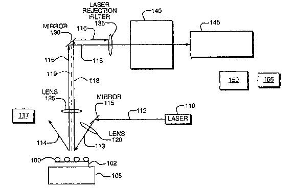
Figure 1 illustrates one embodiment of a system which may be used to carry out
the methods of the present disclosure. Sample 100 is deposited on a uniformly
structured
SERS surface 102 positioned on substrate 105. Light source 110 illuminates
sample 100
with a plurality of photons resulting in Raman photons scattered from the
sample. Light
10, source 110 can include any conventional photon source, including laser,
LED, and other
IR or near IR devices. Light source 110 may also be oriented or selected to
provide
evanescence illumination of the sample.
In one enibodiinent, the monochromatic light source 110 is positioned to
provide
incident light along a first optical path 113, which is at an angle to sample
100, as opposed
to light shining ortllogonal to sample 100, as illustrated in Figure 1. In
other words, the
radiation used to illuminate the sample need not pass through the optical
train of a
conventional microscope (or macroscope); rather, it can illuminate the sainple
at an
oblique angle from above or below sample 100. Photon beam 112 is received and
deflected by mirror 115 through lens 120. Lens 120 may optionally be used to
focus the
light on sainple 100. Alternatively, the photon beam 112 may be directed
towards the
sample 100 without the need for the mirror 115.
The multitude of photons in beam 112 reaching sample 100 illuminate the sample
and are scattered from different locations on or within the sample. Scattered
photons are
schematically represented as beams 116 and 118 while specularly reflected
photons are
8
CA 02604661 2007-10-12
WO 2006/113537 PCT/US2006/014252
represented schematically as beam 114. The scattered photons are produced
along a
second optical path 119, wherein the first optical path 113 is at an oblique
angle with
respect to the second optical path 119.
Figure 3 illustrates another embodiment of a system used to carry out the
methods
of the present disclosure. The monochromatic light source 110 is positioned to
provide
incident light along optical path 119 which is orthogonal to sample 100. The
incident
ligllt used to illuminate the sample passed througll the optical train of a
conventional
microscope. Scattered photons are schematically represented as beams 116 and
118
which are produced along optical path 119.
Referring to Figure 1, optical lens 125 is positioned along the second optical
path
119 to collect scattered photons. Optical lens 125 may be used for gathering
and focusing
received photon beams. This includes gathering and focusing both polarized and
un-
polarized photons. The focus depth may be changed by varying the location of
optical
lens 125 relative to sample 100. In general, the sample size and desired
magnification
determine the choice of light gathering optical lens 125. For example, a
microscope lens
may be employed for analysis of sub-micron to micrometer specimens. For larger
samples, macro lenses can be used. Optical lens 125 (as well as lens 120) may
include a
simple reduced resolution/aberration lens with a larger numerical aperture to
thereby
increase the system's optical throughput and efficiency. Mirror 130 is
positioned to direct
scattered photon beains 118 to tunable filter 140. It should be noted that
placement of
mirror 130 is optional and may be unnecessary in configurations where the
tunable filter is
positioned above sample 100.
9
CA 02604661 2007-10-12
WO 2006/113537 PCT/US2006/014252
Laser rejection filter 135 may be positioned prior to tunable filter 140 to
filter out
elastic scattered illumination light represented by beam 116 and to optimize
the
performance of the system. In other words, rejection filter 135 enables
spectral filtering
of the photons at the illuminating wavelength.
With further reference to Figure 1, a filter 140 passes the scattered photons
into a plurality of predetermined wavelength bands. The filter 150 may include
a tunable
filter corresponding, for example, to an electro-optical tunable filter,
liquid crystal tunable
filter ("LCTF"), an acousto-optical tunable filter ("AOTF"), a Fabry Perot
angle tuned
filter, a Lyot filter, an Evans split element liquid crystal tunable filter, a
Solc liquid crystal
tunable filter, a spectral diversity filter, a photonic crystal filter, a
fixed wavelength Fabry
Perot tunable filter, an air-tuned Fabiy Perot tunable filter, a mechanically-
tuned Fabry
Perot tunable filter, and a liquid crystal Fabry Perot tunable filter. The
filter 140 is
positioned in the second optical path 119. The plurality of predetermined
wavelength
bands include specific wavelengths or ranges of wavelengths. In one
embodiment, the
predetermined wavelength bands include wavelengths characteristic of the
sample
undergoing analysis. The wavelengths that can be passed through filter 140 may
range
from 200 nm (ultraviolet) to 2000 nin (i.e., the near infrared). The choice of
filter depends
on the desired optical region and/or the nature of the sample being analyzed.
The filer is
selected to operate in one or more of the following spectral ranges: the
ultraviolet (UV),
visible, and near infrared.
In another embodiment, the filter may include a two dimensional grating
disperser which includes a hologram grating. The hologram grating is
fabricated using E-
beam fabricated lithography. Grating may be fabricated to achieve spectral
wavelength
CA 02604661 2007-10-12
WO 2006/113537 PCT/US2006/014252
resolution in the visible, UV, infrared or near-infrared wavelength range. The
grating is
fabricated to achieve spectral resolution over a Raman Shift value in a
spectra range of
2800 cm 1 to 3200 cm 1 corresponding to the carbon-hydrogen stretching modes.
In a
second embodiment, the grating 108 is fabricated to achieve spectral
resolution over a
Raman Shift value in the fingerprint region corresponding to a spectra range
of 500 cm I
to 2000 cm'. Computed Tomography Imaging Spectroscopy ("CTIS") used as a
spectral
imaging tool is described in U.S. Patent Appl. No. 11/336,588 entitled "Method
for
Raman Computer Tomography Imaging Spectroscopy," which is incorporated herein
by
reference in its entirety.
A first two-dimensional array of detection elements 145 ("first detector")
detects filtered Raman scattered photons in a spatially accurate manner to
generate output
to processor 150. The first detector may include a digital device such as an
image focal
plane array ("FPA") CCD or CMOS sensor. The optical region employed to
characterize
the sample of interest governs the choice of the first two-dimensional array
detector. For
exainple, a two-dimensional array of silicon charge-coupled device ("CCD")
detection
elements can be employed for image analysis with visible wavelength
fluorescence and
Rainan spectroscopy, while galliuin arsenide (GaAs) and gallium indium
arsenide
(GaInAs) FPA detectors can be employed for image analyses at near infrared
wavelengths. The choice of such devices depends on the type of sample being
analyzed.
The first detector 145 detects, in a spatially accurate mamier, the scattered
photons passed
by the tunable filter 140. In one embodiment, each detection element in the
first two-
dimensional array of detection elements used to form the detection array 145
functions to
detect photons scattered from a different spatial location on or within the
sample. In one
embodiment, the first two-dimensional array of detection elements 145 produces
digital
11
CA 02604661 2007-10-12
WO 2006/113537 PCT/US2006/014252
images of the entire view of the sample as processed by tunable filter 140.
A second two-dimensional array of detection elements 117 ("second
detector") may include a digital device such as for example CCD or CMOS sensor
to
detect reflected photons.
Fig. 2 schematically represents a system according to yet another
embodiment of the disclosure. More specifically, Fig. 2 schematically shows a
high
optical throughput configuration for imaging using low light levels at
variable
magnification. The collection of optics is similar to that illustrated in Fig.
1, but with
illumination from the underside of sainple 100.
It is noted that in both Figs. 1 and 2, sample 100 is illuminated at an
oblique angle. Specifically referring to Fig. 2, photon beam 113 and the plane
axis of
sample 100 define an oblique angle. It has been found that through oblique
illumination, a
so-called "Dark Field Raman Imaging" is developed. As opposed to the
conventional
,,..~
bright field Raman configuration, the dark field Raman imaging decouples the
image
capture optics from the delivery of exciting radiation. Consequently, internal
scattering
and attenuation of the incident radiation has been minimized to improve the
signal to
noise ratio. Also, the location of the optical source external to the optical
train further
allows the use of a lower cost, less powerful illumination source as well as
enables a
simpler, less expensive integration of several illumination sources into the
system. In
addition, it allows for coupling of the illumination beam into devices such as
waveguides,
integrated optics and microfluidic devices.
In each of the embodiments shown in Figs. 1, 2, and 3 at least one processor
150 is
coupled to and used to control the optical devices of the apparatus
illustrated in Figs. 1
12
CA 02604661 2007-10-12
WO 2006/113537 PCT/US2006/014252
and 2, including lenses 120, 125, 135, mirrors 115, 130, tunable filter 140,
first detector
145 and second detector 117. Processor 150 combines the results from the
tunable filter
140 and the first detector 145 to generate a plurality of spatially resolved
Raman spectra
and/or a plurality of spectrally resolved Raman images. The resultant
spatially accurate
wavelength resolved Raman images are then processed using reference databases
155 or
statistical techniques applicable to spectroscopic data to generate an image
of relevant
biological information about the sample.
The output generated by exemplary systems illustrated in Figures, 1, 2 and
3, includes a three dimensional block of data or a hypercube with spatial
dimensions in the
x and y dimensions and wavelength or frequency in the z dimension. From the
hypercube,
a plurality of spectra for each pixel of the image plane may be selected for
analysis or a
plurality of spatially accurate wavelength resolved images may be selected for
analysis.
The data contained witllin the hypercube may be analyzed by multivariate
(chemometric)
analysis techniques such as principal component analysis, principal component
regression
and partial least squares modeling to generate a chemical image. The
information within
the chemical image includes, spatial, chemical, structural, and functional
information
characterizing the material under analysis.
With reference to Figure 4, a schematic diagram illustrates a SERS surface
having
enhancing structures 410 distributed across the surface where the surface
includes a two
dimensional area of at least 5 x 10⁵ nm2. In one embodiment, the enhancing
structures are
uniformly distributed across the surface. In another embodiment, the enhancing
structures
will have a size of 100-1000 nm size, in at least one dimension of height or
width or
length, which are uniformly distributed over the surface. An enhancing
structured SERS
13
CA 02604661 2007-10-12
WO 2006/113537 PCT/US2006/014252
surface is shown in contrast to a nano-structured surface 420 having structure
on a
significantly smaller scale, of 0.1 to 10 nm. The enhancing structure SERS
surface will
exhibit electromagnetic enhancement and/or chemical enhancement of the Raman
signal.
It is envisioned that the enhancing structure SERS surface will have extended
Plasmon
fields to sample the intra cellular material of biological entities at micron
distances from
the surface. Excitation of these extended plasmons can be achieved by tuning
the incident
angle to optically couple to longer period optical or meso structures on the
surface. The
enhancing structures may be fabricated by electrochemical or vapor deposition,
vapor
alloy deposition or sputtering, chemical (reactive) deposition, chemical or
electrochemical
etching, electrochemical roughening of metal surfaces, electron-beam
lithography,
semiconductor lithographic fabrication methods, colloidal preparative methods
and/or
various coinbinations of these processes. In one einbodiment, the enhancing
structure is
fabricated by etching metals from metal alloy films. In another embodiment,
the
enhancing structure is fabricated by electrochemically roughening a porous
metal film. In
another embodiment, the enhancing structure SERS surface includes a gold
surface. In yet
another embodiment, the enhancing structure SERS surface includes a silver
surface.
Methods for making enhancing structure SERS surfaces is described in U.S.
Patent
Publication No. 2006/0061762 which is incorporated herein by reference in its
entirety.
In one embodiment, the SERS surface having a plurality of enhancing structures
distributed on the surface is envisioned as a porous film showing point to
point variations
in signal enhancement having standard deviations of only :L 15%. This is in
contrast to
prior art SERS substrates having point to point variations of 200% to
200,000%. In
another embodiment, the enhancing structure SERS surface is envisioned as a
textured
metal film with areas of pores and metal film.
14
CA 02604661 2007-10-12
WO 2006/113537 PCT/US2006/014252
Referring to Figure 5, a schematic diagram illustrates exemplary biological
materials 520, 530 distributed on an exemplary SERS surface having enhancing
structures
510 distributed across the surface 505. Representative biological entities,
sizes and shape
include: staphylococcus - 700 nm diameter sphere; E-coli bacteria - 600x2000
nm shaped
rod; anthrax cyst - 1000-2000 nm shaped oblong; blood cell - 2000x8000 nm
shaped
saucer; epithelial cells - 10000 x 50000nm shaped flat blob. In one
embodiment, it is
envisioned that the structures will be uniformly distributed in the x- and y-
directions of
the SERS surface so that the surface of a biological material will have
substantially
homogeneous contact with the SERS enhancing structures without areas deficient
of
surface structures. The unifonn enhancing structures SERS surface will provide
substantially uniform Raman signal enhancement across its surface. For
example, a
uniform structure SERS surface having enhancing structures extending over 1000
nm in
,
diameter may be used to enhance the Raman scattering signal of a
staphylococcus
bacterium. For example, a uniform structure SERS surface having enhancing
structures
extending over 3000 nm in the x-direction and 1000 nm in the y-direction may
be used to
enhance the Ranlan scattering signal of an anthrax spore. As shown in Figure
5, the
electromagnetic enhancement and/or chemical enhancement of larger biological
entities
will require different electromagnetic field patterns than those for small
molecule bound
to the surface. The localized electromagnetic field of a compact uniform
structure SERS
,,,
surface' will likely have sufficient electromagnetic enhancements to probe
inside the
outermost layers of biological objects. To spatially probe deeper, requires
the more
extended electromagnetic fields of uniform denriditic-like structure features
410 shown in
Fig 4. In changing the incidence angle, the ratio of the long range and short
range
CA 02604661 2007-10-12
WO 2006/113537 PCT/US2006/014252
enhancements will change and allow one to discriminate between these two
components
of the SERS enhancement.
In one embodiment, the material includes tissue samples such as thin sections
of
fresh or paraffin embedded tissue. In another embodiment, the sample includes
cellular
samples such as those routinely obtained in Fine Needle Aspiration, urine
cytology,
bronchial lavage, peritoneal lavage, and cervical scraping. In another
embodiment, the
material has at least one dimension of length or width of at least 600 nm.
Figures 6A and 6B illustrates a phenomenological siinulation of the Raman
enhancement for a local short-rangp, nanostructure, chemical enhancement and
much
weaker longer-range field enhancements of a SERS surface. As shown in Figure
6A, the
highest short-range enhancement depends on strong local fields of a small
particle, or as
depicted here, a chemical effect that depends on the overlap of the wave
functions of the
metal site and molecule and their local electronic configuration. Associated
with such
wave function overlap, these enhancements die out at a distance of 5 nm from
the SERS
surface. With reference to Figure 6B, longer enhancement depends on the
electrodynamics of the surface structure and its shielding or lack thereof by
the underlying
metal or interactions with other dielectric layers. The enhancing structures
of Figure 6B
have a size ranging from 100 nm to 1000 nm, in at least one dimension of
height or width
or length. The' spatial features, such as size and shape, of the metallic
particle/feature
determine the length and screening of the longer range extended field. Figure
6B shows
two screening models for the longer-range field enhancement, where the
electron densities
fiom highly localized fields are scaled to reflect a different screening by
the substrate.
This simulation uses a screened plasmon model of the electromagnetic fields.
The spatial
16
CA 02604661 2007-10-12
WO 2006/113537 PCT/US2006/014252
extension of surface plasmons arising from silver grating structures are well
know and
have been previously observed to contribute to the total SERS enhancements
In one embodiment, the present disclosure provides for methods to image
biological materials positioned laterally across the enhancing structure SERS
surface so as
to pinpoint the locations of organelles and more accurately detect different
biochemicals
within the biological material. The higher signal to noise ("S/N") achieved
will enable the
detection of more subtle changes in these cellular chemicals that reflect
biochemical
problems, e.g., cancer or metabolic disorders. In one embodiment, the Raman
signals of
different biological materials are enhanced without the need for any special
immuno
tagging agents.
In another embodiment, volumetric imaging with an enhancing structure SERS
surface will similarly enable the real space coordinates of these biological
maerials and
their molecular identity in cells or otlier biological materials. The
volumetric image is
obtained by collecting a plurality of spatially resolved Raman spectra and/or
a plurality of
spectrally resolved Raman images at a plurality of focus deptlls. The output
generated at
the plurality of focus depths is then combined to construct a volumetric image
of the
biological entity. While the natural localization of certain chemicals within
the organelles
of cells is well known, it is necessary to have the sensitivity and resolution
to detect the
chemicais. Otherwise harvesting of such material from many cells may be
necessary to
obtain sufficient material for such an analysis which is problematical if one
has only a few
cancer cells to work with. Characterization of the distance dependence of the
enhancing
structures SERS surface will allow recalibration of the actual signal levels,
which spatially
17
CA 02604661 2007-10-12
WO 2006/113537 PCT/US2006/014252
vary in the z-direction, and reflect the actual relative concentrations of
these chemicals
throughout the cell.
In yet another embodiment, the present disclosure provides for a surface which
is
envisioned to have a reservoir of reagent at the SERS surface biological
entity interface.
This surface will permit a wide range of cell membrane and cellular metabolic
studies,
including processes and the chemistry of cell membranes. To date this
interface and its
properties have been very difficult to study due to the extremely thin bilipid
layer
(-60nm) that comprises this membrane as well as the small amount of cellular
biochemicals present there. It is furtlzer envisioned, that SERS surface
structures having
both meso-structures, 100 nm to 1000 nm in size in at least one dimension, and
nano-
structures, 1 nm to 10 nm in size in at least one dimension, for local and
extended
enhancement can allow the sampling of either or both.
In another embodiment, the present disclosure envisions the discrimination of
both
local and more distant biological entities using an enhancing structures SERS
surface. By
varying and selecting the angle of the incident light one can tune the
resulting field to
. ,,
probe locally bound structures on the membrane of the biological object or
further away
from it. This difference in sampling distance essentially exploits the long
and short range
enhancements that can arise due to different plasmons that can be excited at
off normal
incidence. Further angular modulation of the incident light can allow
comparisons of the
two regions and the direct comparison of these different signal contributions
thereby
allowing each of them to be more clearly delineated. This signal modulation
approach is
widely known and practices to separate signals, and known as differentiated
modulation or
"lock-in detection."
18
CA 02604661 2007-10-12
WO 2006/113537 PCT/US2006/014252
In another embodiment, the present disclosure envisions the fabrication of a
device
having an enhancing structures SERS surface on a transparent substrate. With
reference
to Figure 7, device 710 includes a monochromatic light source 712, a plurality
of optical
fibers 714, a SERS surface 715, the enhanced extended field 716, a transparent
substrate
717, a two dimensional tunable filter 718, a two dimensional detector 720 and
a processor
722. The optical fibers 714 transmit substantially monochromatic light to a
sample and
receive Raman scatter photons produced by the sample. The SERS surfaces 716
have
structures distributed on the exterior of the substrate surface 717 wherein
the surface
includes a two dimensional area of at least 5 x 10⁵ nm2. In one embodiment,
the structures
aarQ uniformly distributed across the surface. In another embodiment, the
enhancing
structures have a size ranging from 100 nm to 1000 nm, in at least one
dimension of
height or width or length. Two dimensional tunable filter 718 filters the
Raman scattered
photons in a plurality of predetermined wavelength bands. Two dimensional
detector 720
detects the filtered Raman scattered photons, in a spatially accurate manner,
and generates
outputs in response to the Raman scattered photons in a plurality of
predetermined
wavelength bands. Processor 722 combines the outputs of the two dimensional
detector to
produce a plurality of spatially accurate wavelength resolved Raman images of
the
sample. Device 710 allows a projection mode of illuinination and Raman
collection in a
backscattering geometry permitting illumination and detection of a solid
object upon
which the probe is placed. As illustrated in Figure 7, the plurality of
optical fibers 714
transmit and collect the illuminating and Raman scattered ligllt. In one
embodiment, the
device could be used as contact probe to be positioned or pressed into a body
part of tissue
during surgery to determine specific molecular characteristics. In another
embodiment,
the device could be used as a portable sensor probe to detect toxic powders or
liquids.
19
CA 02604661 2007-10-12
WO 2006/113537 PCT/US2006/014252
In yet another embodiment, a device is envisioned having a SERS surface on a
soft
pliable substrate which would allow a disposable sampling head used for handle
held units
.or in. particular for disposable probes that could be discarded after use by
a patient. The
use of this device would allow both a signal enhancement as well as a
discardable surface
for one time use on patients. For such patient applications it would further
be desirable to
have an optically transparent protective layer over the outer SERS surface
which may
come into contact with the patent's biological material. The protective cover
would
protect the SERS surface from degradation arising in the environment. The
protective
layer should ideally be thin to minimize separation of the material of
interest from the
SERS roughness features. Also, the protective layer should have a simple Raman
spectrum to avoid confounding the Raman signal from the material of interest.
In another embodiment, it is envisioned that the enhancing structures SERS
surface may be used for measurement of Raman optical activity and of weaker
Raman
features associated with protein chirality. Raman chirality, while having an
extremely
weak signal, can provide unique and novel information about protein folding.
Speeding
such measurements up by a thousand fold would enable a measurement that took a
week
to take 10 minutes. Alternately the ability to produce Raman enhancements over
an area
could enable measurement of spatially resolved Raman optical activity. This
could enable
pinpointing locations in a cell where unusual Raman optical activity arises.
In addition
erroneous protein folding in not only cells but in specific organelles will
also be more
efficiently'detected using such surfaces that allow sub cellular level
molecular resolution.
These protein-folding problems form the basis of several diseases, such as
Alzheimer's
and mad cow disease. Due to the need to maintain circular polarization for
Raman optical
activity, periodic structures will likely inhibit the Raman signal. It is
envisioned that
CA 02604661 2007-10-12
WO 2006/113537 PCT/US2006/014252
random structures will not interfere or significantly reduce measurement of
circularly
polarized Raman from such surfaces.
In yet another embodiment, reduced laser power, data acquisition time, and/or
improved sensitivity is envisioned for Raman spectroscopy based studies of bio-
materials
due to the enhanced signal levels possible with an enhancing structure SERS
surface of
the disclosure. In yet another embodiment, reduced laser power or data
acquisition time is
envisioned for a variety of optical spectroscopy based studies of bio-
materials.
With reference to Figure 8, an embodiment of the present disclosure
illustrates a variable angle system for imaging a sample 820 deposited on an
enhancing
structures SERS surface 810. The sample and the SERS surface are supported on
a
substrate which is located along a plane 805. The sample 820 is illuininated
with a
monochromatic light source along an optical path 840. The optical path 840 is
at an angle
of illumination 845 other than 90 with respect to the substrate plane 805.
The angle of
illumination 845 may be varied from about 0 with respect to the substrate
plane 805 to
89 with respect to the substrate plane.
In one embodiment, the present disclosure uses the system illustrated in
Figure 8 for measuring spatial and spectral infomlation from a sample
deposited on a
meso-structured SERS surface at varying angles of illumination. With reference
to Figure
9, a flow chart is shown illustrating a method of the present disclosure. In
step 910, the
sample is illuminated, with monochromatic light, along an optical path
producing Rainan
scattered photons, wherein the optical path is at a first angle of
illumination, wherein the
first angle of illumination is other than 90 with respect to the substrate
plane. In step
920, the Raman scattered photons are filtered into a plurality of
predetermined wavelength
21
CA 02604661 2007-10-12
WO 2006/113537 PCT/US2006/014252
bands. In step 930, the filtered Raman scattered photons are detected in a
spatially
acctirate manner. In step 940, a first plurality of spatially accurate,
wavelength resolved
images of the sample is generated. In step 950, the sample is illuminated,
with
monochromatic light, along an optical path producing Raman scattered photons,
wherein
the optical path is at a second angle of illumination, wherein the second
angle of
illumination is other than 90 with respect to the substrate plane. Steps 920,
930 and 940
are then repeated to generate a second plurality of spatially accurate,
wavelength resolved
images. In step 960, the first plurality of spatially accurate, wavelength
resolved images
are conipared to the second plurality of spatially accurate, wavelength
resolved Raman
images.
The present disclosure may be embodied in other specific forms without
departing
from the spirit or essential attributes of the disclosure. Accordingly,
reference should be
made to the appended claims, rather than the foregoing specification, as
indicated in the
~, .
scope of the disclosure. Although the foregoing description is directed to the
preferred
elnbodiments of the disclosure, it is noted that other variations and
modification will be
apparent to those skilled in the art, and may be made without departing from
the spirit or
scope of the disclosure.
22