Note : Les descriptions sont présentées dans la langue officielle dans laquelle elles ont été soumises.
CA 02605172 2007-10-16
1
Self-excited step-up converter
Technical field
The invention relates to an electronic ballast with a step-up
converter for operating a discharge lamp, for example a low-
pressure discharge lamp.
Prior art
Electronic ballasts for operating discharge lamps are known in
various embodiments. In general, they contain a rectifier
circuit for rectifying an AC voltage supply and charging a
capacitor, which is often referred to as an intermediate
circuit capacitor. The DC voltage present at this capacitor is
used for supplying an inverter, which drives the discharge
lamp. In principle, an inverter produces a supply voltage for
the discharge lamp to be operated with high-frequency current
from a rectified AC voltage supply or a DC voltage supply.
Similar apparatuses are also known for other lamp types, for
example in the form of electronic transformers for halogen
lamps.
Step-up converter circuits for system current harmonic
reduction of discharge lamps are known per se. They have a
storage inductor, a switching element, a diode and an
intermediate circuit capacitor. The intermediate circuit
capacitor supplies, for example, a discharge lamp via an
inverter circuit.
Description of the invention
The invention is based on the technical problem of specifying
an improved electronic ballast with a step-up converter.
The invention relates to an electronic ballast for a lamp with
a step-up converter, which has a storage inductor, a diode, an
CA 02605172 2007-10-16
2
intermediate circuit capacitor and a switching element,
characterized in that it is designed
= to switch off the switching element in the step-up
converter when a maximum current value of the current
flowing through the switching element is reached, and
= to switch on the switching element by means of a jump in
the potential between the storage inductor and the diode
after demagnetization of the storage inductor,
so that the step-up converter oscillates in self-excited
fashion.
Preferred configurations of the invention are specified in the
dependent claims and will be explained in more detail below.
The disclosure in this case always relates both to the method
category and the apparatus category of the invention.
The switch-on and switch-off times of the switching element are
very significant for the function of a step-up converter. The
invention is based on the knowledge that the value of the
current through the storage inductor may be suitable as an
indicator for the switch-on and switch-off times of the
switching element for operation.
In the switched-on state, the switching element ensures an
increasing current flow in the storage inductor up to a maximum
value which can be set. In this case, the storage inductor is
magnetized. The electronic ballast according to the invention
is designed such that the current through the storage inductor,
when the switching element is switched on, is detected for
example by means of a measuring (shunt) resistor and, when this
maximum value is reached, the switching element is switched
off. Once the switching element has been switched off, the
diode conducts the current impressed in the storage inductor
into the intermediate circuit capacitor. This current decreases
over time. If the storage inductor has been completely
demagnetized, there is no longer any current flowing through it
CA 02605172 2007-10-16
3
and the diode, which is connected in series, is off. The
potential between the storage inductor and the diode jumps from
the supply potential of the intermediate circuit capacitor to a
potential with a considerably smaller absolute value, which
corresponds to the instantaneous potential of the rectified AC
voltage supply. This potential jump can be used as an indicator
of a switch-on time of the switching element. The invention is
designed such that the switching element is now switched on.
Current is again flowing through the switching element and the
storage inductor. In this case, the storage inductor is
remagnetized.
The described sequence of such a switch-on and switch-off cycle
can repeat itself without any forced control of the switching
element. This can be referred to as "self-excited" oscillation.
The ballast according to the invention is therefore
particularly simple in terms of control and circuitry.
Furthermore, it is also particularly robust with respect to
tolerances of the storage inductor inductance.
Preferably, the jump in the potential between the storage
inductor and the diode after the demagnetization of the storage
inductor is detected by at least one output capacitor. This
potential jump can be used as an indicator of the switch-on
time of the switching element. A resistor can be connected in
series with said output capacitor.
The time constant from this resistor and the output capacitor
is so great that complete charging or discharging of the output
capacitor does not occur during the demagnetization of the
storage inductor.
In an alternative embodiment, the demagnetization is detected
by a coil which is secondary to the storage inductor.
The measuring resistor, which is preferably used for measuring
the current for determining the switch-off time of the
CA 02605172 2007-10-16
4
switching element, can be connected in series with the
switching element, advantageously in the connection between the
switching element and the reference potential.
Preferably, an embodiment of the invention has a first signal
line, which connects the control input of the switching element
to a control circuit of the step-up converter. In this case,
the signal line can be connected directly to the control input
of the switching element, or else indirectly via a circuit,
which switches the switching element, or one or more resistors.
The step-up converter can therefore be blocked by means of the
signal line by the control circuit.
A preferred embodiment of the invention has a resistor between
the supply potential of the intermediate circuit capacitor and
the control input of the switching element. If a sufficient
voltage is present at the intermediate circuit capacitor, the
switching element can be switched on via this resistor. That is
to say that the oscillation can be stimulated automatically as
no special control signals are required.
A preferred embodiment of the invention has a threshold value
element for driving the switching element. The control input of
this threshold value element is preferably connected to the
potential between the storage inductor and the diode via the
output capacitor and at least one resistor. Over this path, the
jump in the potential between the storage inductor and the
diode after the demagnetization of the storage inductor can be
used as an input signal for the threshold value element.
Furthermore, the control input of the threshold value element
is connected to the potential between the switching element and
the measuring resistor via at least one resistor. Over this
path, the threshold value element can be controlled as a
function of the current through the switching element. In order
that the control input of the switching value element is at a
defined potential at the time at which the switching element is
switched on, it can be connected to the reference potential via
CA 02605172 2007-10-16
a series circuit comprising a resistor and a diode. The node
between this resistor and the diode is in this case connected
to the series circuit comprising the output capacitor and at
least one resistor. It is thus possible to ensure that the rise
in the voltage across the measuring resistor determines the
temporal dependence of the drive potential of the threshold
value element while the switching element is switched on.
With such circuitry for the components, a cycle of the step-up
converter is as follows: in a first time section, the switching
element is switched on. The current through the switching
element is measured via the measuring resistor, which is
connected in series with the switching element. In this first
time section, this current also corresponds to the current
through the storage inductor. The potential which is tapped off
at the measuring resistor is supplied to a control input of the
threshold value element, possibly via one or more resistors, as
an input signal. If the value of the current exceeds a
predetermined maximum, the threshold value element is switched.
The required connection to the reference potential can be
produced via the series circuit (proposed in the preceding
paragraph) comprising a diode and a resistor. The maximum
CA 02605172 2007-10-16
6
depends on the selected dimensions for the components of the
circuit and in this regard is predeterminable. In particular,
these component parts may be: the measuring resistor, a
resistor via which the voltage across the measuring resistor is
tapped off and supplied to the control input of the threshold
value element, and the resistor which produces the connection
to the reference potential in series with the diode. The output
of the threshold value element is connected to the control
input of the switching element and switches it off. The
potential between the storage inductor and the diode jumps to
approximately the supply potential of the intermediate circuit
capacitor when the switching element is switched off. This
marks the end of the first time section.
In a following, second time section, the threshold value
element remains in its state owing to the output capacitor
because the potential between the storage inductor and the
diode only jumps back again when the storage inductor is
demagnetized and the threshold value element is kept in its
state via the output capacitor. The switching element in this
case remains switched off. This state is held as long as the
storage inductor demagnetizes. If the switching element were
not to be switched off permanently by the threshold value
element, the switching element could be switched on again
prematurely via the voltage at the intermediate circuit
capacitor as soon as the storage inductor has demagnetized. The
potential between the storage inductor and the diode jumps from
the supply potential of the intermediate circuit capacitor to a
potential with a much smaller value, which corresponds to the
instantaneous potential of the rectified AC voltage supply. The
threshold value element is switched via the output capacitor.
The switching element is switched on and a new cycle begins.
It can be gleaned from the above description that the clock of
the step-up converter is determined by the duration of the
demagnetization of the storage inductor. No further timing
elements are required.
CA 02605172 2007-10-16
7
Since when a supply voltage is first applied the output
capacitor and the intermediate circuit capacitor are charged
directly by the supply voltage, the drive potential of the
threshold value element cannot pass the switching threshold in
a time which is considerably longer than the period duration of
the switch-on/switch-off cycles of the step-up converter
during operation. The threshold value element cannot easily be
switched until the intermediate circuit capacitor has been
charged to the instantaneous value of the supply voltage which
is highest in terms of absolute value. During this time, the
step-up converter is blocked.
Preferably, an embodiment of the invention with a threshold
value element therefore has a second signal line, which is
connected to the control input of the threshold value element
and to the control circuit. In this case, this second signal
line can be connected to the control input of the threshold
value element via the resistor from the series circuit
comprising the diode and the resistor, which series circuit
connects the control input of the threshold value element to
the reference potential. The threshold value element can be
switched by the control circuit via the second signal line. The
step-up converter is therefore no longer blocked during first
charging of the intermediate circuit capacitor.
The use of transistors as a simple embodiment of a threshold
value element may have the disadvantage that the maximum
current through the storage inductor depends on the tolerance
of the switching threshold of the transistor, which tolerance
is not negligible. The transistor can in this case also have a
driver function for the switching element.
In a further preferred embodiment of the invention, a
comparator is therefore used as the threshold value element and
preferably a driver circuit is connected downstream of said
comparator. Thus, the dependence of the switch-on current
CA 02605172 2007-10-16
8
threshold of the threshold value element on component
tolerances and temperature dependencies can be reduced. A
driver circuit generally comprises a plurality of component
parts and may also have, inter alia, one or more transistors.
As has already been described once further above, the control
input of the threshold value element can be connected to the
reference potential via a resistor and a diode, the resistor
being connected to the control input of the threshold value
element. The series circuit comprising the output capacitor and
the resistor can be joined at the node between this resistor
and the diode. Preferably, in an embodiment of the invention, a
capacitor is connected in parallel with the resistor at the
control input. The capacitor acts as a differentiating element,
so that the jump in the potential after the demagnetization of
the storage inductor is transferred differentially to the input
of the comparator, which may accelerate the driving.
A reference signal is present at an input of the comparator,
and the signals of interest are present at the other input,
which signals are produced by the measuring resistor and the
output capacitor. Preferably, a DC voltage is superimposed on
this signal input, which DC voltage raises the potential of
this input further away from the reference potential. For this
purpose, the input node of the comparator can be connected to
the supply potential of the comparator, for example via a
resistor.
In a preferred embodiment of the invention, the reference
signal is proportional to the instantaneous value of the supply
voltage. The current drawn by the step-up converter can
therefore be approximately sinusoidal.
It is often desirable to operate step-up converters selectively
directly on the system supply or using a phase gating dimmer.
In this case, the step-up converter may need to match its
operation to a supply with or without a phase gating dimmer.
CA 02605172 2007-10-16
9
This may be the case, for example, if the operation of the
step-up converter in one of the two cases does not conform to
standards with respect to system current harmonics or the step-
up converter in one of the two cases is not functioning
effectively without its operation being changed over. It is
then necessary for it to be possible for the electronic ballast
to identify whether it is being operated directly on the system
supply or using a phase gating dimmer; it is then possible for
corresponding operational parameters to be set, for example the
switch-off current threshold.
Operation using a phase gating dimmer changes the supply
voltage present at the electronic ballast in a characteristic
fashion. This is utilized by the invention. Phase gating
dimmers only make the system supply available to the ballast
after a time, which can be set, within each system half-cycle.
During the phase gating, no input voltage is present at the
ballast. After this time, approximately the original supply
voltage is present. The voltage at the input of the electronic
ballast has a steep edge after the phase gating; jumps in the
supply voltage occur.
An embodiment of the invention has a differentiator, which is
connected between a system line and the reference potential of
the ballast. This differentiator outputs the voltage jumps in
the supply voltage. At its output, relatively large peak
voltages in terms of absolute value occur in the case of a
voltage jump. These peak voltages, after any further
processing, for example in the form of peak value
identification, can be supplied to a control circuit of the
step-up converter, which can then correspondingly set the
operational parameters of the step-up converter.
Particular problems result in the case of selective operation
of step-up converters using a phase gating dimmer or directly
on the system supply. If, for example, the step-up converter is
designed exclusively for operation using a phase gating dimmer,
CA 02605172 2007-10-16
as in EP 1 465 330 A2, in this case the following problem may
occur in the event of the lack of a phase gating dimmer: from a
certain time within a system half-cycle of the supply system at
which time the intermediate circuit capacitor has been
sufficiently charged, the current supply of the discharge lamp
is generally interrupted during the remaining time of this
half-cycle. Since there is no phase gating in the case of
direct operation on the supply system, it is possible that the
step-up converter draws no further current even relatively
early on within a system half-cycle. The power factor as a
quotient of the active power and the apparent power is low.
Furthermore, it is necessary in accordance with the standard
IEC 61000-3-2 to ensure a current consumption beyond a phase
angle of 90 .
Preferably, the electronic ballast detects, by means of the
differentiator, whether a phase gating dimmer is connected
upstream. If the ballast is functioning directly on the system
supply, the operational parameters of the step-up converter are
set in such a way that it can function so as to conform to
standards. This can take place by means of a reduction in the
switch-off current threshold of the step-up converter. The
step-up converter then draws a current having a lower
amplitude. In order to charge the intermediate circuit
capacitor to its maximum value, current is now drawn by the
step-up converter over a longer period of time within a system
half-cycle. The switch-off current threshold, in order to
comply with the standard, can be set in such a way that the
current consumption of the step-up converter extends as far as
beyond a phase angle of 90 .
The longer the time interval of the current consumption within
a system half-cycle is, the greater the power factor of the
ballast also is. Preferably, the operational parameters - in
particular the switch-off current threshold - of the step-up
converter are set in such a way that the current is drawn in
CA 02605172 2007-10-16
11
the absence of a phase gating dimmer at least over half the
duration of a system half-cycle.
In a particularly simple and therefore preferred embodiment of
the invention, the differentiator has a series circuit
comprising a capacitor and a resistor. This series circuit can
be connected to one of the system lines in series with the
reference potential of the electronic ballast. A further
capacitor can be connected to the other system line by the node
between the resistor and the capacitor. Given suitable
dimensions for the capacitance and the resistance, a voltage
which is proportional to the differentiated supply voltage is
present at the resistor. One advantage of this simple
implementation is the low number of component parts required.
Preferably, a peak value detection circuit is connected in
parallel with the resistor from the differentiator circuit
described in the previous paragraph. If the step-up converter
is operated using a phase gating dimmer, the controller of the
step-up converter can be driven by the peak value detected via
the resistor, for example by means of a switching element which
is connected to the peak value detection.
Brief description of the drawings
The invention will be explained in more detail below with
reference to exemplary embodiments. The individual features
disclosed in the process can also be essential to the invention
in other combinations. The description above and below relates
to the apparatus category and the method category of the
invention, without this explicitly being mentioned in detail.
Figure 1 shows a step-up converter circuit. This is to
be regarded as being part of an electronic
ballast according to the invention.
CA 02605172 2007-10-16
12
Figures 2a, b, c show relevant current and voltage profiles of
the circuit arrangement shown in figure 1.
Figure 3 shows a modification of the circuit
arrangement shown in figure 1.
Figures 4a, b, c show relevant current and voltage profiles of
the circuit arrangement shown in figure 3.
Figure 5 shows a circuit arrangement for detecting
phase gating in the supply voltage.
Preferred embodiment of the invention
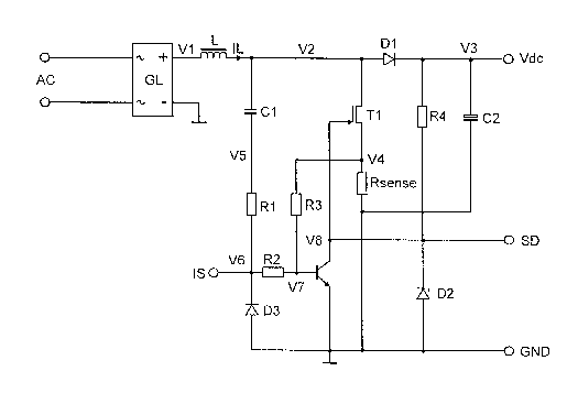
Figure 1 shows a step-up converter circuit. It is to be
considered part of an electronic ballast according to the
invention.
A voltage, which is supplied via an AC voltage input AC and is
rectified by a rectifier GL, is present at the circuit
arrangement between a node Vl and a reference potential GND.
A first series circuit comprising a storage inductor L, a diode
Dl and an intermediate circuit capacitor C2 is connected at the
output of the rectifier.
The connection between the storage inductor L and the diode Dl
represents a node V2. A series circuit comprising a switching
element T1 and a (measuring or shunt) resistor Rsense is
connected between the node V2 and the reference potential GND.
The switching element Tl can be in the form of a MOSFET. The
resistor Rsense is connected to the reference potential GND. A
node V8 is at the potential of the control input of the
switching element Tl.
A threshold value element T2 is connected between the control
input of the switching element Tl and the reference potential
CA 02605172 2007-10-16
13
GND. The threshold value element T2 can be in the form of a
(bipolar) transistor. There follows in the text below an
exemplary embodiment with a comparator as the threshold value
element. A node V7 is at the potential of the control input of
the threshold value element T2. A resistor R3 connects a node
V4 between T1 and Rsense to the node V7.
A series circuit comprising an output capacitor Cl, a resistor
Ri and a diode D3 is positioned between the node V2 and the
reference potential GND. A node V6 is positioned at the
connection between the resistor Rl and the diode D3.
A resistor R2 is positioned between the node V6 and the node
V7. A node V3 is positioned at the connection between the diode
Dl and the capacitor C2.
A series circuit comprising a resistor R4 and a diode D2 is
connected between the node V3 and the reference potential GND.
The connecting node between the diode D2 and the resistor R4 is
connected to the control input of the first switching element
Tl. The diode D2 is in the form of a Zener diode.
A signal line IS is connected to the node V6. Said signal line
can be set to the reference potential GND for a short period of
time by a control circuit.
A second signal line SD is connected to the control input of
the switching element Tl. The control circuit can block the
step-up converter using this signal line.
Figure 2a shows the potential at the node V6 and at the node V4
as a function of time. A current IL flows through the storage
inductor L. A voltage, which is proportional to the current IL
through the storage inductor L, is measured at the node V4 by
means of the resistor Rsense. The potential reflects the
magnetization state of the storage inductor L at the node V6.
This is ensured by the output capacitor Cl. If the storage
CA 02605172 2007-10-16
14
inductor is magnetized, the output capacitor Cl will discharge.
The potential at the node V6 in this case approximately
corresponds to the reference potential GND because it is caused
by the diode D3 to stick at a negative value with respect to
the reference potential GND which corresponds to the forward
voltage. If the storage inductor L is then demagnetized, the
output capacitor Cl is charged. A potential is formed at the
node V6 which is markedly above the reference potential GND.
The output capacitor Cl is dimensioned such that the time
constant comprising the capacitance Cl and the resistance Rl is
so great that complete charging of the output capacitor Cl does
not occur during the demagnetization of the storage inductor L,
in the time interval tb, and the potential at the node V6
remains above the switch-on threshold of the threshold value
element T2.
In figures 2a, b, c, intervals ta and tb and times tl and t2
are illustrated which correspond to the relevant time sections.
Figure 2b shows the current IL through the storage inductor L
as a function of time. Figure 2c shows the potential at the
node V7 as a function of time.
In the phase ta, the switching element Tl is switched on and
the threshold value element T2 is switched off. The potential
present at the node V4 increases proportionally to the current
IL through the storage inductor. The potential at the node V6
in this case approximately corresponds to the reference
potential GND. If the potential at the node V7, which is
connected to the node V4 via the resistor R3, exceeds the
switch-on threshold voltage of the threshold value element T2,
the threshold value element T2 is switched on and the switching
element Tl is switched off. The maximum current through the
step-up converter is therefore also limited. The corresponding
time t2 defines the end of the time interval ta.
CA 02605172 2007-10-16
After the time t2, there is the time interval tb. The threshold
value element T2 is switched on at time t2 indirectly by the
potential at the node V4 via the resistor R3. In this case, the
switching element Tl is switched off by the threshold value
element T2. At the node V6, the potential at time t2 jumps to a
value which is markedly above the reference potential GND. The
storage inductor is demagnetized during the time interval tb. A
current is flowing through Cl, R1 and R2 to the control input
of the threshold value element T2 and keeps said threshold
value element switched on as long as the demagnetization
current is flowing. The switching element T1 is switched off
since the potential at its control input no longer exceeds the
switch-on threshold.
The time interval tb ends with the complete demagnetization of
the storage inductor L. The potential at the node V2 therefore
jumps to the potential at the node V1 at the end of the time
interval tb. This jump defines the time tl and brings about,
via the output capacitor Cl, the resistor Ri and the diode D3,
a potential at the node V6 which approximately corresponds to
the reference potential GND. At the control input of the
threshold value element T2, the potential is no longer
sufficient for keeping the threshold value element T2 switched
on. It turns off.
The voltage across the intermediate circuit capacitor C2 now
switches the switching element Ti on via the resistor R4. A new
phase ta begins again. The high-frequency oscillation of the
step-up converter proceeds automatically.
In order to start the oscillation, it is possible to
distinguish between two cases. In the first case, the threshold
value element T2 is switched off and a sufficient voltage is
present at the intermediate circuit capacitor C2. Then, the
switching element Ti is switched on by the voltage across the
intermediate circuit capacitor via R4. In the second case, the
control circuit can set the voltage at the node V6 to the
CA 02605172 2007-10-16
16
reference potential GND for a short period of time via the
signal line IS. As a result, the switching element Tl is
switched on via the resistor R4.
The second case can occur if, when the supply voltage AC is
first applied, the capacitors Cl and C2 are charged parallel to
the potential Vl. The potential V6 then cannot fall below the
switch-on threshold voltage of the threshold value element T2
during a time which is considerably longer than the period
duration of the step-up converter. The threshold value element
T2 cannot be switched off until the charging of the
intermediate circuit capacitor C2 to the highest instantaneous
value of the supply voltage is complete. In this state, the
step-up converter is blocked by the threshold value element T2.
The control circuit can block the operation of the step-up
converter at any time via the signal line SD. This can take
place, for example, when a desired voltage is reached at the
intermediate circuit capacitor C2.
The threshold value element T2 has, in a circuit arrangement as
described above, a plurality of functions: a first function is
a threshold value element for detecting signals at the node V7;
the second function is driving the switching element Tl.
Furthermore, the threshold value element also functions as an
inverter.
In the circuit arrangement shown in figure 1, the resulting
maximum current through the storage inductor L is dependent on
the tolerance of the switching threshold of the threshold value
element T2.
Figure 3 shows a circuit diagram relating to a second circuit
arrangement according to the invention, which is improved in
this regard.
CA 02605172 2007-10-16
17
Instead of a transistor, a comparator AMP with a downstream
driver circuit TS is used as the threshold value element. Since
the comparator AMP cannot alone make available the power for
driving the switching element Tl, the driver circuit TS is
connected downstream of it. The comparator AMP receives a
separate voltage supply Vcc. A diode D4 is connected between
the node V6 and the positive supply potential Vcc. A capacitor
C3 can be connected in parallel with the resistor R2. This
accelerates the rise in the potential at the node V7 in the
event of a rise in the potential at the node V6 at the time tl
because it transfers the potential jump differentially. The
recharging of C3 takes place considerably more quickly than the
rise in the voltage at the node V7 as a result of the increase
in the current IL. The effect is already considered in
figure 2c. The capacitor C3 is illustrated in figure 3. A
resistor R5 for the supply voltage Vcc is connected between the
capacitor C3 and the resistor R3.
A switch-off threshold Vref is supplied to an input of the
comparator AMP. This switch-off threshold corresponds to the
switch-off criterion for the switching element Tl. It can be
fixed so as to be constant, but may also be variable, for
example proportionally to the profile of the input voltage AC.
The input of the comparator should not be subjected to
excessively high voltages. The event of the switching element
T1 being switched off at time t2 causes a voltage jump at the
node V7. In order to limit this jump, a diode V4 is connected
from the node V6 to the positive supply potential Vcc of the
comparator. As a result, the voltage at the node V6 is limited
to a potential which is higher than the supply potential Vcc of
the comparator by the forward voltage of the diode D4.
In order to reduce the sensitivity of the comparator to
interference, a so-called pull-up resistor R5 is connected
between the node V7 and the positive supply potential Vcc. The
potential at the node V7 is therefore raised away from the
CA 02605172 2007-10-16
18
reference potential. As a result, although the signal deviation
is reduced, the measure can nevertheless be advantageous
because the signal-to-noise ratio can be improved.
The introduction to the description describes the fact that it
may be desirable to set the parameters of the step-up converter
as a function of whether the electronic ballast is operated
using a phase gating dimmer or not. Firstly, a circuit
arrangement is proposed for identifying whether the ballast is
being operated using a phase gating dimmer or not. Then, this
circuit arrangement can be connected to the circuits from
figures 1 and 3 as described.
Figure 5 shows a circuit arrangement according to the invention
for identifying whether the electronic ballast is being
operated directly on the supply system or using a phase gating
dimmer. A capacitor CD is connected to one of the system feed
lines N or L as a differentiating element. A resistor RD, which
connects the capacitor CD to the reference potential GND, is
connected in series with this capacitor CD. At the node between
the capacitor CD and the resistor RD, the anode of a diode DS
is connected whose cathode is connected in series with a
further capacitor CS, likewise to the reference potential GND.
This circuit represents a peak value detection circuit of the
voltage occurring across the resistor RD. The base of a
transistor T is connected to the node between the capacitor CS
and the diode DS via a resistor RS. The emitter is connected to
the reference potential GND and the collector TC is connected
to elements of the step-up converter which can influence the
running of the step-up converter operation. Specific circuitry
is specified further below.
If the electronic ballast is connected directly to the system
supply, no substantial jumps in the supply voltage occur. The
component parts of the circuit arrangement in figure 5 are
designed such that the peak value of the voltage across RD is
CA 02605172 2007-10-16
19
stored in the capacitor CS via the diode DS and the voltage
across the capacitor CS cannot switch the transistor T on.
If the electronic ballast is connected to the supply system via
a phase gating dimmer, the supply voltage demonstrates
significant jumps. In this case, high peak values occur across
the resistor RD, so that the capacitor CS is charged to
significantly higher values in comparison with operation
without a phase gating dimmer. The voltage across the capacitor
CS can now change the transistor T over to a conductive state
via the resistor RS, whereby the collector-side output of the
transistor TC is approximately at the reference potential GND.
The step-up converter can be addressed via the output TC of the
transistor T, so that the switch-off current threshold is
reduced.
In figure 1, the switch-off current threshold is determined by
the resistors R2 and R3. If a resistor is switched from the
potential at the node V7 to the reference potential GND via the
switch T, the resulting desired value is greater if the switch
T is switched on.
In figure 3, the switch-off current threshold is determined by
the reference voltage Vref. The voltage Vref can be produced by
a voltage divider circuit comprising resistors. A resistor can
be connected in parallel with one of these resistors via the
switch T. The reference voltage Vref therefore changes by means
of the switch T being switched on and off.