Note : Les descriptions sont présentées dans la langue officielle dans laquelle elles ont été soumises.
CA 02605348 2007-10-16
WO 2006/116059 PCT/US2006/015055
NAN0'rYJBLSA8"M7CROWAVE FREQUENCY INTERCONNECTS
GOVERNMENT INFORMATION
This invention was made witli Government support under Grant No. N66001-03-1-
8914, awarded by the Office of Naval Research. The Government has certain
rights in this
invention.
FIELD OF THE INVENTION
The present invention relates to nanotubes and, more particularly, to the use
of
nanotubes to can.y currents and voltages at high frequencies.
BACKGROUND
Nanotubes are commonly made from carbon and comprise graphite sheets
seamlessly
wrapped into cylinders. Nanotubes can be single-walled or multi-walled. Single-
walled
nanotubes (SWNTs) comprise single cylinders and represent nearly ideal one
dimensional
electronic structures. Multi-walled nanotubes (MWNTs) comprise multiple
cylinders arranged
concentrically. Typical dimensions are 1-3 nm for SWNTs and 20-100 nm for
MWNTs.
Nanotubes can be either metallic or semiconducting depending on their
structure.
Metallic nanotubes are non-gateable, meaning that their conductance does not
change with
applied gate voltages, while semiconducting nanotubes are gateable. The
electrically properties
of nanotubes malce them promising candidates for the realization of nanoscale
electronic
devices smaller than can be achieved with current lithographic techniques.
Nanotube transistors are predicted to be extremely fast, especially if the
nanotubes can
be used as the interconnects themselves in future integrated nanosystems. The
extremely high
mobilities found in semiconducting nanowires and nanotubes are important for
high speed
operations, one of the main predicted advantages of nanotube and nanowire
devices in general.
Nanotubes may also have a role to play as high frequency interconnects in the
long term
between active nanotube transistors or in the short term between conventional
transistors
because of their capacity for large current densities.
Early theoretical work predicted significant frequency dependence in the
nanotube
dynamical impedance in the absence of scattering and contact resistance. The
origin of this
predicted frequency dependence is in the collective motion of the electrons,
which can be
thought of as one dimensional plasmons. Our equivalent circuit description
shows that the
nanotube forms a quantum transmission line, with distributed kinetic
inductance and both
quantum and geometric capacitance. In the absence of damping, standing waves
on this
-1-
CA 02605348 2007-10-16
WO 2006/116059 PCT/US2006/015055
traiismission line can give rise to resonant frequencies in the microwave
range (1-10 GHz) for
nanotube lengths between 10 and 100 nlm. We also proposed an ad-hoc damping
model,
relating the daniping to the dc resistance per unit length. To date, there
have been no
measurements of the microwave frequency conductance of a SWNT.
SUMMARY
The present invention provides nanotube interconnects capable of carrying
current and
voltage at high frequencies for use as high-speed interconnects in high
frequency circuits.
It is shown that the dynamical or AC conductance of single-walled nanotubes
equal
their DC conductance up to at least 10 GHz, demonstrating that the current
carrying capacity of
nanotube interconnects can be extended into the high frequency (microwave)
regime without
degradation. Thus, nanotube interconnects can be used as higli-speed
interconnects in high
frequeiicy circuits, e.g., RF and microwave circuits, and high frequency
nanoscale circuits. In a
preferred embodiment, the nanotube interconnects comprise metallic single-
walled nanotubes
(S)?VNTs), although otlier types of nanotubes may also be used, e.g., multi-
walled carbon
nanotubes (MWNTs), ropes of all metallic nanotubes, and ropes comprising
mixtures of
semiconducting and metallic nanotubes.
The nanotube interconnects are advantageous over copper interconnects
currently used
in integrated circuits. Nanotube interconnects have much higher conductivity
than copper
interconnects, and do not suffer from surface scattering, which can further
reduce the
conductivity of copper interconnects as dimensions are decreased below 100 nm.
The higher
conductivity of nanotube interconnects in addition to their demonstrated high
frequency current
carrying capacity make them advantageous over copper interconnects for high-
speed
applications, including high frequency nanoscale circuits.
The above and other advantages of einbodiments of this invention will be
apparent from
the following more detailed description when taken in conjunction with the
accompanying
drawings. It is intended that the above advantages can be achieved separately
by different
aspects of the invention and that additional advantages of this invention will
involve various
combinations of the above independent advantages such that synergistic
benefits may be
obtained from combined techniques.
BRIEF DESCRIPTION OF THE FIGURES
Figure 1 is a graph showing current-voltage characteristics for a device A, a
single-wall
nanotube (SWNT) with a 1 m electrode spacing.
-2-
CA 02605348 2007-10-16
WO 2006/116059 PCT/US2006/015055
rigure 2 is a grapn showirig"tihe conductance versus source-drain voltage for
device A at
frequencies of DC, 0.6 GHz, and 10 GHz.
Figure 3 is a graph showing current-voltage characteristics for a device B, a
SWNT
with an a 25 in electrode spacing.
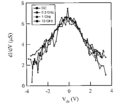
Figure 4 is a graph showing the conductance versus source-drain voltage for
device B at
frequencies of DC, 0.3 GHz, 1 GHz, and 10 GHz.
DETAILED DESCRIPTION
The present invention provides nanotube intercomiects capable of carrying
current and
voltage at high frequencies for use as high-speed intercoimects in high
frequency circuits. The
current and voltage carrying capacity of nanotube interconnects at high
frequencies is
demonstrated by the measurements below.
The first measurements of the high frequency conductance of a single-walled
nanotube
(SWNT) are presented. We find experimentally that the ac conductance is equal
to the dc
conductance up to at least 10 GHz. This clearly demonstrates for the first
time that the current
carrying capacity of carbon nanotubes can be extended without degradation into
the high
frequency (microwave) regime.
In our experimental results, no clear signatures of Tomonaga-Luttinger liquid
behavior
are observed (in the form of non-trivial frequency dependence) and no
specifically quantum
effects (reflecting quantuni versus classical conductance of nanotubes) are
reported, in
contradiction to theoretical predictions for ac conductance in ld systems that
neglect
scattering10. In order to explain this discrepancy between theory (which
neglects scattering) and
experiment (which includes realistic scattering), we present a
phenomenological model for the
finite frequency conductance of a carbon nanotube which treats scattering as a
distributed
resistance. This model explains why our results at ac frequencies do not
display fiequency
dependence. Simply put, resistive damping washes out the predicted frequency
dependence.
Individual SWNTs13 were synthesized via chemical vapor deposition14'1s on
oxidized,
high-resistivity p-doped Si wafers (p > 10 kSZ-cm) with a 400-500 nm Si02
layer. Metal
electrodes were formed on the SWNTs using electron-beam lithography and metal
evaporation
of 20-nm Cr/100 nm Au bilayer. The devices were not annealed. Nanotubes with
electrode
spacing of 1(device A) and 25 g.m (device B) were studied. Typical resistances
were - MS2;
some nanotubes had resistances below 250 kS2. In this study we focus on
metallic SWNTs
(defined by absence of a gate response) with resistance below 200 kS2.
Measurements were
performed at room temperature in air.
-3-
CA 02605348 2007-10-16
WO 2006/116059 PCT/US2006/015055
rig. I shows the room temperature I-V characteristic of device A, a SWNT with
a 1 m
electrode spacing. Since this length is comparable to the mean-free-path for
electrons, this
device is in the quasi-ballistic limit. The low-bias resistance of this device
was 60 kS2. This
resistance is most lilcely dominantly due to the contact; at low fields, once
electrons are injected
transport is quasi-ballistic from source to drain. The device clearly shows
saturation in the
current at around 20 A. The inset shows that (over almost the entire range of
applied voltage)
the absolute resistance (V/I) can be described by a simple function
V/I = Ro + IVI/Io Equation (1)
where Ro and Io are constants, as was originally found and explained by Yaol6.
From the slope
of the linear part of the R-V cuive, we find Io = 29 A for this device, in
good agreement with
Yao16 . There, it was shown that the saturation behavior is due to a modified
mean-free-path for
electrons when the electric field is suf.ficient to accelerate electrons to a
large enough energy to
emit an optical phonon. This effect was studied more quantitatively with
similar conclusions in
17,18
In order to measure the dynamical impedance at microwave frequencies, a
commercially available microwave probe (suitable for calibration with a
commercially
available open/short/load calibration standard) allowed for transition from
coax to
lithographically fabricated on chip electrodes. The electrode geometry
consisted of two small
contact pads, one 50x50 in2, and the other 200x200 n12 (for device A) or
50x200 m2 (for
device B). A microwave network analyzer is used to measure the calibrated
(complex)
reflection coefficient S t i(o)) =Vreflected/vincident, where Vineident is the
amplitude of the incident
microwave signal on the coax, and similarly for Vreeteeted. This is related to
the load impedance
Z(o)) by the usual reflection formula: S11= [Z(co)-50 S2]/[Z((o)+50 Q]. At the
power levels used
(3 W), the results are independent of the power used.
The statistical error in the measurement of both the Re(S11) and Im(S11) due
to random
noise in the networlc analyzer is less than 1 part in 104. A systematic source
of error in the
measurement due to contact-to-contact variation and non-idealities in the
calibration standard
gives rise to an error of 2 parts in 103 in the measurement of Re(S11) and
Im(S11). Because the
nanotube impedance is so large compared to 50 S2, these errors will be
important, as we discuss
in more depth below.
We measure the value of S11 as a function of frequency and source-drain
voltage for
both device A and B. While the absolute value of SI 1 is found to be 0~: 0.02
dB over the
frequency range studied (the systematic error due to contact-to-contact
variation), small
changes in Stl with the source-drain voltage are systematic, reproducible, and
well-resolved
-4-
CA 02605348 2007-10-16
WO 2006/116059 PCT/US2006/015055
witTiin the'stalist"ical err6'r of~'0:'0005 dB. The change in S11 with source-
drain voltage is not an
artifact, since coiztrol samples do not exhibit this effect. Our measurement
clearly shows that
the value of S 11, and hence the nanotube dynamical impedance, depends on the
dc source-drain
bias voltage, and that this dependence is independent of frequency over the
range studied for
both devices.
For both device A and B, we find Iin(S i~)= 0.000 0.002, indicating that the
nanotube
impedance itself is dominantly real. Our measurement system is not sensitive
to imaginary
impedances much smaller than the real impedance, which is of order 100 M. For
all
measurements presented here, Im(S 11) does not change with Vds within the
statistical
uncertainty of 1 part in 104. On the other hand, Re(S11) changes reproducibly
with Vds,
indicating that the real part of the nanotube dynamical impedance changes with
VdS.
By linearizing the relationship between S 11 and the conductance G, it can be
shown that
for small values of G (compared to 50 0), G(mS) =1.1 x S 11 (dB). (We note
that after
calibration, a control experiment with no nanotube gives 0 0.02 dB, where
the uncertainty is
due to variations in the probe location on the contact pads from contact to
contact.) Based on
this calculation, we conclude that the absolute value of the measured high
frequency
conductance is found to be 0 with an error of 22 S, which is consistent
witli the dc
conductance.
In order to analyze the data more quantitatively, we concentrate on the change
in S i
with Vds. The measurement error on the change in the ac conductance G with
bias voltage
depends primarily on the statistical uncertainty in S I,, which in our
experiments is 20 times
lower than the systematic error. (Since the contact probe remains fixed in
place while changing
the gate voltage, we can reproducibly and reliable measure small changes in S
11 with the
source-drain voltage.) Thus, although the absolute value of G can only be
measured with an
uncertainty of 20 S, a change in G can be measured with an uncertainty of 1
S. These
uncertainties are a general feature of any broadband microwave measurement
system.
Fig. 2 plots the conductance G vs. the source-drain voltage for device A at
dc, 0.6 GHz,
and 10 GHz. We only know the change in G with Vds, so we add an offset to Ga"
to equal Gd, at
Vds 0. We discuss this in more detail below, but at the moment it is clear
that the G at ac
changes with Vds just as it does at dc. We now discuss the offset.
Based on the measured results we know the absolute value of G is between 0 and
22
S; based on Fig. 2 we know that G changes by 10 S when Vds changes by 4 V.
The
dynamical conductance is probably not negative (there is no physical reason
for this to be the
case), which allows the following argument to be made: Since Gac(Vas 0)-
GaG(Vds 4V)=10 S
-5-
CA 02605348 2007-10-16
WO 2006/116059 PCT/US2006/015055
(measured), and Gac(Vds 4V) > 0 (on physical grounds), therefore GaxVds OV)>10
S; our
measurements put this as a lower limit; the upper limit would be 20 S.
Therefore, our
measurements show for the first time that, within 50%, nanotubes can carry
microwave
currents and voltages just as efficiently as dc currents and voltages.
Because device A is in the quasi-ballistic limit, but does not approach the
theoretical
lower limit of 6 kO for perfect contacts, the metal-nanotube contact
resistance probably
dominates the total resistance for this sample. In order to focus more heavily
on the nanotube
resistance itself, we turn now to device B.
Fig. 3 plots the I-V curve of a longer SWNT (device B), witli an electrode gap
of 25
m. (The original length of this nanotube was over 200 gm.) This device is
almost certainly
not in the ballistic limit, even for low-bias conduction, since the mean-free-
path is of order 1
mis,i7,1$ and the SWNT length is 25 m. The low-bias resistance of this device
is 1501cS2.
Previous measureinents in our lab15 on 4 mm long SWNTs gave a resistance per
unit length of
6 kS2/ m, indicating that the SWNT bulk resistance is about 150 kS2 for device
B, and that the
contact resistance is small compared to the intrinsic nanotube resistance. The
absolute
resistance (V/I) and the source-drain I-V curve for this device is well-
described by Equation
(1), as for device A. We find Io = 34 gA for this device, in agreement with
device A.
Fig. 4 plots the conductance G vs. the source-drain voltage for device B at
dc, 0.3 GHz,
1 GHz, and 10 GHz. As for device A, we only lcnow the change in G with Vds, so
we add an
offset to Gac to equal Gd,; at Vds 0. It is clear from this graph that the
nanotube dynamical
conductance changes with bias voltage just as the dc conductance does. Using
similar
arguments as for device A, our measurements for device B show that the ac and
dc conductance
are equal within 50% over the entire frequency range studied.
We now turn to a discussion of our results. At DC, the effects of scattering
on
nanotubes have been well-studied16-18. The dc resistance is given by19
11 I nnnoruve , Equation (2)
Rd - 4ez l,n.f.P.
where 1,,,,fp, is the mean-free-path. In ballistic systems, the sample contact
resistance dominates
and the dc resistance has a lower limit given by h/4e2 = 6 kS2, which is
possible only if electron
injection from the electrodes is reflectionless. Is Equation (2) true at
finite frequencies? The
answer to this question in general is not known.
For the simple case of an ohmically contacted nanotube of length L, we have
predicted
the first resonance would occur at a frequency given by vF/(4Lg), where vF is
the Fermi
velocity, L the length, and g the Luttinger liquid "g-factor", a parameter
which characterizes the
-6-
CA 02605348 2007-10-16
WO 2006/116059 PCT/US2006/015055
strengtn ot tne eiectron-electron interaction. Typically, g- 0.3. For L= 25
m, the first
resonance in the frequency dependent impedance would occur at 24 GHz, beyond
the range of
frequencies studied here. However, our nanotube for device B was originally
over 200 m
long. After deposition of electrodes, the nanotube extended under the two
electrodes for a
distance of at least 150 m on one side, and 50 m on the other. If these
segments of the
nanotube were intact, it would correspond to plasmon resonances at frequencies
of 4 and 8
GHz. We clearly do not observe any strong resonant behavior at these or any
other frequencies.
We believe this must be dtie to the damping of these plasmons, as we discuss
below.
While this is not justified rigorously, we assume that Equation (2) describes
a
distributed resistance of the nanotube that is independent of frequency, equal
to the measured
dc resistance per unit length of 61cS2/ m of similar long nanotubes grown in
our lab ' 5. In our
previous modeling worlcl l, we found that (under such heavy danzping
conditions) the nanotube
dynamical impedance is predicted to be equal to its dc resistance for
frequencies less than
1/(27CR&Ctotal), where Ctotal is the total capacitance of the nanotube
(quantum and electrostatic).
Although our measurements presented here are on top of a poorly conducting
ground plane
(high resistivity Si), and the previous modeling worlc was for a highly
conducting substrate, we
can use the modeling as a qualitative guide. For device B, we estimate Ctota1=
1 fF, so that the
ac impedance would be predicted to be equal to the dc resistance for
frequencies below about -
1 GHz. This is qualitatively consistent with what we observe experimentally.
At high bias voltages, the electrons have enough energy to emit optical
phonons,
dramatically reducing the mean-free-path and modifying Equation (2) to the
more general
Equation (1). Our measurements clearly show that Equation (1) is still valid
up to 10 GHz. A
theoretical explanation for this is lacking at this time, although it is
intuitively to be expected
for the following reason: the electron-phonon scattering frequency in the high-
bias region is
approximately 1 THz18. Therefore, on the time-scale of the electric field
period, the scattering
frequency is instantaneous. Further theoretical worlc is needed to clarify
this point.
Measurements up to higher fiequencies of order the electron-phonon scattering
rate
50 GHz at low electric fields' 8) should allow more information to be learned
about electron-
phonon scattering in nanotubes; temperature dependent measurements would allow
for more
information as well, such as the intrinsic nanotube inipedance at low
scattering rates.
Therefore, it has been verified experimentally that the dynamical iinpedance
of metallic
SWNTs are dominantly real and frequency independent from dc to at least 10
GHz. As a
result, the high current carrying capacity of metallic SWNTs does not degrade
into the high
frequency (microwave) regime allowing SWNTs to be used as high-speed
interconnects in
-7-
CA 02605348 2007-10-16
WO 2006/116059 PCT/US2006/015055
higti-speed applications "Tri'the preterred embodiment, the nanotube
interconnects comprise
metallic SWNTs, although other types of nanotubes may also be used, e.g.,
MWNTs, ropes of
all metallic nanotubes, and ropes comprising mixtures of semiconducting and
metallic
nanotubes. Metallic SWNTs can have a very high current density (of order 109
A/cm). A
metallic SWNT of order 1-3 nni in diameter can carry currents and voltages of
up to 25 A or
higher.
Therefore, nanotube interconnects can be used as high-speed interconnects in a
variety
of high frequency applications. For exainple, nanotube interconnects can be
used to provide
high-speed interconnects in computer processors operating at high clock
frequencies of 1 GHz
or higher. Nanotubes interconnects can also be used to provide high-speed
interconnects in
radio frequency (RF) and microwave circuits operating at frequencies up to 10
GHz or higher
such as in cellular phones and wireless networlc systems. The nanotube
interconnects can be
used to intercomiect active devices (e.g., transistors), passive devices, or a
combination of
active and passive devices in circuits operating at high frequencies in the
GHz range. The
nanotube interconnects can also be used to interconnect nanoscale devices to
realize high
frequency all nanotube circuits. For example, the nanotube interconnects can
be used to
interconnect nanotube field effect transistors (FETs), in which semiconducting
nanotubes are
used for the channels of the nanotube FETs. The nanotube intercoimects can
also be used to
interconnect lager-scale devices, e.g., conventional transistors, for high-
speed applications or to
interconnect a combination of nanoscale and larger-scale devices in a circuit.
A nanotube
interconnect can coinprise a single nanotube or comprise more than one
nanotube arranged in
parallel in an N-array, where N is the number of nanotubes.
The invention also provides a useful method for modeling nanotube
interconnects in
circuit simulation programs used for designing high frequency circuits. In an
embodiment, a
circuit siinulation program models the dynamical impedance of nanotube
interconnects in high
frequency circuits as being equal to their dc resistance. In other words, the
circuit simulation
program assumes that the dc resistance of the nanotube interconnect dominates
at high
frequencies and that the dynamical impedance is not sensitive to imaginary
impedances
(inductances and capacitances).
The nanotube intercoimects are advantageous over copper interconnects
currently used
in integrated circuits. When scaled by the diameter of 1.5 nm, the resistance
per unit length of
a nanotube we measure gives a resistivity conductivity of 1 52-cm, which is
lower than that of
bulk copper. In addition, copper interconnects typically suffer increased
surface scattering as
the dimensions are decreased below 100 nm, so that even the bulk conductivity
of copper is not
-8-
CA 02605348 2007-10-16
WO 2006/116059 PCT/US2006/015055
-'reffizbd'ati"ti'lifft leiigtli saalC''' trl' ariaYtion, the current density
of carbon nanotubes exceeds that
of copper. Tllus, per unit widtli, carbon nanotubes are superior materials to
copper as
interconnects in integrated circuits.
Our equivalent circuit description shows that the nanotube forrns a quantum
transmission line, with distributed kinetic inductance and both quantuin and
geometric
capacitance. The lcinetic inductance for an individual nanotube is about 4 nH/
m. Numerically
this gives rise to an indt-ctive iinpedance of iaoL, where L is the
inductance. However, the
resistance per unit length is about 6 kSZ/ m. This means that the resistive
impedance will
dominate the inductive impedance at frequencies below about 200 GHz for a
single walled
nanotube. Therefore, when considering the applications of nanotubes as
interconnects at
microwave frequencies, the resistance should be the dominant consideration.
However, the conductivity of nanotubes is larger than copper. Arraying
nanotubes
allows for wiring with less resistance per unit length than copper of the same
total cross
sectional area. In addition, the kinetic inductance of an N-array of nanotubes
is N times lower
than the kinetic inductance of an individual nanotube.
In sum, for nanotubes resistance is the dominate circuit component (as opposed
to
inductance), and this resistance is smaller than copper wires of the same
dimensions. Therefore
kinetic inductance is not a inajor "show-stopper" for the use of nanotubes as
interconnects. In
addition, there is no cross-talk between nanotubes due to kinetic inductance.
This is in contrast
to magnetic inductance in copper, which induces cross-talk. Therefore,
considering all these
factors, carbon nanotubes is superior to copper in all aspects of circuit
performance.
While the invention is susceptible to various modifications, and alternative
forms,
specific examples thereof have been shown in the drawings and are herein
described in detail.
It should be understood, however, that the invention is not to be limited to
the particular forms
or methods disclosed, but to the contrary, the invention is to cover all
modifications,
equivalents and alternatives falling within the spirit and scope of the
appended claims.
-9-
CA 02605348 2007-10-16
WO 2006/116059 PCT/US2006/015055
REFERENCES
P. L. McEuen, M. S. Fuhrer, and H. K. Park, "Single-walled carbon nanotube
electronics," Ieee T Nanotechnol 1 (1), 78-85 (2002).
2 M. Bockrath, D. H. Cobden, J. Lu, A. G. Rinzler, R. E. Smalley, T. Balents,
and P. L.
McEuen, "Luttinger-liquid behaviour in carbon nanotubes," Nature 397 (6720),
598-601
(1999); M.P.A. Fisher and L.I. Glazman, in Mesoscopic Electron Transport,
edited by Lydia L.
Sohn, Leo P. Kouwenhoven, Gerd Scheon et al. (Kluwer Academic Publishers,
Dordrecht ;
Boston, 1997).
3 A. Javey, J. Guo, Q. Wang, M. Lundstrom, and H. J. Dai, "Ballistic carbon
nanotube
field-effect transistors," Nature 424 (6949), 654-657 (2003).
4 H. W. C. Postnia, T. Teepen, Z. Yao, M. Grifoni, and C. Dekker, "Carbon
nanotube
single-electron transistors at room temperature," Science 293 (5527), 76-79
(2001).
5 K. Tsukagoshi, B. W. Alphenaar, and H. Ago, "Coherent transport of electron
spin in a
ferromagnetically contacted carbon nanotube," Nature 401 (6753), 572-574
(1999).
6 P.J. Burlce, "AC Perfonnance of Nanoelectronics: Towards a THz Nanotube
Transistor," Solid State Electronics 40 (10), 1981-1986 (2004); S. Li, Z. Yu,
S. F. Yen, W. C.
Tang, and P. J. Burke, "Carbon nanotube transistor operation at 2.6 GHz," Nano
Lett 4 (4),
753-756 (2004).
7 Y. Cui, Z. H. Zhong, D. L. Wang, W. U. Wang, and C. M. Lieber, "High
performance
silicon nanowire field effect transistors," Nano Lett 3 (2), 149-152 (2003).
8 T. Durkop, S. A. Getty, E. Cobas, and M. S. Fuhrer, "Extraordinary mobility
in
semiconducting carbon nanotubes," Nano Lett 4 (1), 35-39 (2004).
9 "International Technology Roadmap for Semiconductors,
http://public.itrs.net/," (2003).
10 Y. M. Blaiiter, F. W. J. Heldcing, and M. Buttiker, "Interaction constants
and dynamic
conductance of a gated wire," Phys Rev Lett 81 (9), 1925-1928 (1998); V. V.
Ponomarenko,
"Frequency dependences in transport through a Tomonaga-Luttinger liquid wire,"
Phys Rev B
54 (15), 10328-10331 (1996); V. A. Sablikov and B. S. Shchamlchalova, "Dynamic
conductivity of interacting electrons in open mesoscopic structures," Jetp
Lett+ 66 (1), 41-46
(1997); G. Cuniberti, M. Sassetti, and B. Kramer, "Transport and elementary
excitations of a
Luttinger liquid," J Phys-Condens Mat 8 (2), L21-L26 (1996); G. Cuniberti, M.
Sassetti, and B.
Kramer, "ac conductance of a quantum wire with electron-electron
interactions," Phys Rev B
57 (3), 1515-1526 (1998); I. Safi and H. J. Schulz, "Transport in an
inhomogeneous interacting
one-dimensional system," Phys Rev B 52 (24), 17040-17043 (1995); V. A.
Sablikov and B. S.
-10-
CA 02605348 2007-10-16
WO 2006/116059 PCT/US2006/015055
Shcliairilchalova, "I7yhaiii'iC"'ffMsP'ot't of interacting electrons in a
mesoscopic quantum wire," J
Low Temp Phys 118 (5-6), 485-494 (2000); R. Tarlciainen, M. Ahlskog, J.
Penttila, L.
Roschier, P. Halconen, M. Paalanen, and E. Sonin, "Multiwalled carbon
nanotube: Luttinger
versus Fenni liquid," Phys Rev B 64 (19), art. no.-195412 (2001); C. Roland,
M. B. Nardelli, J.
Wang, and H. Guo, "Dynamic conductance of carbon nanotubes," Phys Rev Lett 84
(13), 2921-
2924 (2000).
11 P. J. Burlee, "An RF Circuit Model for Carbon Nanotubes," Ieee T
Nanotechnol 2 (1),
55-58 (2003); P. J. Burke, "Luttinger liquid theory as a model of the
gigahertz electrical
properties of carbon nanotubes," Ieee T Nanotechnol 1 (3), 129-144 (2002).
12 P. J. Burlce, I. B. Spielman, J. P. Eisenstein, L. N. Pfeiffer, and K. W.
West, "High
frequency conductivity of the high-mobility two-dimensional electron gas,"
Appl Phys Lett 76
(6), 745-747 (2000).
13 M. J. Biercuk, N. Mason, J. Martin, A. Yacoby, and C. M. Marcus, "Anomalous
conductance quantization in carbon nanotubes," Phys Rev Lett 94 (2), - (2005);
(Similarly,
altliough it is possible we are measuring small ropes or double walled tubes,
most likely we
have a single metallic tube. TEM images of nanotubes grown under similar
conditions showed
only single-walled nanotubes.)
14 J. Kong, H. T. Soh, A. M. Cassell, C. F. Quate, and H. J. Dai, "Synthesis
of individual
single-walled carbon nanotubes on patterned silicon wafers," Nature 395
(6705), 878-881
(1998); Zhen Yu, Shengdong Li, and P. J. Burlce, "Synthesis of Aligned Arrays
of Millimeter
Long, Straigllt Single Walled Carbon Nanotubes," Cheinistry of Materials 16
(18), 3414-3416
(2004).
15 Shengdong Li, Zhen Yu, and P. J. Burke, "Electrical properties of 0.4 cm
long single
walled carbon nanotubes," Nano Lett 4 (10), 2003-2007 (2004).
16 Z. Yao, C. L. Kane, and C. Dekker, "High-field electrical transport in
single-wall
carbon nanotubes," Phys Rev Lett 84 (13), 2941-2944 (2000).
17 A. Javey, J. Guo, M. Paulsson, Q. Wang, D. Mann, M. Lundstrom, and H. J.
Dai,
"High-field quasiballistic transport in short carbon nanotubes," Phys Rev Lett
92 (10), - (2004).
18 J. Y. Park, S. Rosenblatt, Y. Yaish, V. Sazonova, H. Ustunel, S. Braig, T.
A. Arias, P.
W. Brouwer, and P. L. McEuen, "Electron-phonon scattering in metallic single-
walled carbon
nanotubes," Nano Lett 4 (3), 517-520 (2004).
19 Supriyo Dafta, Electronic trarasport in mesoscopic systenas. (Cambridge
University
Press, Cambridge ; New York, 1995), pp.xv, 377 p.
-11-