Note : Les descriptions sont présentées dans la langue officielle dans laquelle elles ont été soumises.
CA 02607599 2007-11-06
WO 2006/124270 PCT/US2006/016796
-1-
RADIO FREQUENCY IDENTIFICATION TAGS FOR USE ON METAL OR
OTHER CONDUCTIVE OBJECTS
TECHNICAL FIELD
The present invention relates to radio frequency identification ("RFID") tags
that
are useful on metal or other conductive objects and to methods for
manufacturing the
same. The present invention relates more particularly to a radio frequency
identification
tag, including: a substrate including a first major surface and a second major
surface
opposite the first major surface; a radio frequency identification antenna
attached to the
first major surface of the substrate; an integrated circuit attached to the
antenna; and a first
composite layer.
BACKGROUND OF THE INVENTION
Various methods have been developed to help reduce or eliminate interference
problems when a radio frequency identification ("RFID") tag is proximate or
adjacent a
conductive object, such as a metal object. Using some of these methods, it is
possible for
an RFID reader to properly read the RFID tag, despite its location next to the
conductive
object. Examples of such methods are disclosed in the following publications
and patent:
PCT Publication WO 03/030093 (Gschwindt), "Transponder Label and Method for
the
Production Thereof;" PCT Publication WO 03/067512 (Surkau), "Transponder
Label;"
and U.S. Pat. No. 6,371,380 (Tanimura), "Non-Contacing-Type Information
Storing
Device. In addition, there are commercially available spacer materials for use
in RFID
tags to help reduce or eliminate interference problems. For example, one type
of
commercially available material is broadband absorbers available from Emerson
&
Cuming based in Randolph, MA under the trade name ECCOSORB.
SUMMARY OF THE INVENTION
One embodiment of the present invention provides a radio frequency
identification
RFID tag. In this embodiment, the RFID tag comprises: a substrate including a
first major
surface and a second major surface opposite the first major surface; a radio
frequency
CA 02607599 2007-11-06
WO 2006/124270 PCT/US2006/016796
-2-
identification antenna attached to the first major surface of the substrate;
an integrated
circuit attached to the antenna; and a first composite layer including a first
major surface
and a second major surface opposite the first major surface, wherein the first
composite
layer is attached to the second major surface of the substrate, wherein the
first composite
layer comprises: binder; and a plurality of multilayered flakes dispersed in
the binder, the
multilayered flakes comprising two to about 100 layer pairs, each layer pair
comprising:
one crystalline ferromagnetic metal layer, adjacent to one dielectric layer
wherein the layer
pairs form a stack of alternating ferromagnetic metal layers and dielectric
layers.
Another embodiment of the present invention provides a method of manufacturing
a radio frequency identification ("RFID") tag. In this embodiment, the method
comprises
the steps of: providing a substrate containing an antenna on at least one
surface of the
substrate; attaching an integrated circuit to the antenna; providing a first
composite layer
including a first major surface and a second major surface opposite the first
major surface,
wherein the first composite layer is attached to the second major surface of
the substrate,
wherein the first composite layer comprises: binder; and a plurality of
multilayered flakes
dispersed in the binder, the multilayered flakes comprising two to about 100
layer pairs,
each layer pair comprising: one crystalline ferromagnetic metal layer adjacent
to one
dielectric layer, wherein the layer pairs form a stack of alternating
ferromagnetic metal
layers and dielectric layers; and attaching the first composite layer to the
substrate
opposite the antenna and integrated circuit.
BRIEF DESCRIPTION OF THE DRAWINGS
The present invention will be further explained with reference to the appended
Figures, wherein like structure is referred to by like numerals throughout the
several
views, and wherein:
Figure 1 is a top view of a typical radio frequency identification ("RFID")
tag
known in the art;
Figure 2 is a schematic view of interactions between the RFID tag of Figure 1
and
a RFID reader;
Figure 3 illustrates the interaction between the RFID tag of Figure 1 and a
conductive object;
CA 02607599 2007-11-06
WO 2006/124270 PCT/US2006/016796
-3-
Figure 4 illustrates the interaction between the RFID tag and conductive
object of
Figure 3 and prior art spacers;
Figure 5 is a side view of one embodiment of the RFID tag of the present
invention;
Figure 6 is a side view of anotlier embodiment of the RFID tag of the present
invention;
Figure 7 is a view along line 7-7 in Figure 5 illustrating yet another
embodiment of
the RFID tag of the present invention;
Figure 8 is a view similar to the view of Figure 7 illustrating another
embodiment
of the RFID tag of the present invention; and
Figure 9 is a view similar to the view of Figure 7 illustrating yet another
embodiment of the RFID tag of the present invention.
DETAILED DESCRIPTION OF THE INVENTION
I. RFID Tags and Readers.
This section describes typical radio frequency identification ("RFID") tags
and
readers, as are well known in the art. Figure 1 illustrates a typical radio
frequency
identification ("RFID") tag 10. The RFID tag 10 includes a substrate 12 having
a first
major surface 14 and a second major surface 16 opposite the first major
surface 14.
Preferably the substrate 12 is a flexible substrate, such that it could be
used in a label that
may be wrapped around an object. The flexible substrate 12 could have enough
flexibility
to conform to a variety of surfaces and bend easily around objects. For
example, the
substrate 12 is preferably in the range of 25-100 microns in thickness, and is
made of a
flexible material, such as polyester, polyethylene naphthanate, polyimide,
polypropylene,
paper, or other flexible materials apparent to those skilled in the art.
An RFID element is attached to the first major surface 14 of the substrate 12.
The
RFID element typically includes two major components: an integrated circuit 20
and an
antenna 18. The integrated circuit 20 provides the primary identification
function. It
includes software and circuitry to permanently store the tag identification
and other
desirable information, interpret and process commands received from the
interrogation
CA 02607599 2007-11-06
WO 2006/124270 PCT/US2006/016796
-4-
hardware, respond to requests for information by the interrogator, and assist
the hardware
in resolving conflicts resulting from multiple tags responding to
interrogation
simultaneously. Optionally, the integrated circuit may provide for updating
the
information stored in its memory (read/write) as opposed to just reading the
information
out (read only). Integrated circuits suitable for use in RFID tags 10 include
those available
from Texas Instruments (in their line of products under the trade names TIRIS
or TAG-
IT), Philips (in their line of products under the trade names I-CODE, MIFARE
and
HITAG), among others.
The antenna 18 geometry and properties depend on the desired operating
frequency
of the RFID tag 20. For example, 915 MHz or 2.45 GHz RFID tags 10 would
typically
include a dipole antenna, such as a linear dipole antenna or a folded dipole
antenna. A
13.56 MHz (or similar) RFID tag 10 would typically use a spiral or coil
antenna 18, as
shown in Figure 1. However, other antenna designs are known to those skilled
in the art.
In either case, the antenna 18 intercepts the radio frequency energy radiated
by an
interrogation source, such as the RFID reader 60 illustrated schematically in
Figure 2.
(Reference number 62 illustrates the radio frequency energy radiated by the
RFID reader
60.) This signal energy 62 carries both power and commands to the tag 10. The
antenna
enables the RF-responsive element to absorb energy sufficient to power the
integrated
circuit 20 and thereby provide the response to be detected. Thus, the
characteristics of the
antenna must be matched to the system in which it is incorporated. In the case
of tags
operating in the high MHz to GHz range, the most important characteristic is
the antenna
length. Typically, the effective length of a dipole antenna is selected so
that it is close to a
half wavelength or multiple half wavelength of the interrogation signal. In
the case of tags
operating in the low to mid MHz region (13.56 MHz, for example) where a half
wavelength anteima is impractical due to size limitations, the important
characteristics are
antenna inductance and the number of turns on the antenna coil. Typically,
metals such as
copper or aluminum would be used, but other conductors, including printed
inks, are also
acceptable. It is also important that the input impedance of the selected
integrated circuit
match the impedance of the antenna for maximum energy transfer. Additional
information
about antennas is known to those of ordinary skill in the art, for example, in
reference
texts such as RFID Handbook Radio-Frequency Identification Fundamentals and
CA 02607599 2007-11-06
WO 2006/124270 PCT/US2006/016796
-5-
Applications, by K. Finkenzeller, (1999 John Wiley & Sons Ltd, Chichester,
West Sussex,
England).
A capacitor 22 is often included to increase the performance of the RFID tag
10.
The capacitor 22, when present, tunes the operating frequency of the tag to a
particular
value. This is desirable for obtaining maximum operating range and insuring
compliance
with regulatory requirements. The capacitor may either be a discrete
component, or
integrated into the antenna 18.
An RFID reader or interrogator 60 is schematically illustrated in Figure 2.
The
RFID reader 60 includes an RFID reader antenna 64. RFID readers 60 are well
lcnown in
the art. For example, commercially available RFID readers are available from
3M
Company based in St. Paul, as the 3MT"" Digital Library Assistant as model
numbers 702,
703, 802, and 803. Another example of a commercially available RFID reader is
a model
IP3 portable RFID (UHF) Reader attached to an IntermecTM 700 Series Mobile
computer
available from Intermec Technologies Corporation, Everett, WA.
The RFID reader 60 and RFID tag 10 form an RFID system. Inductively coupled
RFID systems are based on near-field magnetic coupling between the antenna
loop of the
RFID reader and the antenna coil of the RFID transponder, according to RFID
Handbook,
Radio-Frequency Identification Fundamentals and Applications, by K.
Finkenzeller, (1999
John Wiley & Sons Ltd, Chichester, West Sussex, England) pp. 21. A number of
RFID
systems are available, following one of several communication and system
performance
standards. The discussion below is principally based on RFID systems operating
at 13.56
MHz, but the discussion extends to inductively coupled RFID systems at other
operating
frequencies.
II. Interference Problems When RFID Tags are in Close Proximity with
Conductive
Objects.
This section describes the typical interactions between RFID tags and RFID
readers, and the interference problems typically encountered when RFID tags
are in close
proximity to conductive objects. Figure 2 illustrates the RFID reader 60
interrogating an
RFID tag 10 that is not located close to a conductive object. Figure 3
illustrates the
interrogation of an RFID tag 10 in close proximity to a conductive object 24.
Examples of
CA 02607599 2007-11-06
WO 2006/124270 PCT/US2006/016796
-6-
conductive objects 24 include objects containing metal, nonmetallic substances
(e.g.,
carbon-fiber based composite), or liquid (e.g., an aqueous ionic solution in a
bottle). For
example, a conductive object could include a metal airplane part or tool.
Figure 4
illustrates the interrogation of the RFID tag 10 in close proximity to the
conductive object
24 with a prior art spacer layer 66 located between the RFID tag 10 and the
conductive
object 24.
As illustrated in Figure 2, the RFID reader 60 interrogates the RFID tag 10
and as a
consequence, the RFID reader 60 produces a time-varying electrical current in
the RFID
reader antenna 18. The variations in electrical current may be the smoothly
varying
sinusoidal carrier frequency, or the variations may be aperiodic and non-
repetitive
variations in amplitude, frequency, or phase of the sinusoidal carrier
frequency
representing encoded digital data. The time-varying electrical current
produces a
electromagnetic field, which extends through space to the RFID antenna 18. The
time-
varying magnetic flux through the RFID antenna 18 induces an electromotive
force (EMF)
in the RFID antenna 18, according to Faraday's Law of Induction, which is
described in
more detail in Electroma ng etism by John C. Slater and Nathaniel H. Frank, ,
(1969 Dover
Publications, New York), pp. 78-80. The induced EMF appears as an effective
induced
voltage across the two end terminals of the RFID antenna 18, hence giving the
classification lcnown in the art as an "inductively coupled RFID system." The
induced
voltage drives a time-varying electrical current through the RFID integrated
circuit 20,
thereby completing the RFID communication link from the RFID reader 60 to the
RFID
tag 10.
When, as illustrated in Figure 3, the RFID antenna 18 is not in free space,
but is
adjacent to an item with finite electrical conductivity, such as a conductive
object 24, the
EMF induced in the RFID transponder antenna is reduced, generally to a level
at which
the tag is not able to respond. This occurs when situations such as that
illustrated by
Figure 3 occur, i.e. when the plane of the RFID antenna 18 is substantially
parallel with
and proximate to the surface of the conductive object 24. This might be the
case if, for
example, the RFID tag 10 is attached to the conductive object 24 as a label to
identify the
object. According to Faraday's Law of Induction, eddy currents will be induced
in the
conductive object, as discussed in more detail in Electromagnetism by John C.
Slater and
Nathaniel H. Franlc,,(1969 Dover Publications, New York) pp.78-80. According
to
CA 02607599 2007-11-06
WO 2006/124270 PCT/US2006/016796
-7-
Lenz's Law, the net effect of the eddy currents is to reduce the magnetic flux
near the
conductive object, as discussed in more detail in the RFID Handbook. Radio-
Frequency
Identification Fundamentals and Applications, by K. Finkenzeller, (1999 John
Wiley &
Sons Ltd, Chichester, West Sussex, England) p.64. The reduced net magnetic
flux near
the conductive object results in a reduced EMF in the RFID transponder
antenna,
compared to the first case illustrated in Figure 2, where the RFID antenna 18
was in free
space.
If the RFID reader 60 is transmitting a time-varying electromagnetic field,
the
RFID tag 10 will intercept this time-varying electromagnetic field. As a
consequence of
the RFID tag 10 being adjacent the conductive object 24, an EMF is induced in
the RFID
antenna 18 and an induced electrical current circulates in the RFID integrated
circuit 20, as
described above. The electrical current circulating in the RFID tag 10 will
induce an eddy
current in the substrate of the conductive object 24. The magnitude of the
induced eddy
current depends in part on the amount of electromagnetic energy reaching the
conductive
substrate. If this amount of electromagnetic energy is decreased, the
magnitude of the
induced eddy current in the conductive object will proportionately decrease.
If the antenna 18 of the RFID tag 10 is a rectilinear antenna, as illustrated
in Figure
4, then the conductors that comprise the antenna 18 are essentially long
straight
conductors, connected at each end to adjacent conductors to form a loosely
coiled.antenna
form. The electrical current I in each long straight portion of each conductor
in the RFID
antenna 18 sets up a magnetic field H at a distance r away from each portion
respectively,
where ,uo is the permeability in free space according to the following
formula:
H = ,uoI/( 2 7x)
If the RFID tag 10 is proximate or adjacent to the conductive object 24, the
magnetic
fields generated by each conductor segment will induce a counter-circulating
eddy current
in the conductive object 24, as illustrated by the clockwise arrow. The
strength of the
induced eddy current depends on the amount of magnetic field energy coupled
into the
conductive substrate. If the RFID tag 10 is attached to the conductive object
10, for
example by a thin layer of adhesive, the energy coupled from the RFID tag 10
to the
conductive object 24 will be large and the induced eddy current will be
correspondingly
large. If the eddy current is similar in magnitude to the RFID tag 10 current,
but opposite
CA 02607599 2007-11-06
WO 2006/124270 PCT/US2006/016796
-8-
in direction, the sum of the transponder current and the eddy current will be
essentially
zero and the RFID tag 10 will not be detected by the RFID reader 60. This
physical
phenomenon is often referred to by those skilled in the art as "interference
problems"
when RFID tags are in close proximity with conductive objects such as metal
objects.
Various methods are lcnown by those skilled in the art to help reduce or
eliminate
the interference problems described above when an RFID tag is proximate or
adjacent a
conductive object. Using some of these methods, it is possible for an RFID
reader to
properly read the RFID tag, despite its location next to the conductive
object. Various
methods described in the prior art literature may be used to
electromagnetically decouple
the RFID transponder from the conductive surface. Examples of such methods are
disclosed in the following publications and patent: PCT Publication WO
03/030093
(Gschwindt), "Transponder Label and Method for the Production Thereof,"; PCT
Publication WO 03/067512 (Surkau), "Transponder Label"; and U.S. Pat. No.
6,371,380
(Tanimura), "Non-Contacing-Type Information Storing Device. WO 03/030093
describes
a shielding layer that has ferrite particles embedded therein. WO 03/067512
also
describes a shielding film that has ferrite particles embedded therein.
Ferrite particles are
inorganic compounds containing iron in one of its natural oxidation states
(Fe3+)
chemically bound with oxygen and other chemical elements. Typically, the
ferrite
particles are uniform in composition throughout the particle, and homogenous,
for
example, the ferrite compound is the same throughout the full depth of the
particle. U.S.
Pat. No. 6,371,380 describes using a magnetism absorbing plate formed from
Sendust.
Although not stated in the '380 patent, it is known in the industry that
Sendust is made
from a ferrous alloy powder. The base material is approximately 85% iron, 6%
aluminum,
and 9% silicon. (See for example Soft Magnetics Application Guide published by
Arnold
Magnetic Technologies Corporation, Rochester, NY, p. 30-1, February 2003 Rev.
B.)
Figure 4 illustrates an example of these prior art methods. As illustrated in
Figure
4, the RFID tag 10 is electromagnetically decoupled from the surface of the
conductive
object 24. A ferrite shield 66 is placed between the RFID antenna 18 and the
conductive
object surface 24. The RFID tag 10 may be attached to an electromagnetic
ferrite shield
66, which may in turn be attached to the surface of the conductive object 24.
The ferrite
shield 66 will minimize the occurrence of eddy currents induced in the
conductive object
24 and the consequent reduction of induced EMF in the RFID antenna 18, as
illustrated
CA 02607599 2007-11-06
WO 2006/124270 PCT/US2006/016796
-9-
graphically in Figure 4. In other words, the electromagnetic ferrite shield 66
is not
electrically conductive, so it will not support eddy currents in the presence
of a time-
varying magnetic field. It is noted too that the proximity of the ferrite
material may load
the antenna 18 and increase its inductance to such a degree that the resonant
frequency of
the RFID tag 10 will need to be adjusted. (Klaus Finkenzeller, RFID Handbook,
John
Wiley & Son, Ltd., Chichester (1999), pp. 101-102.) A further claimed
advantage of
ferrites is the high electrical resistivity, on the order of 1 x 10⁶ 52-m,
compared to metallic
resistivity in the range of 1 x 10"5 to 1 x 10"4 S2-m. Because of the
intrinsic high resistivity
of ferrite materials, eddy currents are not a factor and consequently the loss
of energy in
eddy currents is also low. Other prior art methods teach RFID transponders
wound on
ferrite cores and encased in plastic designed to mark tools and metal gas
bottles. (Klaus
Finkenzeller, RFID Handbook, John Wiley & Son, Ltd., Chichester (1999), pp. 16-
17.)
One of the disadvantages of the approach that uses the shields with ferrite
particles
or other iron-based, magnetic particulates embedded in such shields to help
reduce or
eliminate the interference problems described above is that often these
shields will
contribute a large ainount of mass or weight to the overall RFID tag. Ferrites
are typically
heavy, bulky, and rigid. In addition, such shields will often have a
relatively high areal
density (i.e., mass per unit area) and tend to be much thicker than other
materials typically
found in an RFID tag. In particular applications, this additional weight or
additional
thickness added to the RFID tags tends to be disadvantageous. For example, if
particular
parts in an airplane have an RFID tag with a ferrite shield attached to them,
the resulting
increase in weight added to the airplane may affect how the airplane
ultimately functions.
Boeing and Airbus propose to use RFID labels to track their airplane parts to
improve maintenance and replacement services. It is proposed that passive RFID
tags be
attached to removable parts on new jets. The RFID labels may contain
information stored
on the integrated chip related to the part it is attached to, for example,
part and serial
numbers, manufacturer codes, country of origin, date of installation and
maintenance, and
inspection information. This information can be particularly useful in the
maintenance of
the airplanes because the service history of the part is stored on the RFID
label as it goes
through different stages of its life cycle. However, most of the airplane
parts tend to
include metal, and often the RFID tag or label will be attached to the part
giving rise to
CA 02607599 2007-11-06
WO 2006/124270 PCT/US2006/016796
-10-
interference problems discussed above. As discussed above, when the RFID tags
or labels
are in close proximity to a conductive object, such as a metal airplane part,
there tends to
be interference problems, as described above, where the RFID reader will be
unable to
successfully read the RFID tag. Therefore, there is a need to provide an RFID
tag or label
that helps reduce or eliminate these interference problems when the RFID tag
or label is
attached to an airplane part, but has a relatively low areal mass density and
therefore adds
relatively little mass to the overall RFID label. In addition, because
airplane parts tend to
fit together closely to help streamline the design of the airplane, there is
also a need to
provide an RFID tag or label that is relatively thin. The examples illustrate
the typical
mass and areal consistency density of one example of a prior art shield; a
shield containing
iron particulates in a polymer binder, such as EccosorbTM material available
from Emerson
& Cuming, Randolph, Ma, which is required to successfully read an RFID tag
with an
RFID reader.
Another solution taught in the prior art to help reduce the interference
problems is
to physically increase the distance between the RFID tag 10 and the vicinity
of the
conductive object 24. This may be accomplished by inserting a nonconductive,
nonmagnetic dielectric physical spacer, for example, polymer film, foam tape,
or similar
materials between the conductive object 24 and the RFID tag 10. The physical
spacer
increases the distance between the conductors comprising the RFID antenna 18
and the
substrate of the conductive object 24. According to the equation referenced
below,
H = uol/( 2 7x),
when the distance r between the RFID antenna 18 and the substrate of the
conductive
object 24 is increased, the magnetic field intensity H is commensurately
reduced at the
surface of the conductive object. In this condition, the magnetic field energy
coupled to
the conductive object is reduced, compared to the case where the RFID tag is
directly
adjacent the conductive object 24. However, again, the disadvantage of this
approach is
the additional thiclcness that is required by the polymer film, foam tape or
other similar
materials to put adequate distance between the RFID tag and the conductive
object to help
reduce or eliminate the interference problems. The examples illustrate the
typical
thiclcnesses of nonconductive, nonmagnetic, dielectric physical spacers, such
as foam core,
CA 02607599 2007-11-06
WO 2006/124270 PCT/US2006/016796
-11-
paper, or polymer films, which are required to successful read an RFID tag
adjacent a
conductive surface with an RFID reader.
III. RFID Tag of the Present Invention.
The RFID tag of the present invention was developed to overcome some of the
disadvantages illustrated above in section II. The RFID tag of the present
invention
includes a composite layer that reduces the magnetic field energy coupled to
the
conductive object from the RFID tag. The composite layer of this invention is
relatively
thin compared to prior physical spacer layers with equivalent RFID performance
enhancement. The composite layer is also light in weight compared to ferrite
spacers
known in the art.
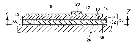
One embodiment of the RFID tag 30 of the present invention is illustrated in
Figure 5. The RFID tag 30 is shown attached to an item with finite electrical
conductivity,
such as a conductive object 24. The conductive object 24 may be metallic,
nonmetallic
(e.g., carbon-fiber based composite), or liquid (e.g., an aqueous ionic
solution in a bottle),
or any combinations thereof. In one embodiment, the RFID tag 30 is attached to
the
conductive object 24 by a first layer of adhesive 38. However, the RFID tag 30
may be
attached to the conductive object 24 by any known means in the art of
attaching items to
objects. The first layer of adhesive 38 is useful for attaching the RFID tag
30 to objects,
such as airplane parts, tools, metal bins and racks, and other air, land and,
sea
transportation vehicle parts. In Figure 5, the second layer of adhesive 40 is
opposite from
the integrated circuit 20 and antenna 18 on the first maj or surface 14 of the
substrate 12.
However, in another embodiment, the integrated circuit 18 and antenna 20 could
be on the
second major surface 16 of the substrate 12 and in contact with the second
layer of
adhesive. The RFID tag 30 may also optionally include a liner (not shown) on
the first
layer of adhesive 38. Suitable liner materials include polyethylene and
silicon coated
papers. The RFID tag 30 includes the RFID tag 10, which is described in more
detail in
reference to Figure 1. The RFID tag 10 is attached to a first spacer layer 32,
preferably by
a second layer of adhesive 40. However, the RFID tag 10 may be attached to the
first
spacer layer 32 by any known means in the art of attaching item to objects.
The first
spacer layer 32 has a first major surface 34 and a second major surface 36
opposite the
CA 02607599 2007-11-06
WO 2006/124270 PCT/US2006/016796
-12-
first major surface 34. The second layer of adhesive 40 is in contact with the
second
major surface 16 of the substrate 12 of the RFID tag 10 and the first major
surface 34 of
the first spacer layer 32. The first layer of adhesive 38 is in contact with
the second major
surface 36 of the first spacer layer 32 and the surface of the conductive
object 24.
The first spacer layer 32 is a composite layer, which includes microstructured
particles dispersed in a binder. Preferably, the binder is a nonmagnetic,
nonconductive
binder and the microstructured particles are multilayered flakes. However, the
microstructured particles may be of any shape or form.
Preferably, the composite layer 32 includes a thickness between 0.5 and 5.0
mm.
More preferably, the composite layer 32 includes a thickness between 0.5 and
2.
However, the composite layer 32 may be any thickness suitable for its intended
purpose.
Preferably, the areal density of the composite layer 32 is between 0.0001 and
0.1 gm/mm2.
More preferably, the areal density is between 0.0005 and 0.05 gm/mm2. However,
the
composite layer may be any areal density suitable for its intended purpose.
One example of a preferred binder is polyethylene and its copolymers.
Alternatively, a variety of polymers or polymer blends such as thermoplastic
polymers,
thermoplastic elastomers, and thermally activated or accelerated cure polymers
may be
used as binder material. The binder may also be a polymeric or nonpolymeric
adhesive.
In some embodiments, the RFID tag 30 may not require additional layers of
adhesive 38
and 40. Instead, the RFID tag 30 may only include the RFID tag 10 described in
reference
to Figure 1 and a layer of adhesive with the microstructured particles or
multilayered
flakes dispersed in the layer of adhesive.
The multilayered flakes each comprise at least one layer pair, each layer pair
comprising one thin film crystalline ferromagnetic metal layer adjacent to one
thin film
dielectric layer. In the case of flakes having two or more layer pairs, the
layer pairs form a
stack of alternating ferromagnetic metal layers and dielectric layers.
Typically, a
dielectric layer comprises both of the outermost layers of the stack. The
flakes are
randomly dispersed in the binder, although the flakes are preferably oriented
so that the
plane of the thin film layers is substantially parallel to the plane 'of the
material.
The flakes have a maximum major dimension in the plane of the thin film
layers,
which is preferably in the range from about 25 to about 6000 m. The flake
sizes of a
CA 02607599 2007-11-06
WO 2006/124270 PCT/US2006/016796
-13-
plurality of flakes generally occur in a distribution extending from the
maximum major
dimension to substantially zero. The size distribution of the flakes may be
altered by the
process used to disperse them in the binder. The thickness of the flakes,
i.e., the
dimension perpendicular to the plane of the thin film layers, may be chosen to
suit a
particular application. The ratio of the flake thickness to the maximum major
dimension is
typically from 1:6 to 1:1000, indicating a flalce that is relatively plate-
like in shape. This
ratio allows a magnetic field oriented in the plane of the flakes to penetrate
the
ferromagnetic metal layers readily with minimal depolarization.
The number of layer pairs in each flake is preferably at least 2, and more
preferably in the range from 2 to about 100. Flakes having from 10 to 75 layer
pairs are
more preferred.
The ferromagnetic metal layers comprise a crystalline ferromagnetic metal
alloy
having an intrinsic direct current (DC) perineability of at least 100 relative
to free space,
Amorphous alloys can be used for this invention but are less desirable because
of their
greater cost to obtain and process. The alloy preferably comprises NiFe
containing at most
80 % by weight Fe. The alloy may also include other magnetic or nonmagnetic
elements
such as Cr, Mo, Cu, and Co, as long as the alloy remains magnetic. Different
ferromagnetic metal layers in the same flake may comprise different alloys.
Dielectric layers 18 may be made of any known relatively non-conducting
dielectric material. Such materials include SiO, Si02, MgF2, and other
refractory
materials, and also may include polymeric materials such as polyimides. The
thickness of
each dielectric layer 18 is in the range from about 5 to about 100 nm.
The multilayered flakes are layers of two dissimilar materials. In one
preferred
embodiment, the layers of the multilayered flakes are Si02 and Ni(80):Fe(20)
(permalloy). In addition, the multilayered flalces are nonuniform throughout
their depth,
being alternating thin films of insulator (Si02) and magnetic metal
(permalloy). The
metals of the permalloy are metallic, i.e., in an unoxidized state (0
valence). The metals
are not chemically bonded to the Si02 nonmagnetic spacer layer. In contrast,
to the prior
art ferrite particles are chemically homogenous and physically uniform
throughout the
interior of the particle.
CA 02607599 2007-11-06
WO 2006/124270 PCT/US2006/016796
-14-
The flakes may be made by first depositing a stack of alternating
ferromagnetic
metal and dielectric layers of the desired materials on a substrate using a
known thin film
deposition technique, such as electron beam evaporation, thermal evaporation,
sputtering,
or plating. A preferred method uses electron beam evaporation in a
conventionally
designed vacuum system incorporating a vacuum compatible web drive assembly,
as
described in U.S. Pat. No. 5,083,112 (cols.4-5). The substrate may be, for
example, a
polyimide, a polyester, or a polyolefin, and is preferably in the form of a
flexible web. It is
believed that magnetically orienting the ferromagnetic metal layers during
deposition by
applying an aligning magnetic field to the growing films in the cross web
direction may be
beneficial for some applications.
After a stack is produced having the desired number of layers, the stack may
be
removed from the substrate. An effective method of removal includes passing
the
substrate around a bar with the stack facing away from the bar, the bar having
a
sufficiently small radius such that the stack delaminates from the substrate.
The stack may
shatter into flakes having a suitable size as the stack is delaminating.
Otherwise, the stack
is then broken into flakes having a desired maximum size by a method such as
grinding in
a hammer mill fitted with an appropriately sized screen. In another method for
making
flakes, the stack of alternating layers may be deposited on a substrate, which
is the same
as, or compatible with the binder to be used and the entire stack (including
the substrate) is
then broken into flakes.
To produce the finished composite, the flakes are then dispersed in the binder
using a suitable method such as blending. The mixture is thereafter formed
into a
configuration such as a tape, a sleeve, a sheet, a rope, pellets, or a
specifically configured
part by a method such as extrusion, pressing or molding. The configuration may
be
chosen to suit a particular application.
The quantity of flakes dispersed in the composite is preferably about 0.1 to
10 %
by volume, and more preferably about 0.3 to 5 % by volume.
Efficient coupling of magnetic field energy to the multilayered flalces of the
composite layer 32 is achieved when the thickness of the ferromagnetic layer
component
of the multilayered flakes is less than the skin depth of the electromagnetic
field coupling
into the layer. The full thickness of each ferromagnetic layer component
contributes to the
interaction with the magnetic field. The magnetic field is concentrated into
the composite
CA 02607599 2007-11-06
WO 2006/124270 PCT/US2006/016796
-15-
layer and the interaction of the magnetic field with the conductive object is
thereby
reduced.
If the particles or flakes are randomly dispersed, the macroscopic average of
the
relative magnetic permeability s of the spacer layer 32 is the spatial and
orientation
average of the several components of the microscopic relative magnetic
penneability
tensor ;jk of the microstructured particles, taken together with the relative
magnetic
permeability of the binder b. If the microstructured particles or
multilayered flakes are
oriented or aligned in the binder, then the relative magnetic permeability of
the composite
layer 32 may be better represented by a weighted average, with weighting
factors
accounting for the degree of order in the composite layer 32. For the purpose
of the
following discussion, assume a random dispersion so that the relative magnetic
permeability of the microstructured particles is represented by a scalar
number, and this
taken together with the magnetic permeability b of the binder will combine to
give a
macroscopic relative magnetic permeability of the spacer layer ( S). In this
case, the
energy in the magnetic field in the presence of the composite layer may be
expressed as
the volume integral of the product H B:
Magnetic field energy E=%Z J H=B dV =%Z J SHa dV
The magnetic field energy E is increased in the composite layer 32 in
comparison
to the magnetic energy in a similarly dimensioned nonmagnetic spacer, such as
Fome-
CorTM material included in the Examples, by a factor that is equal to the
average relative
magnetic permeability s. The net effect of the magnetically permeable
composite layer is
to confine the magnetic field energy and reduce the amount of energy coupled
to the
conductive substrate. This results in reduced eddy current induction in the
conductive
surface, resulting in turn in higher signal returned to the RFID reader.
One example of suitable composite layer 32 is taught in U.S. Pat. 5,925,455,
"Electromagentic-Power-Absorbing Composite Comprising a Crystalline
Ferromagnetic
Layer and a Dielectic Layer, Each Having a Specified Thiclcness," (Bruzzone et
al.),
which is hereby incorporated by reference. Although the Bruzzone et al.
reference teaches
that their composite layer is power-absorbing and used for applications to
bond two
objects together by heating the composite using electromagnetic power and
bonding the
CA 02607599 2007-11-06
WO 2006/124270 PCT/US2006/016796
-16-
two objects together by means of melting, fusing or adhesive curing, the
inventor of the
present invention has discovered new, unexpected properties affiliated with
the composite
disclosed in the reference. Specifically, the inventor discovered that for
some frequencies
reserved for radio frequency identification, such as 125 kHz and 13.56 MHz,
the
composite layer does not operate as a power-absorbing material. Instead, the
composite
later acts as a magnetic shield material for RFID applications where an RFID
tag is on a
conductive object, such as a metal object, thus allowing the RFID tag to be
successfully
read by an RFID reader. In addition, the inventor discovered that the magnetic
filed is
preferentially concentrated in the composite layer. With reduced magnetic
field in the
conductive substrate, Eddy currents are not included in the conductive
substrate, and the
RFID reader sees a higher returned signal from the RFID tag, enabling a
successful read of
the RFID tag by the RFID reader.
As illustrated in Figure 6, the RFID tag 30 may optionally include a cover
layer 50.
The cover layer 50 may be directly attached to the substrate 12 and/or antenna
18, for
example, by lamination. Alternatively, the cover layer 50 may be attached to
the substrate
12 and/or antenna 18 by a third layer of adhesive 48, as illustrated in Figure
6. The cover
layer 50 and third layer of adhesive 48 may be useful for attaching the RFID
tag 30 to a
conductive object 24. The cover layer 50 may extend beyond the substrate 12,
for
example, it might be a tape that is used to affix the RFID tag 30 to an
object. Suitable
materials for the cover layer 50 include polyester films or papers.
Alternatively, the cover
layer 50 and layer of adhesive 48 may be commercially available tape sold by
3M
Company, based in St. Paul. The cover layer 50 may be printed or patterned
with
information, for example, a company logo, an advertisement, or information
about the
object 24 to which the tag 30 is attached. The printed information may
specifically
include a bar code or other symbolic representation to allow a visual or
optical
confirmation of the information pertaining to the RFID tag 30. The cover layer
may be
stapled or otherwise attached to any item. The cover layer may be wrapped
around a
handle of luggage, for example, and then attached to itself to attach the RFID
tag to the
luggage.
In another alternative embodiment, the RFID tag 30 may include multiple
composite layers. As illustrated in Figure 6, the RFID tag may include a
second
composite layer 42, in addition to the first composite layer 32. However, the
RFID tag 30
CA 02607599 2007-11-06
WO 2006/124270 PCT/US2006/016796
-17-
may include any number of composite layers. The second composite layer 42
could be the
same or different from the first composite layer 32, which is described above.
For
example, the second composite layer 42 may include a different distribution or
quantity of
multilayered flakes, or a different binder material. The second composite
layer 42
includes a first major surface 44 and a second major surface 46 opposite the
first major
surface. The first composite layer 32 is attached to the second composite
layer 42 by the
first layer of adhesive 38. The first layer of adhesive is in contact with the
second major
surface of the first spacer layer 32 and the first major surface 44 of the
second composite
layer 42. The second composite layer 42 is attached to the conductive object
24 by a
fourth layer of adhesive 52. The second major surface 46 of the second
composite layer
42 is in contact with the fourth layer of adhesive 52.
Suitable adhesives for the layers of adhesives 38, 40, 48, 52 include a wide
range
of adhesives known to those skilled in the art, including, for example, those
based on
natural rubber, acrylate polymers, block copolymers, polyolefins and
polyolefin
copolymers. Pressure-sensitive adhesives may be preferred in some
applications.
Figures 7, 8, and 9 illustrate alternative embodiments of the RFID tag 30 of
the
present invention. In particular, Figures 7, 8, and 9 illustrate different
configurations of
the composite spacer layer 32. In Figure 7, the spacer layer 32 includes a
first portion 70
that includes the multilayered flakes 82. The spacer layer 32 also includes an
aperture or
hole 72. The first portion 70 and the aperture 72 is arranged such that the
multilayered
flakes 82 in the spacer layer 32 corresponds generally to the shape of the
antenna 18.
In Figure 8, the spacer layer 32 includes a first portion 74 and a second
portion 76.
In the first portion, the binder includes the multilayered flakes 82. In the
second portion
76, the binder does not include the multilayered flakes 82. Similar to the
embodiment
illustrated in Figure 7, the position of the multilayered flakes 82 correspond
generally to
the shape of the antenna 18.
In Figure 9, the spacer layer 32 includes a first portion 78 and a second
portion 80.
Both the first and second portions 78, 80 include multilayer flakes 82. The
first portion 78
and second portion 80 are arranged to correspond generally to only portions of
the shape
of the antenna 18. In this embodiment the first portion 78 and second portion
80 are two
individual strips attached to the second major surface 16 of the substrate 12.
CA 02607599 2007-11-06
WO 2006/124270 PCT/US2006/016796
-18-
It is advantageous to provide a composite spacer layer 32 where on average,
the
plane of the multilayered flalces 82 are aligned with the plane of the RFID
antenna 18 to
minimize demagnetization effects. Further, in these embodiments, less of the
composite
material or multilayered flakes is required, making the RFID tag less costly.
Figures 7, 8,
and 9 illustrate just three possible configurations of the composite spacer
layer 32.
However, any number of configurations or designs are contemplated so as to
provide a
spacer layer 32 where the spacer layer has some portion having multilayered
particles 82
and where this portion is aligned with at least one portion of the RFID
antenna 18.
The operation of the present invention will be further described witli regard
to the
following detailed examples. These examples are offered to further illustrate
the various
specific and preferred embodiments and techniques. It should be understood,
however,
that many variations and modifications may be made while remaining within the
scope of
the present invention.
For all of the exainples below, the RFID transponders used were Texas
Instruments
(TI), Inc. radio frequency identification Tag-ItTM HF-I ISO-15693
(International Standards
Organization) compliant transponder inlays with a 48 millimeter by 48
millimeter antenna
available from Texas Instruments, Inc., Dallas, TX. The RFID reader used to
read the
RFID transponders in all of the examples was a TEK Protege-TungstenTM handheld
reader
adapter from TEK Industries, Inc., Vernon, CT. The TEK Protege-TungstenTM
handheld
reader adapter from TEK Industries, Inc., was attached per the design
selection of TEK
Industries to a PalmOneTM Tungsten C personal digital assistant (PDA)
available from
PalmOneTM, Milpitas, CA.
To establish the readability of the TI transponders by the TEK Protege-
TungstenTM
handheld reader adapter attached to a PalmOneTM Tungsten C PDA, the TI
transponders
were read in free space, i.e., the transponders were not attached to metal,
nor were they
attached to any other RF absorbers. Using the TEK Protege-TungstenTM handheld
reader
adapter attached to a PalmOneTM Tungsten C PDA, hereinafter referred to as the
TEK
RFID reader, the TI transponders were read at a distance of up to 112
millimeters
measured from the RFID reader.
Then, the TI transponders were mounted directly on an aluminum plate, i.e. no
set
off distance between the TI transponder and the aluminum plate, nor was there
any other
CA 02607599 2007-11-06
WO 2006/124270 PCT/US2006/016796
-19-
RF absorbers placed between the TI transponder and the aluminum plate, and the
TI
transponders were not readable using the TEK RFID reader.
Comparatiye Example 1
For this comparative example, a polystyrene display board was used as a set
off
spacer layer between the TI transponder and an aluminum plate to provide
distance
between the TI transponder and the aluminum plate, but yet provide a
configuration in
which the TI transponder was affixed to the aluminum plate. The transponder
was affixed
to the display board and the display board in turn was affixed to the aluminum
plate as
follows. 3MTM double-sided adhesive tape available from 3M Company, St. Paul,
MN,
was laminated to the side of the TI transponder opposite the side upon which
the RFID
integrated circuit was affixed. The TI transponder with the double sided
adhesive tape
was then adhered by the tape to a 55 millimeter by 55 millimeter piece of Fome-
Cor
polystyrene display board 5.08 millimeters thick available from Alcan
Composities USA
Inc., St. Louis, MO. The mass of this piece of display board was 1.79 grams.
The display
board with attached transponder was then attached to an aluminum plate using
3MTM
double-sided adhesive tape laminated to the side of the display board opposite
the side to
which the transponder had been attached. Using the TEK RFID reader, the
transponder
was read at a distance of up to 53 millimeters measured from the RFID reader.
Comparative Example 2
In this comparative example, all elements were the same as in Comparative
Example 1 except that the polystyrene display board used as a spacer layer was
2.413
millimeters thick, and thus had a mass of 0.86 grams. Using the TEK RFID
reader, the
transponder was read at a distance of up to 39 millimeters measured from the
RFID reader.
Comparative Example 3
In this comparative example, the spacer layer was a 0.991 millimeter thick
layer of
iron filled silicone polymer magnetic absorber available under the tradename
of EccosorbTM
GDS material from Emerson & Cuming, Randolph, Ma. The length and width of the
magnetic absorber layer was 51 millimeters by 51 millimeters and had a mass of
6.89
grams. The transponder and the attachment method of transponder to the
magnetic
CA 02607599 2007-11-06
WO 2006/124270 PCT/US2006/016796
-20-
absorber and then to an aluminum plate were the same as described in
Comparative
Example 1. Using the TEK RFID reader, the transponder was read at a distance
of up to
39 millimeters measured from the RFID reader.
Example 4
In this example, a composite layer of the present invention was used as the
spacer
layer. The micro structured particle composite layer used as the spacer layer
in this
example was formed from two thinner sheets of the composite film laminated
together
with 3MTM Post-ITTM double-sided adhesive tape. The resultant spacer layer was
55
millimeters by 55 millimeters with a total thickness (two film layers and an
interlayer tape
layer) of 0.813 millimeters and a mass of 2.49 grams. The transponder was
attached to the
composite film spacer layer and the combination of the composite film spacer
layer and
transponder were in turn attached to the aluminum plate as set forth in
Comparative
Example 1. Using the TEK RFID reader, the transponder was read at a distance
of up to
40 millimeters measured from the RFID reader.
Comparative Example 5
In this comparative example, all elements were the same as in Comparative
Example 1 except that the spacer layer was composed of 8 sheets of plain white
20-pound
paper. The plain paper spacer layer comprised of 8 sheets of paper had a
thickness of
0.813 millimeters and the length and width dimensions were cut to 55
millimeters by 55
millimeters. The resultant paper spacer layer had a mass of 1.98 grams. Using
the TEK
RFID reader, the transponder was read at a distance of up to 20 millimeters
measured from
the RFID reader.
The results of the transponder read ranges relative to the type of spacer
layer used
over a metal surface in each of the above examples is set forth in the
following Table.
CA 02607599 2007-11-06
WO 2006/124270 PCT/US2006/016796
-21-
Length Read
Spacer Width Areal Range
Example Layer Dimensions Thickness Mass Density on
No. Construction (mm) (mm) (gr.) (gm/mm) Metal
(MM)
Cl Fome-CorTM material 55 x 55 5.080 1.79 0.59x10 53
3
39
C2 Fome-CorTM material 55 x 55 2.413 0.86 0.28x10"
C3 EccosorbTM GDS 51 x 51 0.991 6.89 0-3 39
material
composite layer of the
present invention
4 55 x 55 0.813 2.49 0.82x10"3 40
C5 Paper 55 x 55 0.813 1.98 0.65 1 0- 20
As denoted by the results presented in the above table, RFID transponders
mounted
on a composite layer of the present invention and affixed to a conductive
surface were
readable at a comparable read range to RFID transponders mounted on prior art
shield
layer materials, such as EccosorbTM material, that was also affixed to a
conductive surface.
The composite layer of the present invention included a comparable thickness,
but
approximately one third the mass, compared to the EccosorbTM material.
Further, RFID
transponders mounted on a composite layer of the present invention and affixed
to a
conductive surface provided a comparable read range to an RFID transponder
mounted on
spacer layer materials, such as Fome-CorTM material that was also affixed to a
conductive
surface. The composite layer of the present invention included a slightly
higher mass, but
a significantly lower thickness, compared to the Fome-CorTM material.
The tests and test results described above are intended solely to be
illustrative,
rather than predictive, and variations in the testing procedure can be
expected to yield
different results.
The present invention has now been described with reference to several
embodiments thereof. The foregoing detailed description and examples have been
given
for clarity of understanding only. No unnecessary limitations are to be
understood
therefrom. All patents and patent applications cited herein are hereby
incorporated by
reference. It will be apparent to those skilled in the art that many changes
can be made in
the embodiments described without departing from the scope of the invention.
Thus, the
CA 02607599 2007-11-06
WO 2006/124270 PCT/US2006/016796
-22-
scope of the present invention should not be limited to the exact details and
structures
described herein, but rather by the structures described by the language of
the claims, and
the equivalents of those structures.