Note : Les descriptions sont présentées dans la langue officielle dans laquelle elles ont été soumises.
CA 02608025 2007-11-09
WO 2005/112042 PCT/GB2005/001767
1
OPTOELECTRONIC TWEEZERS
The present invention relates to a micro-fluidic device including integrally
formed
semi-conductor lasers. In particular, the invention relates to a device that
is operable
to form optical tweezers or provide counter propagating beam optical trapping
and
further optical guiding within a micro-fluidic channel.
Optical tweezers allow micrometer-sized particles to be held, moved and
generally
manipulated without any physical contact. This has been well documented, see
for
example Ashkin et al Optics Letters Vol. 11, p288 (1986). Tweezers work
primarily
upon refraction of light (when considering particles bigger than the
wavelength). Due
to this attractive property, they have found many uses, especially in
biomedical
research where they enable the manipulation and separation of cells, DNA,
chromosomes, colloidal particles etc.
The operation of optical tweezers relies on the gradient force. This is the
force that
particles experience in the presence of a laser beam. To use optical tweezing,
particles
are typically suspended in solution. A laser beam is directed onto the
specimen via a
microscope, which enables control over its beam properties, such as shape,
size and
number of focal spot(s), as well as depth of field. By varying the properties
of the
beam, particles within its range can be manipulated.
As an alternative to optical tweezing, an optical trap can be formed using two
counter
propagating diverging beams due to a combination of optical refraction and
optical
scattering. An example of this counter-propagating arrangement is described in
the
article "Demonstration of a Fibre-Optical Light-Force Trap" by Constable et
al., Opt.
Lett. 1992. This uses two optical fibres that deliver light to a trap region
in a counter-
propagating geometry. Other articles describing particle manipulation in this
geometry
include "The Optical Stretcher: A Novel Laser Tool to Micro-manipulate Cells"
by
Guck et el, Biophysical Journal, Vol 81, August 2001, and "Micro-instrument
Gradient Force Optical Trap" by Collins et al, Applied Optics, Vol 38, No 28/
1 Oct
1999.
SUBSTITUTE SHEET (RULE 26)
CA 02608025 2007-11-09
WO 2005/112042 PCT/GB2005/001767
2
Although optical tweezers and other traps using light, such as the counter
propagating
beam trap, have proven themselves as a general interdisciplinary tool in
engineering,
physics and biology, serious drawbacks prevent them from fully realising their
potential. In the case of optical tweezing, this is primarily because of the
conventional
approach to the tweezing geometry, which uses a microscope objective lens and
a
standard Gaussian laser beam. This arrangement can only provide a single
ellipsoidal
trap, elongated along the optic axis. Furthermore, the size and the related
cost and
complexity of conventional microscopy limit the range of applications for
which
optical tweezing can be used. A yet further problem is that conventional
techniques
offer little flexibility for tailoring the optical potential in 3-D space, and
dynamic
multiple trapping can only be realized by time-multiplexing single traps.
Similar
problems exist for the counter propagating beam trap, i.e. the need for
external
(bulk)optics and lasers either propagating in free space or delivered through
a fibre,
and issues due to time multiplexing.
An object of the present invention is to overcome at least in part some of the
problems
known with both optical tweezing and counter-propagating beam trap
arrangements.
According to the present invention, there is provided a micro-fluidic device
fabricated
using semiconductor material, the device having a micro-fluidic channel or
chamber
defined within the material and one or more semiconductor lasers that are
operable to
form an optical trap, or a partial trap, in the channel or chamber. By partial
trap it is
meant that the lasers may be operable to define a perturbation in the optical
field that
is sufficient to deflect or guide a particle, but not necessarily hold that
particle.
By defining one or more lasers in the material that forms the channel itself,
an optical
trap can be created without the need for a microscope system to deliver light
into the
chamber. Instead, tweezing and/or trapping can be done using the in situ
lasers that are
already pre-aligned and thus create a truly integrated optical trap.
The optical trap may be formed by using counter-propagating beams derived from
one
or more lasers. Additionally or alternatively, one laser may be used to
produce a
shaped beam that is operable for use as an optical tweezer. Here an output
lens may
be used for trapping. Particle guiding may also be performed using such a
system.
SUBSTITUTE SHEET (RULE 26)
CA 02608025 2011-06-30
3
Preferably, electrical connections are provided on the device and the
semiconductor
material is an electro-luminescent material. In this way, the output of the
laser(s) can
be carefully controlled, thereby providing a mechanism for manipulating the
output
beam and so move or manipulate a particle.
Detecting means for detecting the presence of a particle in the trap may be
provided.
This might take the form of observation via a microscope or could be imaging
of
scattered light onto a photodiode.
Preferably, the walls of the lasers are coated with an electrically insulating
material.
The electrically insulating material may be optically transparent or operable
to have an
optical effect on light emitted from the lasers. For example, the coating
material could
be chosen to provide beam-shaping functionality e.g. by patterning the coating
material and/or varying its thickness across the facet.
Banks of optical traps may be provided next to one another to allow shunting
of a
particle between one trap and another. Shunting may be performed by suitable
control
of the microfluidic flow or by use of an integrated laser for pushing. In this
manner
the trapped object may be multiply interrogated in these traps. Tasks that may
be
performed in each trap region may include optical stretching, spectroscopy
(e.g.
Raman), and photoporation. Trapping is not restricted to colloidal trapping
but
encompasses biological particles such as cells, chromosomes and bacteria.
According to an aspect of the present invention there is provided an on-chip
monolithic micro-fluidic device fabricated using a semiconductor material, the
device having a micro-fluidic channel or chamber defined within the
semiconductor
material and one or more monolithically integrated semiconductor lasers
defined in
the semiconductor material that forms the channel, the one or more
semiconductor
lasers being operable to form at least one optical trap or partial optical
trap in the
channel or chamber.
Various aspects of the invention will now be described with reference to the
accompanying drawings, of which:
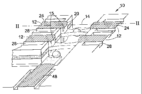
Figure 1 is a perspective view of a micro-fluidic device that has a channel
that
is defined by a plurality of semiconductor lasers;
Figure 2 is a section on line 1I-II of Figure 1;
CA 02608025 2011-06-30
3a
Figure 3 is a plan view of a micro-fluidic device with integral fluid
reservoirs,
and
Figure 4 is a view of a particle trapped in the channel between two integrated
lasers of the devices of Figures 1 and 3.
CA 02608025 2007-11-09
WO 2005/112042 PCT/GB2005/001767
4
Figures 1 and 2 show a micro-fluidic device 10 formed from a semiconductor
material. This device 10 has two pairs of monolithically integrated
semiconductor
lasers 12 integrally formed from the semiconductor material. Each pair of
lasers
comprises two identical semiconductor lasers 12 positioned directly opposite
each
other on opposing sides of a micro-fluidic channel 14, which is defined, at
least partly,
by the ends of the lasers 12. The channel 14 is provided for receiving fluid
that
includes the particles of interest. The channel depth depends upon the size of
particle
to be studied, and can vary from 2 m to about 50 m.
Each laser 12 is made from a semiconductor material that comprises an active
layer
16, typically consisting of multiple quantum wells, such as layers of GaAs, or
quantum wells, sandwiched between two cladding layers 18, for example GaAs,
which provide optical confinement. The lasers 12 are defined firstly by
etching a
series of ridges 20. As will be appreciated by a skilled person, to ensure
transverse
optical confinement is achieved, the regions between the ridges 20 have to be
etched
far enough down to generate the effective index contrast required for guiding.
As an
example, for an active layer that is 800nm beneath the surface of the
material,
typically the material would be etched to 500-600nm from the surface, leaving
300-
200nm above the active layer. Defining the ridges can be done using any
suitable
etching process, for example reactive ion etching or chemically assisted ion
beam
etching. To prevent optical and electrical coupling of neighbouring lasers,
the ridges
must be spaced by at least 30 m, unless isolation trenches are added.
To define the length of the lasers, facets that provide feedback are formed at
the ends
of the ridges 20. To form the facets 15 that face one another across the
channel 14,
the semiconductor material is etched to a depth of at least twice that of the
active
layer. A deeper channel can be etched between opposing facets 15 to
accommodate
larger particles, if necessary. The facets at the other ends of the lasers
(not shown) are
formed either by etching or by cleaving the material.
On an upper surface of each laser 12 is an electrical contact 24 for allowing
electrical
pulses to be applied to the laser material to stimulate the production of
laser radiation.
The upper contact 24 can be made from any suitable conductive material forming
an
Ohmic contact to the semiconductor, for example a 20nm layer of nickel on the
GaAs
SUBSTITUTE SHEET (RULE 26)
CA 02608025 2007-11-09
WO 2005/112042 PCT/GB2005/001767
with a 200nm layer of gold on top. On a back surface of the device, a back
contact
(not shown) is provided. Although not shown in Figures 1 or 2, in order to
ensure that
current passes only through the lasers, the regions between the ridges are
typically in-
filled with an insulating material, such as SU8 polymer.
Because the device of Figure 1 is designed to investigate particles suspended
in fluids,
it is necessary to take steps to avoid electrical short circuits between the
various layers
of the lasers 12. To do this, an electrically insulating material is applied
to the interior
walls that define the channel. This can be done using UV lithography. The
resist used
can be of any suitable type, for example SU-8 polymer. Exposure to UV
radiation
cures the SU-8. Uncured regions are washed away in a solvent. Doing this
allows the
bottom of the channel 14 can be coated, for example to a depth of about 300nm.
A
thicker SU-8 blend is then patterned using UV to cover the etched facets 15 of
the
lasers 12, the walls of the deeply-etched channel 14, and the ends of the
electrical
contacts 24. This reduces the width of the channel by a few microns on each
side, and
increases the divergence of the beam by a few degrees. Figure 2 shows a
section
through a single pair of lasers 12 having end faces and upper contacts that
are coated
in SU-8. In order to allow electrical connection to the lasers, the ends of
the upper
contacts that are remote from the channel 14 are exposed so that contact can
be made
thereto.
Figure 3 shows an illustration of a possible arrangement for facilitating the
supply of
fluid to the micro-fluidic channel =14. In this, a trapping device 34 is
mounted on a
larger micro-fluidic chip 36. On the chip 36, there is provided a fluid supply
chamber
or reservoir 38 that has a fluid input port 40 for allowing fluid to be
introduced into
the chamber 38. Opposite this is another chamber 42 that has a fluid output
port 44.
This can be fabricated by UV lithography in a thick layer of SU-8, or by
embossing a
polymer such as PDMS, or from glass panels held in place by a suitable
sealant. At an
output port of the input chamber 38 is a pump 46 for causing a fluid flow from
that
chamber into the micro-fluidic channel 14 of the trapping device 34. This pump
46
could be an external mechanical or gravity-fed pump; or it could be an on-chip
micro-
pump, such as an electro-osmotic pump, or some form of MEMS actuator. In this
way, fluid can be pumped from the input reservoir 38 into the trapping device
channel
14 and from there into the output reservoir 42 in a controllable manner.
Further
SUBSTITUTE SHEET (RULE 26)
CA 02608025 2007-11-09
WO 2005/112042 PCT/GB2005/001767
6
control could be exercised by using a plurality of the lasers to guide
particles through
the channel 14. This can be done by individually and sequentially addressing
the
lasers. Alternatively or additionally, a guiding laser 48 may be provided for
projecting light along the longitudinal axis of the channel 14, thereby to
push or guide
particles along the channel length, as shown in Figure 1.
Although not shown in Figure 3, in practice a lid is necessary to prevent both
contamination and evaporation of the sample, and to allow for pumping through
the
device. A simple lid can be a piece of glass or a membrane of PDMS mounted on
top,
or a layer of oil. But a preferred solution is to create the lid from the same
material
that constitutes the chamber 38 and 42. In the case of SU-8, a lid can be
formed by
using a lower exposure dose in the lid region so that only upper parts are
cross-linked,
whilst deeper parts remain unexposed, therefore soluble and can be removed
subsequently. Alternatively, the chamber and lid could be moulded from a
single
piece of polymer such as PDMS, or from glass panels held together with
sealant, such
as wax or exopy. Whilst evaporation from the input and output ports 40 and 44
is
likely to be minimal, valves could be incorporated to eliminate it completely.
The lasers of Figures 1 to 3 may be designed to give up to 20mW of output
power
(CW), in a single transverse mode. The emission peak is centred around 980nm
for
quantum wells and 1290nm for quantum dots, and is generated by injecting an
electrical current into the quantum well or quantum dot structures. The single
transverse mode measures about 1 m high and about 10 m wide within the
material.
As it leaves the material, it diverges at roughly 10 horizontally, and about
50
vertically, although these properties are subject to the specific
heterostructure design
and can be adjusted. It should be noted that a degree of beam divergence is
necessary
for optical trapping.
In use of the devices of Figure 1 to 3, electrical pulses are applied to the
contacts of
one pair of lasers 12. This generates two counter-propagating light beams,
which
interact to form a trap for manipulating or moving a particle 30, as shown in
Figure 4.
The specific design and output of the lasers 12 required to form a suitable
trap depend
on various parameters, and in particular the size of the particles that are to
be moved
or manipulated. As an example, GaAs/AlGAs quantum well lasers of length Imm
SUBSTITUTE SHEET (RULE 26)
CA 02608025 2011-06-30
7
have a threshold current of 20mA, and give 8mW of output power for an injected
current of 100mA. This is sufficient to deflect and trap particles of a few
microns in
size, and to produce bright scattering. The size of the trapping force is
determined
partly by the separation of the lasers, as defined by the channel's width,
which is
typically 20-50 m, and the optical power output.
Because semi-conductor processing techniques are well established and can be
used to
make small features, the device in which the invention is embodied opens up
the
opportunity for optical tweezing to be used outside a lab environment. Also,
it makes
available many options for shaping the lasers so that the output beam can be
tailored
for specific applications. In particular, lithographic fabrication processes
offer the
option of controlling the shape of the output beam in the horizontal plane,
e.g. by
forming lenses or holographic optical elements at the laser output facets 15.
The beam
can thereby be tailored to suit different tweezing and other optical
functions. Shaping
the beam in the vertical direction is possible by exploiting different
material
properties; these could be a graded GaAs/AlGaAs alloy cladding, for example.
By
applying a wet etching process that is sensitive to the alloy composition, a
lens-shaped
cross-section could be formed. It might also be possible to create lenses in
the SU-8
polymer that insulates the facets, either by lithographic means or by dry-
etching.
The device in which the invention is embodied can be used for many different
optical
tweezing or trapping applications. For example, for fluorescence applications,
the
laser material can be chosen to have wavelength that matches the sample's
absorption
peak. In this case, detection can make use of the same material, so long as
the
sample's fluorescence falls within the material's absorption peak. This is
advantageous.