Note : Les descriptions sont présentées dans la langue officielle dans laquelle elles ont été soumises.
CA 02611844 2011-07-04
1
WIDE RANGE POWER SUPPLY
BACKGROUND OF "TIF INVENTION
100011 The present invention is related to power supply systems, and more
specifically to
wide range power supply devices.
[00021 Such devices are used, for example, in protein electrophoresis,
isoelectric
focusing, DNA sequencing, and electrophoretic blotting.
[0003] Protein electrophoresis and isoelectric focusing demand power supplies
that meet
diverse requirements of delivering voltages from less than 20V to several
kilovolts. Thus, these
power supplies may be termed wide range power supplies. These power supplies
also need to be
efficient and able to perform in different modes such as the constant voltage,
constant current,
constant power, timed modes, and constant volt hour modes.
100041 Current power supply configurations are impractical for achieving
voltages as
high as 5000V and do not provide high precision in the output voltage. For
example, power
supplies that use a flyback transformer require multiple windings whose
outputs are rectified and
connected in series to achieve high voltages. The many windings required for
such high voltages
create a bulky and expensive power supply. A flyback configuration, as well as
other switching
power supplies, also suffer from high electromagnetic interference (NMI) as
follows.
100051 For reasons of efficiency, size weight and cost, switch mode power
conversion is
a standard design. Switching power supplies generate EMI as a result of
electric currents being
switched at high frequencies. Regulatory requirements demand that this noise
level be below
certain prescribed guidelines to ensure that electronic equipment does not
affect operation of
other equipment in the vicinity. The magnitude of this EMI generated depends
on the switching
mechanism employed.
CA 02611844 2007-12-11
WO 2007/008585 PCT/US2006/026330
2
[0006] Hard-switched flyback converters have sharp rising and falling edges on
the voltage
waveforms and pulsating current waveforms, which generate relatively higher
EMI. Thus,
increased filtering is needed, which results in a higher cost of the end
product. Also, the large
number of windings on a flyback transformer causes poor coupling of magnetic
flux between
the primary and the secondary windings. This results in a higher leakage flux,
which requires
the additional cost of higher radiated EMI filtering. Running at high power,
flyback
transformers also generate relatively higher common mode EMI, which reduces
efficiency of
the power conversion stage.
[0007] The precision of current power supply configurations is also limited by
the current
switching and regulation mechanisms. For example, in a conventional
architecture the power
converter control is prone to time and temperature drift. Additionally,
galvanic isolation of
input and output is a design need so as to meet product safety and regulatory
requirements,
and current feedback patterns within using isolation circuitry produce offset
errors and
non-linearities.
[0008] Therefore, it is desirable to provide methods, apparatus, and systems
for efficiently
supplying wide voltage ranges with high precision and reliability.
BRIEF SUMMARY OF THE INVENTION
[0009] Accordingly, embodiments of the present invention provide methods,
apparatus, and
systems capable of delivering from less than 20V to more than 5000V. A power
supply in
accordance with the embodiments of the present invention uses switch mode
technology to
achieve high overall operating efficiency and is capable of operating from no
load to full load
without loss of regulation. The power supply in accordance with the
embodiments of the
present invention operates directly from the utility supply (e.g., 110V/220V
and 50Hz/6OHz).
[0010] In one exemplary embodiment of the present invention, a wide range
power supply
device for protein electrophoresis, isoelectric focusing and electrophoretic
blotting is
provided. The power supply's power conversion stage includes: an input
rectifier; a do/dc
converter; a resonant inverter; and a voltage multiplier. The above indicated
stages are
connected in. series to achieve the large output voltage range. The power
supply includes a
power supply controller operatively coupled with the do/dc converter and the
resonant
inverter. The power supply controller is coupled with the output voltage via
one or more
feedback loops.
CA 02611844 2007-12-11
WO 2007/008585 PCT/US2006/026330
3
[0011] The do/dc converter may be a buck converter, a buck-boost converter, or
other
suitable do/dc converter. The resonant inverter may be a quasi-resonant
inverter, which can
have different designs, such as a half-bridge or an H-bridge. Also, other
inverters may be
used, such as resonant pole inverters, resonant do link inverter, or resonant
snubber inverters.
One embodiment of the present invention uses a transformer with single
secondary winding
and smooth waveforms due to resonant switching which generate relatively lower
EMI and
hence reduce the cost of EMI filter network employed. In another embodiment,
the voltage
multiplier also acts as a rectifier of a signal from the transformer.
[0012] In one embodiment, the wide range power supply device also includes a
supervisory
controller operatively coupled with the power supply controller. The coupling
is
accomplished with an optically isolated digital interface. The supervisory
controller may be
part of one of the feedback loops. In this embodiment, the supervisory
controller sends a
digital signal to the power supply controller. The digital signal may include
information as to
an error in the output voltage, and the information may include a new voltage
setting for the
power conversion stage.
[0013] In another embodiment, the wide range power supply device includes an
analog
optocoupler, where the analog optocoupler is part of an analog feedback loop
from the output
voltage to the power supply controller.
[0014] In another exemplary embodiment of the present invention, a method for
controlling
an output voltage of a switched-mode power supply is provided. A first set
point is received
at a power supply controller. A set point includes an output voltage setting.
The output
voltage is generated via control signals sent by the power supply controller
to a power
conversion stage. In one embodiment, the control signals are PWM signals. An
input of the
power conversion stage is galvanically isolated from the output voltage. The
output voltage
is measured with a supervisory controller.
[0015] An error in the output voltage is calculated with the supervisory
controller using the
output voltage and a reference voltage. A digital signal is transmitted from
the supervisory
controller to the power supply controller based on the error. The supervisory
controller is
galvanically isolated from the power supply controller. The control signals
are altered based
on the digital signal, which can achieve a higher precision voltage setting
for the power
supply. In one embodiment, the digital signal is transmitted through a digital
optocoupler,
CA 02611844 2007-12-11
WO 2007/008585 PCT/US2006/026330
4
where the digital optocoupler provides galvanic isolation between the power
supply
controller and supervisory controller.
[0016] In another embodiment, the method also includes transmitting, via an
analog signal,
the output voltage to the power supply controller, and using the analog signal
in a feedback
loop to alter the control signals to the power conversion stage. The digital
signal may include
a second set point, which includes a new voltage setting that compensates for
the error in the
output voltage from the desired voltage. The analog signal may be transmitted
through a
linear optocoupler, where the linear optocoupler provides galvanic isolation
between the
output of the power supply and the power supply controller.
[0017] In yet another embodiment, the method also includes receiving the first
set point at a
control board processor; sending the first set point to the supervisory
controller; and digitally
sending the first set point to the power supply controller.
[0018] In another exemplary embodiment of the present invention, a wide range
power
supply device is provided. This power supply has a power conversion stage, a
power supply
controller, and a supervisory controller. The power supply controller is
operatively coupled
with the power conversion stage, and is coupled with an output voltage of the
wide range
power supply via one or more feedback loops. The supervisory controller is
operatively
coupled with said control processor. The coupling is accomplished with an
optically isolated
digital interface, and the supervisory controller is part of one of the
feedback loops.
[0019] In one embodiment, the supervisory controller sends a digital signal to
the power
supply controller. The digital signal includes information as to an error in
the output voltage.
The information may include a new voltage setting for the power conversion
stage.
[0020] In yet another exemplary embodiment of the present invention, a power
supply in
accordance with embodiments of the present invention uses a fully digital
control
architecture. Control is achieved through a power supply controller, which may
be a digital
signal processor (DSP). The digital architecture enables the control to adapt
to the changing
load conditions. In a conventional architecture where the power converter
control is analog
and the supervisory functions are controlled by a microprocessor, the
converter control is
prone to time and temperature drift. The pure digital architecture makes the
control system
generally time and temperature invariant. In one embodiment, the control
architecture uses
three processors. The three processors use an optically isolated interface to
communicate
CA 02611844 2011-07-04
using a unique protocol for communication that enables reliable operation in a
noisy
environment such as a switching power supply.
[0020a] In accordance with another illustrative embodiment, a wide range power
supply
device for protein electrophoresis, isoelectric focusing and electrophoretic
blotting, includes a
5 power conversion stage. The power conversion stage has an input rectifier
connected with a
utility supply, a dc/dc converter connected with the input rectifier, a
resonant inverter connected
with the dc/dc converter, a transformer connected with the resonant inverter,
and a voltage
multiplier connected with the transformer and connected with an output voltage
of the wide
range power supply device. The device further includes a power supply
controller operatively
coupled with the dc/dc converter and the resonant inverter. The power supply
controller is
coupled with the output voltage via one or more feedback loops. The device
further includes a
supervisory controller operatively coupled with the power supply controller,
wherein the
coupling is accomplished with an optically isolated digital interface.
[0020b] In accordance with another illustrative embodiment, a method for
controlling an
output voltage of a switched-mode power supply includes receiving a first set
point at a power
supply controller, wherein the first set point includes an output voltage
setting. The method
further includes generating the output voltage via control signals sent by the
power supply
controller to a power conversion stage, wherein an input of the power
conversion stage is
galvanically isolated from the output voltage. The method further includes
measuring the output
voltage with a supervisory controller, and calculating, with the supervisory
controller, an error in
the output voltage using the output voltage and a reference voltage. The
method further includes
transmitting a digital signal from the supervisory controller to the power
supply controller based
on the error, wherein the supervisory controller is galvanically isolated from
the power supply
controller. The method further includes altering the control signals based on
the digital signal.
[0020c] In accordance with another illustrative embodiment, a wide range power
supply
device includes a power conversion stage, and a power supply controller
operatively coupled
with the power conversion stage. The power supply controller is coupled with
an output voltage
of the wide range power supply via one or more feedback loops. The device
further includes a
supervisory controller operatively coupled with the power supply controller.
The coupling is
accomplished with an optically isolated digital interface, and the supervisory
controller is part of
one of the feedback loops.
CA 02611844 2011-07-04
5A
[0021] The following detailed description together with the accompanying
drawings will
provide a better understanding of the nature and advantages of illustrative
embodiments of the
present invention.
BRIEF DESCRIPTION OF THE DRAWINGS
[0022] Fig. 1 is an exemplary simplified block diagram of a power supply in
accordance
with the embodiments of the present invention.
[0023] Fig. 2 shows a schematic of a switching circuit of a power supply in
accordance
with the embodiments of the present invention.
[0024] Fig. 3 shows a schematic of a voltage multiplier circuit of a power
supply in
accordance with the embodiments of the present invention.
[0025] Fig. 4 is an exemplary simplified block diagram of a power supply
utilizing a
digital feedback loop in accordance with the embodiments of the present
invention.
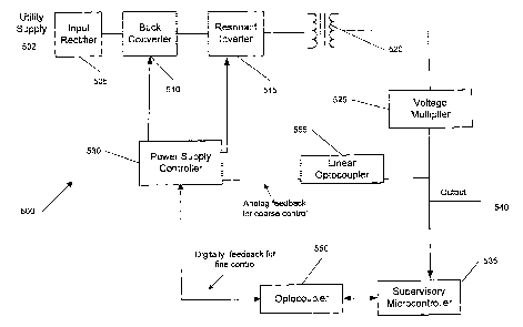
[0026] Fig. 5 is an exemplary simplified block diagram of a power supply
utilizing a
hybrid feedback loop in accordance with the embodiments of the present
invention.
[0027] Fig. 6 shows a method of running a power supply utilizing a hybrid
feedback loop
in accordance with the embodiments of the present invention.
[0028] Fig. 7 is an exemplary top-level block diagram of the power supply in
accordance
with the embodiments of the present invention.
[0029] Fig. 8 is a second-level block diagram of the power supply in
accordance with the
embodiments of the present invention.
[0030] Fig. 9 is a third-level block diagram corresponding to the block
diagram of Fig. 8,
showing a block diagram for the main board of Fig. 8.
[0031] Fig. 10 is a third-level block diagram corresponding to the block
diagram of Fig.
8, showing a block diagram for the control board of Fig. 8.
[0032] Fig. 11 is a third-level block diagram corresponding to the block
diagram of Fig.
8, showing a block diagram for the display board of Fig. 8.
CA 02611844 2007-12-11
WO 2007/008585 PCT/US2006/026330
6
DETAILED DESCRIPTION OF THE INVENTION
[0033] Embodiments of the present invention provide a wide range power supply
capable
of delivering 20V to 5000V. The power supply in accordance with the
embodiments of the
present invention uses switch mode technology to achieve high overall
operating efficiency
and is capable of operating from no load to full load without loss of
regulation. The power
supply may operate directly from the utility supply (e.g., 110V/220V and
50Hz160Hz).
[0034] Unless defined otherwise, all technical and scientific terms used
herein have the
meaning commonly understood by a person skilled in the art to which this
invention pertains.
As used herein, the following acronyms are defined as follows: constant
current (CC);
constant voltage (CV); constant power (CP); power factor correction (PFC);
analog to digital
converter (ADC); pulse width modulation (PWM); liquid crystal display (LCD);
resistor
capacitor series circuit (RC-circuit); inductor-capacitor (LC), digital signal
processor (DSP),
and electromagnetic interference (EMI).
[0035] Figure 1 shows an exemplary simplified block diagram 100 of a power
supply in
accordance with the embodiments of the present invention. As shown in Fig. 1,
the power
supply's power conversion stage includes the following elements an input
rectifier 105; a
buck converter 110; a resonant inverter 115; a transformer 120, and a voltage
multiplier 125.
These stages are connected in series to achieve the large output voltage
range. The operation
of the power supply is controlled by a power supply controller 130 to generate
the desired
output 140. Power supply controller 130 receives a feedback signal 145, which
may be
accomplished through optocouplers for isolation of the input and output of
power supply 100.
In one embodiment, power supply controller 130 is a digital signal processor
(DSP).
[0036] Input rectifier 105 rectifies an input utility supply AC voltage 102 to
an un-
regulated DC voltage. In one embodiment, the rectifier is a full wave
rectifier. In other
embodiments, a half-wave or other type of rectifier may be used. The rectifier
may also act
as a voltage doubler.
[0037] Buck converter 110 receives the un-regulated DC voltage from input
rectifier 105
and produces a variable DC voltage, e.g. from 1V to 195V. Depending on the
application,
other embodiments may utilize other DC/DC converters, such as a buck-boost
converter. If
low voltages are not desired, a boost converter may be used as well. The
output voltage of
CA 02611844 2007-12-11
WO 2007/008585 PCT/US2006/026330
7
the buck converter is regulated by power supply controller 130 in accordance
with preset,
values or dynamically based on output 140.
[0038] In one embodiment, power supply controller 130 controls buck converter
110 with
PWM signals, e.g. by regulating the duty cycle of the PWM signal. As the
output of rectifier
105 is unregulated, buck converter 110 allows a higher precision DC voltage to
be generated.
This higher precision DC voltage allows greater precision in the output 140.
In one
embodiment, the operating frequency of buck converter 110 may be changed to
improve the
precision of control. This improvement in precision may particularly be useful
for very light
loads.
[00391 Figure 2 shows a schematic of buck converter 110 according to an
embodiment of
the present invention. In Figure 2, two switches 205 and 210 are used in buck
converter 110.
In other embodiments, one switch or more than two switches may be used. The
switches may
be MOSFETs, such as IRFPE50 made by International Rectifier, or another
suitable
switching device. A free wheeling diode 215 is connected after the switches
and before a
series combination of an inductor 220 and output filter capacitor 225. In one
aspect, output
filter capacitor 225 has a capacitance of about 100uF (400V) and inductor 220
has an
inductance of about 2.5mH. In another aspect, the buck converter operates at
100kHz
switching frequency by alternately switching MOSFET's 205 and 210. These
stated values
for the components help to provide the desired range of voltage output by the
power supply.
[0040] Resonant inverter 115 receives the regulated DC voltage from buck
converter 110
and produces an alternating and relatively smooth waveform. The inverter may
be
quasi-resonant in that switching takes place at approximately zero current to
reduce EMI and
switching losses. In one embodiment, quasi-resonant inverter 115 is a variable
frequency
half bridge inverter configuration which is operated at a frequency above the
resonant
frequency. The frequency of resonance may be determined by the load impedance,
values of
an LC filter at the output of the inverter, and/or other passive components
connected at the
output of the inverter.
[0041] Figure 2 shows a schematic of resonant inverter 115 according to an
embodiment of
the present invention. In this embodiment, resonant inverter 115 is a half-
bridge
quasi-resonant inverter. In Figure 2, two switches 255 and 260 are used to
create an AC
signal. The switches may be MOSFETs, such as SPW47N6OC3 made by Infenion
Semiconductor, or other suitable switching device. In one aspect, resonant
inverter
CA 02611844 2007-12-11
WO 2007/008585 PCT/US2006/026330
8
capacitors 265 and 270 are about 0.047uF (1600V). Switch 255 and capacitor 265
are
connected with one side of output filter capacitor 225 of buck converter 110.
Switch 260 and
capacitor 270 are connected with the other side of output filter capacitor
225. Note that other
circuit elements may occur between buck converter 110 and resonant inverter
115 as well as
within themselves.
[0042] A line between the switches 255 and 260 is connected with one end of
the resonant
inverter output filter and another line between the capacitors 265 and 270 is
connected with
the other end of the filter. In one aspect, the resonant inverter output
filter is composed of an
inductor 275 of about 70uH and two capacitors 280, which are each about
0.0091uF (2500V).
Other configurations may be used, such as an H-bridge inverter. In other
embodiments, other
inverters may be used, such as resonant pole inverters, resonant dc link
inverter, or resonant
snubber inverters. A half-bridge inverter is very efficient in terms of
component count as it
only needs two active switches. These stated values for the components help to
provide the
desired range of voltage output by the power supply.
[0043] In one embodiment, inductor 275 is made using a EE56/24/19 ferrite core
and the
core material is 3C94 made by Ferroxcube inc., which offers low losses at high
frequencies.
In one aspect, inductor 275 has an air gap in the centre leg and is made using
20 turns of
14AWG Teflon insulated multistrand wire, which is made up of 110 strands of 36
AWG
wires. The multistrand construction helps to reduce losses due to skin effect.
[0044] The resulting waveform from the quasi-resonant inverter 115 maybe
controlled by
power supply controller 130 through PWM signals. The PWM signals can affect
properties
of the resulting waveform, such as voltage and frequency. Power supply
controller 130
generates pulses such that the active switches turn ON and OFF alternately for
equal amount
of time. Thus, the frequency of the pulses may change, which alters the
frequency of
operation and of the resulting waveform. In one embodiment, the duty cycle
(ratio between
on time and total period of the pulse) is not changed, but the time period is
changed by the
power supply controller 130, which results in a change of frequency of
operation of the
inverter. In this manner, additional control and precision over the output 140
is achieved. In
one embodiment, the resulting waveform is sinusoidal or sinusoidal-like.
[0045] In another embodiment, the output voltage of the waveform from resonant
inverter
115 is controlled by the frequency of the PWM signals. A resonant inverter
will have the
highest gain, i.e. produce the highest output, when operated at or near the
resonant frequency.
CA 02611844 2007-12-11
WO 2007/008585 PCT/US2006/026330
9
The higher the frequency above the resonant frequency, the lower the output
voltage
produced. Hence, the resonant inverter can be made to produce low or high
output voltage
signals by varying its operating frequency. To achieve a wide operating range,
resonant
inverter 115 may be operated at a frequency between about 200KHz and the
resonant
frequency. The frequency of resonance changes with loading; however, typical
values are in
the range of 60 kHz to 130 kHz.
[0046] The output of resonant inverter 115 is coupled to a step up isolation
transformer
120. As the waveform input into transformer 120 is relatively smooth, the
amount of EMI is
minimized. The smooth waveform also reduces losses in elements handling that
current and
voltages, such as eddy current losses in wound components like inductors or
transformers. In
one embodiment, transformer 120 has only one secondary winding. In another
embodiment,
transformer 120 is a high frequency transformer such that its size is
minimized while still
achieving a desired amplification. As the waveform from resonant inverter 115
is frequency
dependent, the amplification of transformer 120 may be controlled via the
operating
frequency of resonant inverter 115. In one embodiment, the transformer is made
using a low
loss ferrite core and uses multi strand wires for primary and secondary to
reduce losses due to
skin effects.
[0047] In one embodiment, transformer 120 is wound on an EE42/21/20 ferrite
core and
has an 8 turn primary and 34 turn secondary giving it a transformation ratio
of 1:4.25. The
wire used for primary and secondary may be a 20 AWG multi strand wire, which
is made up
of 20 strands of 34 AWG wire. Also, the primary may be wound between two
halves of the
secondary to provide superior coupling between windings and to reduce leakage
reactance of
the windings.
[0048] Step-up transformer 120 is coupled to a voltage multiplier 125, which
multiplies the
output voltage from transformer 120. The multiplication factor of this
multiplier is a function
of the load connected at the output of this stage, which is also the load
connected to the
output of the power supply. In one embodiment, an automatic reduction of the
multiplication
factor with increasing load is achieved by appropriate selection of capacitor
values in the
multiplier chain. In one embodiment, voltage multiplier 125 also rectifies the
signal from
transformer 120 to obtain a final DC signal as the final output 140.
[0049] Figure 3 shows a schematic of voltage multiplier 125 according to an
embodiment
of the present invention. In one embodiment, capacitors have the following
approximate
CA 02611844 2007-12-11
WO 2007/008585 PCT/US2006/026330
values: 352 - 0.033uF 800V; 353 - 0.OluF 1600V; 354 - 0.47uF 2000V; 355 -
0.22uF 2000V;
373 - 0.047uF 2000V; 374 - 0.022uF 2000V; 375 - 0.022uF 2000V; 378 - 0.0047uF
1600V;
379 - 0.00luF 1600V; and 380 - 560pF 2000V. In one embodiment, diodes 310 are
UF5408
diodes. The diodes and the capacitors provide an amplified DC signals at
output 140.
5 [0050] Multiplier 125 is a 5-stage multiplier. With the capacitor values as
selected above, a
multiplication factor of 5 is achievable only with load currents less than 25
mA at output. For
load currents in excess of 25 mA the output of the multiplier falls
exponentially to provide a
multiplication ratio of 2 at output current equals 500 mA.
[0051] A resonant circuit can theoretically produce a voltage, which is
infinite at
10 resonance. Practically however the gain of a resonant circuit is a function
of the losses in the
components comprising the LC resonant circuit and the value of the load
connected to the
resonant circuit. In one aspect, LC resonant circuit is inductor 275 and
capacitors 280. The
"Q" of the circuit is lowered with increased load on the output. In one
embodiment, the
effective value of "C" consists of capacitors 280 and the capacitance of
voltage multiplier
125 as reflected back to the primary. In one aspect, values of the circuit
elements are selected
to ensure that the resonance frequency is approximately 75 kHz with full load
at output
(800V at output and 500mA output current). Power supply controller 130 can
start operation
at 200kHz but will reduce the frequency gradually to a value closer to the
resonance
frequency to regulate output voltage as the load current at output goes up and
vice versa.
[0052] In order to maintain a desired voltage, power supplies use an analog
feedback loop.
For example, feedback loops may carry a voltage representing the difference
between the
actual output voltage and the desired output voltage. To meet product safety
and regulatory
requirement, galvanic isolation of input and output is a design is needed.
Optocouplers, such
as linear optocouplers, are typically used for this feedback control of output
voltage. This is
an analog communication. Using optocouplers (optoisolators) for transferring
analog signals
is prone to and inaccuracy due to optocoupler non-linearities, time drift, and
temperature
drift. In order to alleviate these errors, embodiments of the present
invention use digital
communication for at least part of a feedback loop.
[0053] Figure 4 shows an exemplary simplified block diagram 400 of a power
supply in
accordance with the embodiments of the present invention. Power supply 400 has
a power
conversion stage including an input rectifier 405; a buck converter 410; a
resonant inverter
415; a transformer 420, and a voltage multiplier 425. These stages are
connected in series to
CA 02611844 2007-12-11
WO 2007/008585 PCT/US2006/026330
11
achieve the large output voltage range. The operation of the power supply is
controlled, in
part, by a power supply controller 430 to generate the desired output 440. In
other
embodiments, buck converter 410 and resonant inverter 415 may be replaced with
a more
traditional power supply configuration, such as a flyback topology.
Additionally, voltage
multiplier 425 may act only as a rectifier or other AC to DC converter.
[0054] In the embodiment of Figure 4, a portion of a feedback loop is
accomplished via a
supervisory controller 435 and optocouplers 450. In other embodiments,
additional feedback
loops may be used. Supervisory controller 135 provides instructions to power
supply
controller 430. Such instructions may include the set point (voltage setting)
for which the
power supply controller 430 is to operate. Supervisory controller 135 also
monitors for fault
conditions and is responsible to shutdown power supply controller 430 in case
of a fault at
output. The communication between controllers 430 and 435 is a digital
communication as
optocouplers 450 handle a digital signal. Note that these controllers are on
opposite sides of
the isolation boundary.
[0055] In one embodiment, supervisory controller 435 is connected electrically
to the
output side of the power supply, makes a precision measurement, and uses a
temperature
stable precision reference to calculate an error in the output voltage.
Supervisory controller
435 can send the signal digitally to the power supply controller 430, which
alters the PWM
signals based on the communication from supervisory controller 435.
[0056] The digital communication helps to eliminate the non-linearities, time
drift, and
temperature drift problems of transferring an analog signal. The digital
signal also helps to
prevent errors from noise. Analog Signals are communicated as analog voltage
levels. Any
noise superimposed would mean a different analog value. Digital signals on the
other hand
are communicated as a combination of high and low levels representing a "1"
and a "0". As
long as the noise does not change the voltage level drastically, the signal is
interpreted by the
receiving end correctly. Also, embodiments may incorporate additional checking
for the
number of bits received in a given time frame and for correctness of range of
the values
received. If a failure of a value to be in range is detected, all or parts of
the transmission may
be repeated, for example, by communicating reception error codes. In one
embodiment,
supervisory controller 435 is or functions as an analog to digital converter.
[0057] A hybrid feedback scheme that uses an analog loop and a digital loop is
also
provided. Figure 5 shows an exemplary simplified block diagram 500 of a power
supply in
CA 02611844 2007-12-11
WO 2007/008585 PCT/US2006/026330
12
accordance with the embodiments of the present invention. Power supply 500 has
a power
conversion stage including an input rectifier 505; a buck converter 510; a
resonant inverter
515; a transformer 520, and a voltage multiplier 525. The operation of the
power supply is
controlled by a power supply controller 530 and a supervisory controller 535
to generate the
desired output 540.
[0058] In one embodiment, the power supply controller 530 uses analog
optocouplers 555
for measuring output voltage to achieve "coarse" control. This "coarse"
control uses linear
optocoupler feedback and is fast. As a closed loop system, the supervisory
(output sampling
and interface) controller 535 measures the output voltage and current
precisely, calculates the
.10 error in the voltage, and communicates a new set point to compensate for
this error digitally.
This eliminates the inaccuracy, which would have been introduced in transfer
of analog
signal using optical isolation due to non-linearities of the optocoupler and
its time and
temperature drift. Optocouplers 555 are used for digital communication between
power
supply controller 530 and supervisory controller 535 to achieve fine control
through digital
communication.
[0059] Thus, a slow outer loop which uses digital communication between
processors is
used to achieve fine control by gradually correcting for the inaccuracy that
may have resulted
from coarse control through the linear optocoupler. The digital communication
based loop
with output sampling controller 535 for "fine" control provides precise output
(within +/- 2%
over the entire operating range from 20 V to 5000 V). This form of hybrid
feedback control
loop has the advantage that it eliminates need for correcting optocoupler
linearity and drift
issues and the design does not need any calibration.
[0060] Figure 6 illustrates a method 600 according to an embodiment of the
present
invention. In step 605, the desired voltage setting is received from a user.
This may be
accomplished by user input through a user interface. The user input may also
instruct the
power supply to "RUN". In step 610, the settings are communicated to
supervisory (output
sampling and interface) controller 535. In one embodiment, a control board
processor, which
is running the user interface, handles this communication. The settings
include a "set point"
value containing the desired voltage.
[0061] Instep 615, supervisory microcontroller 535 sends a set point value to
power supply
controller 530, which may be a DSP. The type of digital signals sent from
supervisory
controller 535 to DSP 530 includes set points which are typically 4 bytes of
eight bits each.
CA 02611844 2007-12-11
WO 2007/008585 PCT/US2006/026330
13
Additional bytes may be sent as necessary for communicating system fault and
status
information. Fault codes and other information may be communicated between the
processors at any time.
[0062] In step 620, DSP 530 generates the required output voltage by using the
analog
feedback received through the analog optocoupler 555. DSP 530 can regulate the
output
voltage by controlling the PWM signals to switching circuitry as described
above. In one
embodiment, the switching circuitry is a combination of a buck converter and a
resonant
inverter. Due to optocoupler drift and non-linearity, the output voltage is
prone to inaccuracy
especially when operating over such a large range of 20 to 5000V.
[0063] In step 625, to correct the output voltage, supervisory controller 535,
which is
connected electrically to the output side of the power supply, makes a
precision measurement
of the output voltage. In step 630, supervisory controller 535 uses a
temperature stable
precision reference to calculate an error in the output voltage. The error may
be obtained by
subtraction of the two values, or other more complex equations may be used,
including
additional terms and operations.
[0064] In step 635, depending on the direction of the error in the output
voltage as
compared to the set point communicated to the DSP, the supervisory controller
535
communicates a new set point to DSP 530 so as to correct for this error. This
process goes on
continuously and ultimately enables the power supply to achieve a precise
output voltage by
compensating for analog optocoupler drift and non-linearity.
[0065] In this embodiment, the power supply controller never knows that there
is any
inaccuracy in the output. Supervisory controller 535 modifies the set point
and
communicates the set point to DSP 530 in order to correct for any inaccuracy.
To achieve the
new set point, DSP 535 can modify the operating frequency of the inverter or
modify the
output voltage of the buck converter, where the latter may be done by changing
the buck
converter PWM duty cycle. At very light loads, DSP 530 may also change the
buck converter
operating frequency to improve precision.
[0066] Fig. 7 shows an exemplary top-level block diagram 700 of a power supply
in
accordance with the embodiments of the present invention. As shown in Fig. 7,
a power
supply unit 710 receives a utility supply 720 (e.g., 110V 60Hz / 220V 50Hz)
and outputs a
high voltage 770. In one embodiment, utility supply 720 is connected through a
utility
supply cable to the rear side of the power supply unit 710. A temperature
probe 730 (used for
CA 02611844 2007-12-11
WO 2007/008585 PCT/US2006/026330
14
temperature control mode) may also be connected on the rear side of power
supply unit 720.
In another embodiment, the front side of power supply unit 710 provides access
to output
terminals and also provides a user interface using a graphic LCD display 740
and a keypad
750 consisting of several (e.g., 20) keys. The front bezel of the device may
also provide the
infrared data association ("IrDA") interface 760, where run data can be
downloaded.
[0067] Fig. 8 shows a second-level block diagram 800 of the power supply in
accordance
with the embodiments of the present invention. Fig. 8 shows that in one
embodiment, the
power supply device includes three circuit boards: a power board 805; a
control board 810;
and a display board 815.
[0068] Power board 805 receives the utility supply 802 using the input socket
on the rear
side of the unit. An auxiliary supply 820 on the main power board 805 provides
power for
the operation of the circuitry on power board 805 and also provides operating
power to the
control board 810 and the display board 815. Power board 805 houses the power
conversion
circuitry together with the power supply controller and the output sampling
and interface
controller (supervisory controller). These controllers can communicate with
each other using
an isolated asynchronous serial communication interface. Critical signals,
such as power fail
and converter shutdown, are connected between the controllers using an
additional optically
isolated circuitry.
[0069] Control board 810 receives power from auxiliary supply 820 on power
board 805.
Control board 810 provides regulated voltage and control signals to display
board 815 and the
IrDA interface 825 on display board 815. An external temperature probe 830 is
connected
with a control board processor. The user interface firmware resides on the
control board
processor. When the user programs and executes a run, the user interface
controller converts
the RUN parameters to set points and communicates them to the sampling
controller on main
board 810. The sampling controller handles regulation of the output voltage of
the power
supply and periodically provides output voltage and current measurements to
the user
interface processor on the control board.
[0070] Display board 815 includes the LCD display 740, the keypad 750, and the
IrDA
transreceiver 760. The display board LCD is controlled by the control board
processor.
Supervisory microcontroller 135 receives its commands from the control board
processor,
which runs the user interface consisting of a key pad 750 and LCD display 740.
CA 02611844 2007-12-11
WO 2007/008585 PCT/US2006/026330
[0071] Since the electronic circuit on the input side, e.g. power supply
controller, and the
electronic circuit on the output side, e.g. output sampling and interface
controller and the
control board processor, exchange information such as output voltage and
current and
command signals, a suitable means of transferring information is necessary.
The three
5 processors use digital signals for communication and information transfer
that makes the
communication robust due to built in error detection and data validation.
[0072] Fig. 9 shows a third-level block diagram 900 corresponding to the main
(power)
board 805 of Fig. 8. The power board 805 receives its power through the input
socket on the
rear side of the unit. The input supply can be switched ON and OFF using the
power switch
10 901 connected on the rear side of the unit. The EMI filter 903 filters
conducted
electromagnetic interference from being coupled to the utility supply. In one
embodiment,
the voltage doubler rectifier 905 is a full wave rectifier that can be
configured as either a full
wave bridge rectifier or a full wave doubler rectifier. This change is
achieved using a relay
which is controlled by the power supply controller 930, which may be a DSP
(digital signal
15 processor).
[0073] The DSP 930 monitors the input supply voltage using the circuit
comprising of
several diodes, resistors, and capacitors. When the utility supply is in the
acceptable range
(e.g., 94- 130VAC or 170 - 264 VAC) the DSP 930 considers the utility supply
as normal
and operation of the power supply can then continue. When the supply voltage
is outside the
acceptable range, the MAINS FAIL signal is asserted on a pin of the DSP 930
which informs
the other processors in the system to go into a shutdown mode.
[0074] When the utility supply is in the 94-130 V Range, the doubler relay 907
will turn
ON and will remain ON until a utility fail condition is detected. When the DC
supply at the
output of the rectifier 905 (HVDC+) is found to be below 200VDC or above
375VDC,
MAINS FAIL condition is detected. The MAINS FAIL signal is asserted each time
MAINS FAIL condition is detected and its state is changed once the utility
supply is detected
as normal.
[0075] The auxiliary power supply 909 provides three independent isolated
power supplies
which are used by the following circuits, namely the power supply controller
930 and
associated circuits; the output sampling and interface controller 935 and
associated circuits;
and the control board and display board. The secondary regulators at the
output of the
CA 02611844 2007-12-11
WO 2007/008585 PCT/US2006/026330
16
isolated outputs of the auxiliary power supply 909 also provide a power-ON
RESET signal to
the microprocessors in the unit.
[0076] The next stage after the doubler rectifier 905 is the buck converter
stage 910. In one
embodiment, buck converter 910 is a fixed frequency stage, and in other
embodiments the
frequency may change. Additionally, the operation frequency of a resonant
inverter may
depend on the on the output voltage of the buck converter. The power supply
controller (or
the DSP) 930 provides the necessary PWM gate drive signals to buck converter
910. The
output and input voltage of the buck converter 910 and the current flowing
through the buck
converter power elements are measured using necessary circuits and are sampled
by the DSP
930 periodically. These sampled values are used by the algorithm running on
the DSP 930 to
adjust the PWM duty cycle continuously. In case of a fault resulting in
excessive voltage at
the output of the buck converter 910 or excessive current through the
switching elements in
the buck converter 910, the protection interrupt, a signal input to the DSP
930, causes the
PWM signals to be turned OFF.
[0077] The next stage in the power train is the resonant inverter 915. In one
embodiment,
the resonant inverter 915 is a half-bridge variable frequency stage which
converts the DC
voltage supplied by the buck converter 915 into a high frequency waveform. The
output of
resonant inverter 915 is coupled to the next stage using a high frequency
transformer (not
shown). The output of the transformer is rectified by a multiplying-rectifier
925 to produce a
high DC voltage.
[0078] The PWM signals for resonant inverter 915 circuit power MOSFETs are
also
generated by the power supply controller 930. The inverter circuit current
(INV CURRENT
F/B 1) and output voltage feedback (O/P VOLTAGE FB1) signals are sampled by
the power
supply controller 930 and the PWM signals are adjusted continuously as
necessary to ensure
stable output voltage. The inverter overload and protection circuits 943 can
shutdown the
PWM signals in case of a fault. The isolated voltage feedback circuit 927
provides an
isolated voltage signal proportional to the output voltage to the DSP 930. The
DSP 930
controls the inverter PWM to correct for any changes in this voltage.
[0079] On the output side of the power supply, a dedicated output sampling and
interface
controller 935 is used to monitor the output voltage and current. Additional
protection
circuits on the output such as the are detection circuit and the GND leak
detection circuit
inform the sampling controller 935 of a fault condition should a fault get
generated.
CA 02611844 2007-12-11
WO 2007/008585 PCT/US2006/026330
17
Sampling processor 935 on the output side has two isolated RS 232 interface.
One of the
interfaces is used to communicate with the DSP 935. The second interface is
used to
communicate with the control board.
[0080] The control board uses the RS-232 interface to provide sampling
processor 935 of
the set point at which the power supply is expected to operate. DSP 930 and
the sampling
processor 935 have dedicated joint test action group ("]TAG") ports which can
be used for
programming the part. This port is used for production programming as well as
any field
upgrades. Optocouplers are on the control board for digital communication
between control
board processor and the sampling controller 935 on the main board.
[0081] Fig. 10 shows a third-level block diagram corresponding to the control
board 810 of
Fig. 8. A voltage regulator 1005 regulates the input supply voltage and
provides regulated
5V and 3.3V supply for the control board and the display board. Voltage
regulator 1005 also
generates the RESET signal which is used to reset the control board processor
1010 at power
ON.
[0082] Processor 1010 on the control board drives the user interface display
and key pad
and communicates the set point to the sampling processor on the main board.
This
microprocessor 1010 is the overall supervisor for the operation of the unit
and translates the
user's set points to commands that can be understood by the sampling
processor. The RAM
1015 and EEPROM 1020 are used by processor 1010 to store data. The chip-select
logic
1025 is used for selecting the appropriate device on the board with which
microprocessor
1010 is communicating at any given time. A JTAG interface is used for
programming the
microprocessor during manufacturing and for any subsequent field upgrades.
[0083] The voltage reference 1030 is used by processor 1010 to accurately
measure the
voltage signal from the external temperature probe. The real time clock 1035
is a serial
peripheral and is used by processor 1010 to keep track of time/calendar. Real
time clock
1035 has a battery backup 1040 to maintain its operation in case of failure of
supply from the
voltage regulator 1005 once the power supply device is switched OFF.
[0084] The temperature feedback conditioning circuit 1045 is a low pass filter
used to
eliminate any noise on the temperature probe signal. A buzzer 1050 is used to
signal fault
conditions that may be the result of a fault or inappropriate use. The bus
buffers 1055 are
used to communicate with the LCD display on the display board. The IrDA
interface 1060 is
CA 02611844 2007-12-11
WO 2007/008585 PCT/US2006/026330
18
a serial to IR converter and is used by microprocessor 1010 to drive the IR.
trans-receiver on
the display board.
[00851 The LCD contrast voltage generator 1065 is a single bit D/A converter
circuit which
is used to generate the contrast control signal for the LCD on the display
board. The pulse
width of the pulse that is input into generator 1065 is modulated so as to
change the contrast
voltage by the microprocessor. Diagnostic LEDs are used by processor 1010 to
indicate fault
conditions and display operating status.
[00861 Figure 11 shows a third-level block diagram corresponding to the
display board 815
of Figure 8. As shown in Fig. 11, the keypad matrix 1110 on the display board
is used to
detect a key press. Each key has a dedicated function. The IrDA
transreceiver/interface 1120
is used to communicate with an external IR device for transfer of
data/methods. LCD display
module 1130 is used to display data and controls to a user.
[00871 Embodiments of the present invention can be implemented in the form of
control
logic in software or hardware or a combination of both. The control logic may
be stored in
an information storage medium as a plurality of instructions adapted to direct
an information
processing device to perform a set of steps disclosed in embodiment of the
present invention.
Based on the disclosure and teachings provided herein, a person of ordinary
skill in the art
will appreciate other ways and/or methods to implement the present invention.
[00881 While the invention has been described by way of example and in terms
of the
specific embodiments, it is to be understood that the invention is not limited
to the disclosed
embodiments. To the contrary, it is intended to cover various modifications
and similar
arrangements as would be apparent to those skilled in the art. Therefore, the
scope of the
appended claims should be accorded the broadest interpretation so as to
encompass all such
modifications and equivalents within the scope of the following claims.