Note : Les descriptions sont présentées dans la langue officielle dans laquelle elles ont été soumises.
CA 02611864 2007-12-12
WO 2006/138078 PCT/US2006/021374
ORGANIC DOUBLE-HETEROSTRUCTURE PHOTOVOLTAIC CELLS HAVING
RECIPROCAL-CARRIER EXCITON BLOCKING LAYER
United States Government RiAts
[0001] This invention was made with U.S. Government support under Contract No.
339-4012
awarded by U.S. Department of Energy, National Renewable Energy Laboratory.
The
government has certain rights in this invention.
Joint Research Agreement
[0002] The claimed invention was made by, on beh.alf of, and/or in connection
with one or more
of the following parties to a joint university corporation research agreement:
Princeton
University, The University of Southern California, the Universal Display
Corporation, and the
Global Photonics Energy Corporation. The agreement was in effect on and before
the date the
claimed invention was made, and the claimed invention was made as a result of
activities
undertaken within the scope of the agreement.
Field of the Invention
[0003] The present invention generally relates to organic photosensitive
optoelectronic devices.
More specifically, it is directed to organic photosensitive optoelectronic
devices having an
exciton blocking layer employing reciprocal carrier transport, transporting
holes disassociated at
the cathode to the acceptor material.
Background of the Invention
[0004] Optoelectronic devices rely on the optical and electronic properties of
materials to either
produce or detect electromagnetic radiation electronically or to generate
electricity from ambient
electromagnetic radiation.
1
CA 02611864 2007-12-12
WO 2006/138078 PCT/US2006/021374
'[0605]T1'iot6sensitive optoelectronic devices convert electromagnetic
radiation into electricity.
Solar cells, also called photovoltaic (PV) devices, are a type of
photosensitive optoelectronic
device that is specifically used to generate electrical power. PV devices,
which may generate
electrical energy from ligllt sources other than sunlight, can be used to
drive power consuming
loads to provide, for example, lighting, heating, or to power electronic
circuitry or devices such
as calculators, radios, computers or remote monitoring or coinmunications
equipment. These
power generation applications also often involve the charging of batteries or
other energy storage
devices so that operation may continue when direct illumination from the sun
or other light
sources is not available, or to balance the power output of the PV device with
a specific
application's requirements. As used herein the term "resistive load" refers to
any power
consuming or storing circuit, device, equipment or system.
[0006] Another type of photosensitive optoelectronic device is a
photoconductor cell. In this
function, signal detection circuitry monitors the resistance of the device to
detect changes due to
the absorption of light.
[0007] Another type of photosensitive optoelectronic device is a
photodetector. In operation a-
photodetector is used in conjunction with a current detecting circuit which
measures the current
generated when the photodetector is exposed to electromagnetic radiation and
may have an
applied bias voltage. A detecting circuit as described herein is capable of
providing a bias
voltage to a photodetector and measuring the electronic response of the
photodetector to
electromagnetic radiation. -
[0008] These three classes of photosensitive optoelectronic devices may be
characterized
according to whether a rectifying junction as defined below is present and
also according to
whether the device is operated with an external applied voltage, also known as
a bias or bias
voltage. A photoconductor cell does not have a rectifying junction and is
normally operated with
a bias. A PV device has at least one rectifying junction and is operated with
no bias. A
photodetector has at least one rectifying junction and is usually but not
always operated with a
bias. As a general rule, a photovoltaic cell provides power to a circuit,
device or equipment, but
does not provide a signal or current to control detection circuitry, or the
output of information
from the detection circuitry. In contrast, a photodetector or photoconductor
provides a signal or
current to control detection circuitry, or the output of information from the
detection circuitry but
does not provide power to the circuitry, device or equipment.
2
CA 02611864 2007-12-12
WO 2006/138078 PCT/US2006/021374
J00091 Traditionallyõ,photosensitive optoelectronic devices have been
constructed of a number
of inorganic seiniconductors, e.g., crystalline, polycrystalline and amorphous
silicon, gallium
arsenide, cadmium telluride and others. Herein the term "semiconductor"
denotes materials
which can conduct electricity when charge carriers are induced by theimal or
electromagnetic
excitation. The term "pliotoconductive" generally relates to the process in
which
electromagnetic radiant energy is absorbed and thereby converted to excitation
energy of electric
charge carriers so that the carriers can conduct, i.e., transport, electric
charge in a material. The
term "photoconductive material" is used herein to refer to semiconductor
materials which are
chosen for their property of absorbing electromagnetic radiation to generate
electric charge
carriers, and may be used to refer to such semiconductor materials in all
types of photosensitive
devices, including photovoltaic devices, photoconductor devices, and
photodetectors.
[0010] PV devices may be characterized by the efficiency with which they can
convert incident
solar power to useful electric power. Devices utilizing crystalline or
amorphous silicon dominate
commercial applications, and some have achieved efficiencies of 23% or
greater. However,
efficient crystalline-based devices, especially of large surface area, are
difficult and expensive to
produce due to the problems inherent in producing large crystals without
significant efficiency-
degrading defects. On the other hand, high efficiency amorphous silicon
devices still suffer from
problems with stability. Present commercially available amorphous silicon
cells have stabilized
efficiencies between 4 and 8%. More recent efforts have focused on the use of
organic
photovoltaic cells to achieve acceptable photovoltaic conversion efficiencies
with economical
production costs.
[0011] PV devices may be optimized for maximum electrical power generation
under standard
illumination conditions (i.e., Standard Test Conditions which are 1000 W/m2,
AM1.5 spectral
illumination), for the maximum product of photocurrent times photovoltage. The
power
conversion efficiency of such a cell under standard illumination conditions
depends on the
following three parameters: (1) the current under zero bias, i.e.,, the short-
circuit current Isc, (2)
the photovoltage under open circuit conditions, i.e., the open circuit voltage
Voc, and (3) the fill
factor, ff.
[00121 PV devices produce a photo-generated current when they are connected
across a load and
are irradiated by light. When irradiated under infinite load, a PV device
generates its maximum
possible voltage, V open-circuit, or Voc. When irradiated with its electrical
contacts shorted, a
3
CA 02611864 2007-12-12
WO 2006/138078 PCT/US2006/021374
PV device generates its maximum possible current, I short-circuit, or Iso.
When actually used to
generate powe'r, a PV device is connected to a finite resistive load and the
power output is given
by the product of the current and voltage, I xV. The maximum total power
generated by a PV
device is inherently incapable of exceeding the product, Isc X Voc. When the
load value is
optimized for maximum power extraction, the current and voltage have the
values, Imax and Vmax,
respectively.
(0013] A figure of merit for PV devices is the fill factor,ff, defined as:
ff Imax vmax N ISC vOC }
whereff is always less than 1, as Isc and Voc are never obtained
simultaneously in actual use.
Nonetheless, asff approaches 1, the device has less series or internal
resistance and thus delivers
a greater percentage of the product of Isc and Voc to the load under optimal
conditions. Where
P;,,c is the power incident on a device, the power efficiency of the device,
Tlp, may be calculated
-by:
T1P =ff~ (Isc * Voc) /'Pi"~o
[0014} When electromagnetic radiation of an appropriate energy is incident
upon a
semiconductive organic material, for example, an organic molecular crystal
(OMC) material, or a
polymer, a photon can be absorbed to produce an excited molecular state. This
is represented
symbolically as So + hv 'I' So*. Here So and So* denote ground and excited
molecular states,
respectively; h is the Planck constant; v is the frequency of the photon; and
~I' is a state function.
This energy absorption is associated with the promotion of an electron from a
bound state in the
HOMO energy level, which may be a B-bond, to the LUMO energy level, which may
be a B*-
bond, or equivalently, the promotion of a hole from the LUMO energy level to
the HOMO
energy level. In organic thin-film photoconductive materials, the generated
molecular state is
generally believed to be an exciton, i.e., an electron-hole pair in a bound
state which is
transported as a quasi=particle. The excitons can have an appreciable life-
time before geminate
recombination, which refers to the process of the original electron and hole
recombining with
each other, as opposed to recombination with holes or electrons from other
pairs. To produce a
4
CA 02611864 2007-12-12
WO 2006/138078 PCT/US2006/021374
photocurrent the elee#ron-hole pair becomes separated, typically at a donor-
acceptor interface
between two dissimilar contacting organic thin films. If the charges do not
separate, they can
recombine in a geminant recombination process, also known as quenching, either
radiatively, by
the emission of light of a lower energy than the incident light, or non-
radiatively, by the
production of heat. Either of these outcomes is undesirable in a
photosensitive optoelectronic
device.
[0015] Electric fields or inhomogeneities at a contact may cause an exciton to
quench rather than
dissociate at the donor-acceptor interface, resulting in no net contribution
to the current.
Therefore, it is desirable to keep photogenerated excitons away from the
contacts. This has the
effect of limiting the diffusion of excitons to the region near the junction
so that the associated
electric field has an increased opportunity to separate charge carriers
liberated by the dissociation
of the excitons near the junction.
[00161 To produce internally generated electric fields which occupy a
substantial volume, the
usual method is to juxtapose two layers of material with appropriately
selected conductive
properties, especially with respect to their distribution of molecular quantum
energy states. The
interface of these two materials is called a photovoltaic heterojunction. In
traditional.
semiconductor theory, materials for forming PV lieteroju.rictions have been
denoted as generally
being of either n or p type. Here n-type denotes that the majority carrier
type is the electron.
This could be viewed as the material having many electrons in relatively free
energy states. The
p-type denotes that the majority carrier type is the hole. Such material has
many holes in
relatively free energy states. The type of the background, i.e., not photo-
generated, majority
carrier concentration depends primarily on unintentional doping by defects or
impurities. The
type and concentration of impurities determine the value of the Fermi energy,
or level, within the
gap between the highest occupied molecular orbital (HOMO) energy level and the
lowest
unoccupied molecular orbital (LUMO) energy level, called the HOMO-LUMO gap.
The Fermi
energy characterizes the statistical occupation of molecular quantum energy
states denoted by the
value of energy for which the probability of occupation is equal to %2. A
Fermi energy near the
LUMO energy level indicates that electrons are the predominant carrier. A
Fermi energy near
the HOMO energy level indicates that holes are the predominant carrier.
Accordingly, the Fermi
energy is a primary characterizing property of traditional semiconductors and
the prototypical
PV heterojunction has traditionally been the p-n interface.
CA 02611864 2007-12-12
WO 2006/138078 PCT/US2006/021374
[0017) The term "rectifying" denotes, inter alia, that a.n interface has an
asytnmetric conduction
characteristic; i.e., the interface supports electronic charge transport
preferably in one direction.
Rectification is associated normally with a built-in electric field which
occurs at the
heterojunction between appropriately selected materials.
[0018] As used lierein, and as would be generally understood by one skilled in
the art, a first
"Highest Occupied Molecular Orbital" (HOMO) or "Lowest Unoccupied Molecular
Orbital"
(LUMO) energy level is "greater than" or "higher than" a second HOMO or LUMO
energy level
if the first energy level is closer to the vacuum energy level. Since
ionization potentials (IP) are
measured as a negative energy relative to a vacuum level, a higher HOMO energy
level
corresponds to an IP having a smaller absolute value (an IP that is less
negative). Similarly, a
higher LUMO energy level corresponds to an electron affinity (EA) having a
smaller absolute
value (an EA that is less negative). On a conventional energy level diagram,
with the vacuum
level at the top, the LUMO energy level of a material is higher than the HOMO
energy level of
the same material. A"higher" HOMO or LUMO en.ergy,level appears closer to the
top of such a
diagram than a "lower" HOMO or LUMO energy level.
[0019] In the context of organic'materials, the term's "donor" and "acceptor"
refer to the relative:
positions of the.HOMO -and LUMO energy levels of two contacting but different
organic
materials. This is in contrast to the use of these terms in the inorganic
context, where "donor"
and "acceptor" may refer to types of dopants that may be used to create
inorganic n- and p- types
layers, respectively. In the organic context, if the LUMO energy level of one
material in contact
with another is lower, then that material is an acceptor. Otherwise it is a
donor. It is
energetically favorable, in the absence of an external bias, for electrons at
a donor-acceptor
junction to move into the acceptor material, and for holes to move into the
donor material.
[0020] A significant property in organic semiconductors is carrier mobility.
Mobility measures
the ease with which a charge carrier can move through a conducting material in
response to an
electric field. In the context of organic photosensitive devices, a layer
including a material that
conducts preferentially by electrons due to a high electron mobility may be
referred to as an
electron transport layer, or ETL. A la.yer including a material that conducts
preferentially by
holes due to a high hole mobility may be referred to as a hole transport
layer, or HTL.
Preferably, but not necessarily, an acceptor material is an ETL and a donor
material is a HTL.
6
CA 02611864 2007-12-12
WO 2006/138078 PCT/US2006/021374
[0021] Conventional inorganic semiconductor PV cells employ a p-n junction to
establish an
internal field.' Early organic thin film cells, such as reported by Tang,
Applied Physics Letters
48, 183 (1986), contain a heterojunction analogous to that employed in a
conventional inorganic
PV cell. However, it is now recognized that in addition to the establishment
of a p-n type
junction, the energy level offset of the heterojunction may also play a role.
[00221 The energy level offset at the organic D-A heterojunction is believed
to be important to
the operation of organic PV devices due to the fundamental nature of the
photogeneration
process in organic materials. Upon optical excitation of an organic material,
localized Frenkel or
charge-transfer excitons are generated. For electrical detection or current
generation to occur,
the bound excitons must be dissociated into their constituent electrons and
holes. Such a process
can be induced by the built-in electric field, but the efficiency at the
electric fields typically
found in organic devices (F - 106 V/em) is low. The most efficient exciton
dissociation in
organic materials occurs at a donor-acceptor (D-A) interface. ~ At= such an
interface, the donor
material with a low ionization potential forms a heterojunction.w=ith an
acceptor material with a
high electron affinity. Depending on the alignxne.nt of the: energy levels of
the donor and
acceptor materials, the dissociation of the exciton can become.energetically
favorable at such-an :
interface, leading to a free electron polaron in the.acceptor,material and a
free hole polaron in.the
donor material,
[0023] Organic PV cells have many=potential advantages when compared to
traditional silicon-
based devices. Organic PV cells are light weight, economical in materials use,
and can be
deposited on low cost substrates, such as flexible plastic foils. However,
some organic PV
devices typically have relatively low external quantum efficiency, being on
the order of 1% or
less. This is, in part, thought to be due to the second order nature of the
intrinsic
photoconductive process. That is, carrier generation requires exciton
generation, diffusion and
ionization or collection. There is an efficiency rl associated with each of
these processes.
Subscripts may be used as follows: P for power efficiency, EXT for external
quantum efficiericy,
A for photon absorption, ED for exciton diffusion, CC for charge collection,
and INT for internal
quantum efficiency. Using this notation:
rIP "' TIEXT ' IIA * IJED * TICC
11 EXT - TIA ~ 1IINT
7
CA 02611864 2007-12-12
WO 2006/138078 PCT/US2006/021374
[0024] The diffusion length (Lp) of an exciton is typically much less (LD -
50d) than the optical
absorption length (-500b), requiring a trade off between using a thick, and
therefore resistive,
cell with multiple or highly folded interfaces, or a thin cell with a low
optical absorption
efficiency.
[0025] Typically, when light is absorbed to form an exciton in an organic thin
film, a singlet
exciton is formed. By the mechanism of intersystem crossing, the singlet
exciton may decay to a
triplet exciton. In this process energy is lost which will result in a lower
efficiency for the
device. If not for the energy loss from intersystem crossing, it would be
desirable to use
materials that generate triplet excitons, as triplet excitons generally have a
longer lifetime, and
therefore a longer diffusion length, than do singlet excitons.
Summary of the Invention
[0026] Embodiments of the present invention employ a reciprocal=carrier
exciton blocking.layer.,
transporting holes -from:the cathode to the acceptor. A photosensitive cell
comprises an anode
and- a cathode;.a donor-type organic material andan acceptor-type. organic
material forming adonor-accepter junction connected between the anode and. the
cathode; and an exciton blocking
layer connected between the acceptor-type organic material of the donor-
acceptor junction and
the cathode, the blocking layer consisting essentially of a material that has
a hole mobility of at
least 10"7 cm2/V-sec or higher, wherein a HOMO of the blocking layer is higher
than or equal to
a HOMO of the acceptor-type material. More preferably, the material has the
hole mobility of at
least 10-6 cmz/V-sec or higher.
[0027] To assure good hole injection, a Fermi level of the cathode is
preferably no more than 1
eV higher than the HOMO of the exciton blocking layer. To minimize
recombination losses, a
HOMO of the exciton blocking layer is preferably no more than 1 eV below the
LUMO of the
acceptor. An example material for the exciton blocking layer is
tris(acetylacetonato)
ruthenium(III).
Brief Description of the Drawings
[0028] In the drawings, holes are shown as open circles and electrons as
filled circles.
8
CA 02611864 2007-12-12
WO 2006/138078 PCT/US2006/021374
[00291 FIG. I shows an organic PV device comprising an anode, an anode
smoothing layer, a
donor layer, a.n acceptor layer, a blocking layer, and a cathode.
[0030] FIG. 2A shows the theory of operation of exciton blocking layers in
accordance with
embodiments of the present invention, the exciton blocking layer transporting
holes disassociated
at the cathode to the acceptor.
[0031] FIG. 2B is a schematic energy level diagram for a double
heterostructure device
including the exciton blocking layer employing the theory of operation of FIG.
2A.
[0032] FIG. 3A is an example double heterostructure device using a Ru(acac)3
exciton blocking
layer to transport disassociated holes from the cathode to the acceptor.
[0033] FIG. 3B is a schematic energy level diagram for the double
heterostructure device in FIG.
3A.
[0034] FIG. 4 shows current density vs. voltage characteristics in the dark
and under 1 sun (100
mW/cm2) intensity of simulated AM1.5G solar illumination of organic
photovoltaic cells with
the following structure: ITO/CuPc(200 .A.)/C60(400 A)/EBL(200 A)/Ag(1000 A)
where the
exciton blocking layer (EBL) consists of either BCP (filled circles) or
Ru(acac)3 (open squares).
[0035] FIG: 5A shows responsivity, Jscn'o, and FIG. 5B shows hll factor (FF)
of devices with
the same structure as.FIG. 4 under 1 sun (100 mW/cm2) simulated AM1.5G solar
illumination
where the EBL thickness is varied from 0 -300 A. The device with no EBL is
marked by an "X:"
The solid line in FIG. 5A is calculated Jsc/Po and the dashed lines serve as
guides to the eye.
[0036] FIG. 6 shows an ultraviolet photoelectron spectra of a 200-A-thick neat
C60 f'ilm with
BCP overlayer thicknesses of 8, 16, and 32 A. The short vertical lines
indicate the position of
the HOMO_ The Fermi energy, EF, is the reference for the binding energy. The
inset shows the
chemical structure of BCP.
[0037] FIG. 7 shows an ultraviolet photoelectron spectra (UPS) of a 200-A-
thick neat C60 film
with Ru(acac)3 overlayer thicknesses of 8 and 16A. The top spectrum shows the
UPS spectrum
of a 200-A-thick neat Ru(acac)3 film. The short vertical lines indicate the
position of the
HOMO. The Fermi energy, EF, is the reference for the binding energy. The inset
shows the
chemical structure of Ru(acac)3.
[0038] FIG. 8 shows responsivity, Jsc/Po, of the following devices under I sun
(100 mW/cmZ)
simulated AM1.5G solar illumination where the Ru(acac)3 thickness is varied
from 0 - 300 A;
9
CA 02611864 2007-12-12
WO 2006/138078 PCT/US2006/021374
Device A: ITO/CuPc(200 ~.)/C60(400A)/R.u(acac)3/BCP (200 A)/Ag(1000 A), Device
B:
ITO/CuPc(200 A.)/C60(400 A)/BCP(200 A)/Ru(acac)3/Ag(1000 A). The solid lines
serve as
guides to the eye.
[00391 FIG. 9A is an example inverted double heterostructure device using a
Ru(acac)3 exeiton
blocking layer to transport disassociated holes from the cathode to the
acceptor.
[0040] FIG. 9B a schematic energy level diagram for the double heterostructure
device in FIG.
9A.
(0041] FIG. l0A is an example double heterostructure device having a compound
cathode and
using a Ru(acac)3 exciton blocking layer to transport disassociated holes from
the cathode to the
acceptor.
[00421 FIG. 10B is a schematic energy level diagram for the double
heterostructure device in
FIG. 10A.
40043] FIG. 11 shows the theory of operation of exciton blocking layers in
accordance.with the
prior art; the exciton blocking layer transporting electrons from the acceptor
to the cathode.
[0044], FIG: 12 is a schematic energy level diagram. illustrating a BCP
exciton blockiztg latyer.: .
transporting electrons from the acceptor.to the cathode in accordance with
the. prevailing theory
of operation in the prior art.
[0045] FIG. 13 is a schematic energy-level diagram illustrating that a BCP
exciton blocking
layer is actually transporting holes from the cathode to the acceptor as
revealed by experiments
described herein_
[0046] FIG. 14 shows example positions of the optical field intensity relative
to the distance
from'a reflective cathode.
Detailed Description
[0047] An organic photosensitive optoelectronic device is provided. Organic
devices of
embodiments of the present invention may be used, for example, to generate a
usable electrical
current from incident electromagnetic radiation (e.g., PV devices) or may be
used to detect
incident electromagnetic radiation. Embodiments of the present invention may
comprise an
anode, a cathode, and a photoactive region between the anode and the cathode.
The photoactive
region is the portion of the photosensitive device that absorbs
electromagnetic radiation to
CA 02611864 2007-12-12
WO 2006/138078 PCT/US2006/021374
generate excitons tliat may dissociate in order to generate an electrical
current. Organic
photosensitive optoelectronic devices may also include at least one
transparent electrode to allow
incident radiation to be absorbed by the device. Several PV device materials
and configurations
are described in U.S. Patent No. 6,657,378 to Forrest et al., U.S. Patent No.
6,580,027 to Forrest
et al., and U.S. Patent 6,352,777 to Bulovic et al., which are
incorporatedherein by reference for
their disclosure of PV device materials and configurations.
[0048] Figure 1 shows an organic photosensitive optoelectronic device 100. The
figures are not
necessarily drawn to scale. Device 100 may include a substrate 110, an anode
115, an anode
smoothing layer 120, a donor layer 125, an acceptor layer 130, a blocking
layer 135, and a
cathode 140. Cathode 140 may be a compound cathode having a first conductive
layer and a
second conductive layer. Device 100 may be fabricated by depositing the layers
described, in
order. Charge separation may occur predominantly at the organic heterojunction
between donor
layer 125 and acceptor layer 130. The built-in potential at the heterojunction
is determined-by.
the HOMO-LUMO energy level difference between the two materials coiztacting
to:form,the:,
heterojunction. The HOMO-LUMO gap offset between the donor and acceptor
rnaterials..
prodtice aii electric field at the donor/acceptor interface that facilitates
charge separatiori for
excitoris created 'vvithin an exciton diffusion length'of the interface.
[0049] The specific arrangement of layers illustrated in Figure 1 is exemplary
only, and is not
intended to be limiting. For example, some of the layers (such as blocking
layers) may be
omitted. Other layers (such as reflective layers or additional acceptor and
donor layers) may be
added. The order of layers may be altered: Arrangements other than those
specifically described
m_ay be used.
[0050] The substrate 110 may be any suitable substrate that provides desired
structural
properties. The substrate may be flexible or rigid, planar or non-planar. The
substrate may be
transparent, translucent or opaque. Plastic and glass are examples of
preferred rigid substrate
materials. Plastic and -metal foils are examples of preferred flexible
substrate materials. The
material and thickness of the substrate may be chosen to obtain desired
structural and optical
properties.
(0051] US Patent No. 6,352,777 to Bulovic et al. provides examples of
electrodes, or contacts,
that may be used in a photosensitive optoelectronic device, which are
incorporated herein by
reference. When used herein, the terms "electrode" and "contact" refer to
layers that provide a
11
CA 02611864 2007-12-12
WO 2006/138078 PCT/US2006/021374
medium for delivering photo-generated current to an external circuit or
providing a bias voltage
to the device: That is, an electrode, or contact, provides the interface
between the active regions
of an organic photosensitive optoelectronic device and a wire, lead, trace or
otlier means for
transporting the charge carriers to or from the external circuit. In a
photosensitive optoelectronic
device, it is desirable to allow the maximum amount of ambient electromagnetic
radiation froin
the device exterior to be admitted to the photoconductively active interior
region. That is, the
electromagnetic radiation must reach a photoconductive layer(s), where it can
be converted to
electricity by photoconductive absorption. This often dictates that at least
one of the electrical
contacts should be minimally absorbing and minimally reflecting of the
incident electromagnetic
radiation. That is, such a contact should be substantially transparent. The
opposing electrode
may be a reflective material so that light which has passed through the cell
without being
absorbed is reflected back through the cell. As used herein, a layer of
material or a sequence of
several layers of different materials is said to be "transparent" when the
layer or layers permit at
least 50% ofthe. ambient electromagnetic radiation in relevant wavelengths to
be transmitted- :
:.through;the.lay.er-or layers. Similarly, layers which permit some, but less
that 50oJo transniissiop.=, ;
of-ambient electromagnetic radiation in relevant yvavelengths are said to be
"semi-transparent,". .:.
[0052J -As used herein, "top" means furthest away from the substrate, while
"bottom" tneans ;. _
closest to the substrate. For example,. for a device. having two electrodes,
the bottom: eleetrode is
the electrode closest to the substrate, and is generally the first electrode
fabricated. The bottom
electrode has two surfaces, a bottom surface closest to the substrate, and a
top surface further
away from the substrate. Where a first layer is described as "disposed over" a
second layer, the
first layer is disposed further away from substrate. There may be other layers
between the first
and second layer, unless it is specified that the first layer is "in physical
contact with" the second
layer. For example, a cathode may be described as "disposed over" an anode,
even though there
are various organic layers in between.
[0053] The electrodes are preferably composed of metals or "metal
substitutes". Herein the term
"metal" is used to embrace both materials composed of an elementally pure
metal, e.g., Mg, and
also metal alloys which are materials composed of two or more elementally pure
metals, e.g., Mg
and Ag together, denoted Mg:Ag. Here, the term "metal substitute" refers to a
material that is
not a metal within the normal definition, but which has the metal-like
properties that are desired
in certain appropriate applications. -Commonly used metal substitutes for
electrodes and charge
12
CA 02611864 2007-12-12
WO 2006/138078 PCT/US2006/021374
transfer layers wouZd include doped wide-bandgap semiconductors, for example,
transparent
conducting oxides such as indium tin oxide (ITO), gallium indium tin oxide
(GITO), and zinc
indium tin oxide (ZITO). In particular, ITO is a highl'y doped degenerate n+
semiconductor with
an optical bandgap of approximately 3.2 eV, rendering it transparent to
wavelengths greater than
approximately 3900 A. Another suitable metal substitute is the transparent
conductive polymer
polyanaline (PANI) and its chemical relatives. Metal substitutes may be
further selected from a
wide range of non-metallic materials, wherein the term "non-metallic" is meant
to embrace a
wide range of materials provided that the material is free of metal in its
chemically uncombined
form. When a metal is present in its chemically uncombined form, either alone
or in
combination with one or more other metals as an alloy, the metal may
alternatively be referred to
as being present in its metallic form or as being a "free metal". Thus, the
metal substitute
electrodes of the present invention may sometimes be referred to as "metal-
free" wherein the
term "metal-free" is expressly meant to embrace a material free of metal in
its chemically
uncombined form. Free.metals typically have a form of metallic bonding that
results from a.sea
of valence electrons which are free to move -in. an~ electronic. conduction
band throughout the
metal lattice. ;.While metat substitutes may contaitn.m.etaT_constituents
theyare "non-metallic" on
severalbases: They are not pure free-metals nor.are the,y: allays;of free-
metals. When metals are
present in their metallic form, the electronic conduction band tends.to
provide, among other
metallic properties, a high electrical conductivity as well as a high
reflectivity for optical
radiation.
[0054] The organic photosensitive optoelectronic device 100 may irtclude, as
one or more of the
transparent electrodes of the photosensitive optoelectronic device, a highly
transparent, non-
metallic, low resistance cathode such as disclosed in U.S. Patent No.
6,420,031, to Parthasarathy
et al., or a highly efficient, low resistance metallic/non-metallic compound
cathode such as
disclosed in U.S. Patent No. 5,703,436 to Forrest et al., both incorpo-rated
herein by reference in
their entirety. Each type of cathode is preferably prepared in a fabrication
process that includes
the step of sputter depositing an ITO layer onto either an organic material,
such as copper
phthalocyanine (CuPc), to form a highly transparent, non-metallic, low
resistance cathode or
onto a thin Mg:Ag layer to form a highly efficient, low resistance
metallic/non-metallic
compound cathode.
13
CA 02611864 2007-12-12
WO 2006/138078 PCT/US2006/021374
[0055] Herein, the term "cathode" is used in the following manner. In a non-
stacked PV device
or a single unit of a stacked PV device under ambient irradiation and
connected with a resistive
load and with no externally applied voltage, e.g., a PV device, electrons move
to the cathode
from the photoconductive material. Similarly, the term "anode" is used herein
such that in a PV
device under illumination, holes move to the anode from the photoconductive
material, which is
equivalent to electrons moving in the opposite manner. It will be noted that
as the terms are used
herein, anodes and catliodes may be electrodes or charge transfer layers.
[0056] An organic photosensitive device will comprise at least one photoactive
region in which
light is absorbed to form an excited state, or "exciton", which may
subsequently dissociate in to
an electron and a hole. The dissociation of the exciton will typically occur
at the heterojunction
formed by the juxtaposition of an acceptor layer and a donor layer. For
example, in the device of
FIG. 1, the "photoactive region" may include donor layer 125 and acceptor,
layer 130.
[00571 The acceptor material inay be comprised of, for example, perylenes,
naphthalenes,
fullerenes or nanotubules. Ai:f exatnple of an acceptor material is 3,4,9,10-
perylenetetracarboxylic *bis-benzimidazole (PTCBI): 'Alterriatively, the
acceptor layer may be'
comprised of a fu.llerene material as describ'ed in U.S. Paterit No:
6,5'80,027, incorporated herein
by reference in its entirety. Adjacent to the acceptor layer, is a'layer.:of
organic donor-type
material: The bouridary of the acceptor layer and the donor layer"forms the
heterojunction:which
may produce an internally generated electric field. The material f'or the
donor layer may be a
pthalocyanine or a porphyrin, or a derivative or transition metal complex
thereof, such as copper
pthalocyanine (CuPc). Other suitable acceptor and donor materials may be used.
[0058) Through the use of an organometallic material in the photoactive
region, devices
= incorporating such materials may efficiently utilize triplet excitons. It is
believed that the
singlet-triplet mixing may be so strong for organometallic compounds, that the
absorptions
involve excitation from the singlet ground states directly to the triplet
excited states, eliminating
the losses associated with conversion from the singlet excited state to the
triplet excited state.
The longer lifetime and diffusion length of triplet excitons in comparison to
singlet excitons may
allow for the use of a thicker photoactive region; as the triplet excitons may
diffuse a greater
distance to reach the donor-acceptor heterojunction, without sacrificing
device efficiency.
[0059] The stacked organic layers may include one or more exciton blocking
layers (EBLs). For
example, exciton blocking layers are described in U.S. Patent No. 6,097,147 to
Baldo et al.;
14
CA 02611864 2007-12-12
WO 2006/138078 PCT/US2006/021374
Peumans et at, Applied Physics Letters 76, 2650-52 (2000); and U.S. Patent No.
6,451,415 to
Forrest et al., each of which are incorporated herein by reference for their
background
description of the art. Higher internal and external quantum efficiencies have
been achieved by
the inclusion of an EBL to confine photogenerated excitons to the region near
the dissociating
interface and to prevent parasitic exciton quenching at a photosensitive
organic/electrode
interface. In addition to limiting the volume over which excitons may diffuse,
an EBL can also
act as a diffusion barrier to substances introduced during deposition of the
electrodes. In some
circumstances, an EBL can be made thick enough to fill pinholes or shorting
defects which could
otherwise render an organic PV device non-functional. Ain EBL can therefore
help protect
fragile organic layers from damage produced when electrodes are deposited onto
the organic
materials.
[0060] It is generally believed that the EBLs derive their exciton blocking
property from having
a LUMO-HOMO energy gap substantially larger than that of the adjacent organic
semiconductor
from which excitons are being blocked. Thus, the confined excitons are
prohibited from existing
in the EBL due to eriergy considerations. While it is desirable for.the EBL to
block excitons, it is
not.desirable for the EBL to block all;charge; However; due to.the,nature of
the adjacent energy
levels, an EBL may block one sign of .charge carrier. By design; an EBL will
exist betWeen two
other. layers, usually an organic photosensitive semiconductor- layer and a
electrode or charge.
tran~fer layer. The adjacent electrode or charge transfer layer will be in
context either a cathode
or an anode. Therefore, the material for an EBL in a given position in a
device will be chosen so
that the desired sign of carrier will not be impeded in its transport to the
electrode or charge
transfer layer. Proper energy level alignment ensures that no barrier to
charge transport exists,
preventing an increase in series resistance. Prior to new discoveries
described below, it was
conventionally believed to be desirable for a material used as a cathode side
EBL to have a
LUMO energy level closely matching the LUMO energy level of the adjacent ETL
material so
that any undesired barrier to electrons would be minimized. See, for example,
U.S. Published
Patent Application No. 2004-0067324 Al, published April 8, 2004 to Lazarev et
al.
[0061] It should be appreciated that the exciton blocking nature of a material
is not an intrinsic
property of its HOMO-LUMO energy gap. Whether a given material will act as an
exciton
blocker depends upon the relative HOMO and LUMO energy levels of the adjacent
organic
photosensitive material, as well upon the carrier mobility and carrier
conductivity of the material.
CA 02611864 2007-12-12
WO 2006/138078 PCT/US2006/021374
Therefore, it is not possible to identify a class of compounds in isolation as
exciton blockers
without regard to the device context in which they may be ttsed. However, with
the teachings
herein one of ordinary skill in the art may identify whether a given material
will function as an
exciton blocking layer when used with a selected set of materials to construct
an organic PV
device.
[0062] An EBL 135 may be situated between the acceptor layer and the cathode.
Examples of a
EBL materials known in the art include 2,9-dimethyl-4,7-diphenyl- 1, 1 0-
phenantluo line (also
called bathocuproine or BCP), which is believed to have a LUMO-HOMO energy
level
separation of about 3.5 eV, or bis(2-methyl-8-hydroxyquinolinoato)-
aluminum(III)phenolate
(Alq2OPH). Prior to the discoveries described below, BCP was believed to
transport electrons to
the cathode from an acceptor layer.
[0063] The EBL layer 135 may be doped with a suitable dopant. Example dopants,
although not
necessarily dopants consistent with the"charge transport characteristics of
the present invention,
include but are not limited to '3,4;9;10=perylenetracarboxylic dianhydride
(PTCDA), 3,4,9,10-
perylenetracarboxylic diirnide (PTCDI),'3;.4;9;10'perylenetetraca'rboxylic-bis-
benzimidazole
(PTCBI),-1;4,,5,8-naphthalenetetz-acarboxylic diazihydride-(NTCDA),- and
derivatives thereof.
[0064]* EBL materials, when deposited; iiiay be amorphous. Such amorphous
exciton blocking
layers may exhitiit film. recrystallization, which may be especially rapid
under high light
intensities. The resulting morphology change to polycrystalline material can
result in a lower
quality film with possible defects such as shorts, voids or intrusion of
electrode material.
Accordingly, it has been found that doping of some EBL materials that exhibit
this effect with a
suitable, relatively large and stable molecule can stabilize the EBL structure
to prevent
performance degrading morphology changes. It should be further appreciated
that doping of an
EBL which is transporting electrons in a given device with a material having a
LUMO energy
level close to that of the EBL will help insure that electron traps are not
formed which might
produce space charge build-up and reduce performance. Likewise, it should be
appreciated that
doping an EBL which is transporting holes in a given device with a material
having a HOMO
energy level close to that of the EBL will help insure that hole traps are not
formed which might
produce space charge build-up and reduce performance. Additionally, it should
be appreciated
that relatively low doping densities should minimize exciton generation at
isolated dopant sites.
16
CA 02611864 2007-12-12
WO 2006/138078 PCT/US2006/021374
Since such exciton~ are effectively prohibited from diffusing by the
surrounding EBL material,
such absorptions reduce device photoconversion efficiency.
[00651 An organic photosensitive optoelectronic device 100 may also comprise
transparent
charge transfer layers or charge recombination layers. As described herein
charge transfer layers
are distinguished from acceptor and donor layers by the fact that charge
transfer layers are
frequently, but not necessarily, inorganic (often metals) and they may be
chosen not to be
photoconductively active. The term "charge transfer layer" is used herein to
refer to layers
similar to but different fronz electrodes in that a charge transfer layer does
not have an electrical
connection extemal to the device and only delivers charge carriers from one
subsection of an
optoelectronic device to the adjacent subsection. The term "charge
recombination layer" is used
herein to refer to layers similar to but different from electrodes in that a
charge recombination
layer allows for the recombination of electrons and holes between tandem
photosensitive devices
and may also enhance internal optical field strength. near one or more active
layers. A charge
recombination layer can be constructed.of semi-transparent metal nanoclusters,
nanoparticle or
nanorods as described in U.S. Patent No. .6,65.7,3 78.to Forrest et. al.,
incorporated herein for its
disGlosure-of charge recombination layer:structures and-materials. -
--[0.066] An anode-smoothing, layer 120 may be-"situated between the anode and
the donor'-layer.
,'A preferred material for this layer compxises a film of 3,4-
polyethylenedioxythiophene:polystyrenesulfonate (PEDOT:PSS). The introduction
of the
PEDOT:PSS layer between the anode (ITO) and the donor layer may lead to
greatly improved
fabrication yields. This is attributed to the ability of the spin-coated
PEDOT:PSS filrn to
planarize the ITO, whose rough surface could otherwise result in shorts
through the thin
molecular layers.
[00671 One or more of the layers may be treated with plasma prior to
depositing the next layer.
The layers may be treated, for example, with a mild argon or oxygen plasma.
This treatmeint is
beneficial as it reduces the series resistance. It is particularly
advantageous that the PEDOT:PSS
layer be subject to a mild plasma treatment prior to deposition of the next
layer.
[0068] The simple layered structure illustrated in FIG. 1 is provided by way
of non-limiting
example, and it is understood that embodiments of the invention may be used in
conneqtion with
a wide variety of other structures. The specific materials and structures
described are exemplary
in nature, and other materials and structures may be used. Functional devices
may be achieved
17
CA 02611864 2007-12-12
WO 2006/138078 PCT/US2006/021374
by combining the various layers described in different ways, or layers may be
omitted entirely,
based on design, performance, and cost factors. Otlier layers not specifically
described may also
be included. Materials other than those specifically described may be used.
Althougli many of
the examples provided herein describe various layers as comprising a single
material, it is
understood that combinations of materials, such as a mixture of host and
dopant, or more
generally a mixture, may be used. Also, the layers may have various sublayers.
The names
given to the various layers herein are not intended to be strictly limiting.
Organic layers that are
not a part of the photoactive region, i.e., organic layers that generally do
not absorb photons that
make a significant contribution to photocurrent, may be referred to as "non-
photoactive layers."
Examples of non-photoactive layers include EBLs and anode-smoothing layers.
Other types of
non-photoactive layers may also be used.
[0069] Organic materials for use in the photoactive layers of a photosensitive
device may
include cyclometallated organometallic compounds. The term "organometallic" as
used- herein is
as generally understood by one of ordinary-skill inahe art.and. as given, for
example; in
"Inorgani.c.Chemistry" (2nd Edition) by Gary L, Miessler: and Donald A. Tarr,
Prentice.Hall: .:
(1998). -Thus, the term organometallic refers to cornpounds- which have an
organic group'+bonded
to a metal -through a carbon-metal bond. This class-.does-not include per se
coordination
compounds, which are, substances having only donor bonds from heteroatoms,
such as metaL
complexes of amines, halides, pseudohalides (CN, etc.), and the like. In
practice organometallic
compounds generally comprise, in addition to one or more carbon-metal bonds to
an organic
species, one or more donor bonds from a heteroatom. The carbon-metal bond to
an organic
species refers to a direct bond between a metal and a carbon atom of an
organic group, such as
phenyl, alkyl, alkenyl, etc., but does not refer to a metal bond to an
"inorganic carbon," such as
the carbon of CN or CO. The term cyclometallated refers to compounds that
comprise an
bidentate organometallic ligand so that, upon bonding to a metal, a ring
structure is formed that
includes the metal as one of the ring members.
[0070] Organic layers may be fabricated using vacuum deposition, spin coating,
organic vapor-
.phase deposition, inkjet printing and other methods known in the art.
[0071] Organic photosensitive optoelectronic devices of embodiments of the
present invention
may function as a photovoltaic, a photodetector or a photoconductor. Whenever
the organic
photosensitive optoelectronic devices of the present invention function as a
PV device, the
18
CA 02611864 2007-12-12
WO 2006/138078 PCT/US2006/021374
materials used in the photoconductive.organic layers and the thicknesses
thereof may be selected,
for exarnple, to optimize the exterrial quantum efficiency of the device.
Whenever the organic
photosensitive optoelectronic devices of the present invention function as
photodetectors or
photoconductors, the materials used in the photoconductive organic layers and
the thicknesses
thereof may be selected, for example, to maximize the sensitivity of the
device to desired
spectral regions.
(0072] This result may be achieved by considering several guidelines that may
be used in the
selection of layer thicknesses. It is desirable for the exciton diffusion
length, LD, to be greater
than or comparable to the layer thickness, L, since it is believed that most
exciton dissociation
will occur at an interface. If LD is less than L, then many excitons may
recombine before
dissociation. It is further desirable for the total photoconductive layer
thickness to be of the
order of the electromagnetic radiation absorption length, I/V (where ~-/ is
the absorption
coefficient), so that nearly all of the radiation incident on the-PV device is
absorbed to produce.
~-excitons. Furthermore, the photoconductive layer,thickne'ss should.be as
thin as possible to
:-avoid excess.=series resistance due to the.high bulk resistivityof organic
semiconductors..
[0073] ~ Accord'ingly, these competing guidelines ixiay result in 'tfadeoffs
beiilg znade in.sexectirig ~".':
the thickness of'the photoconductive organic layers of a phofosensitive
optoelectronic cell.
Thus; on filie ~one hand, a thickness that-is comparable or larger than the
absorption length is
desirable (for a single cell device) in order to absorb the maximum amount of
incident radiation.
On the other hand, as the photoconductive layer thickness increases, two
undesirable effects are
increased. One is that due to the high series resistance of organic
semiconductors, an increased
organic layer thickness increases device resistance and reduces efficiency.
Another undesirable
effect is that increasing the photoconductive layer thickness increases the
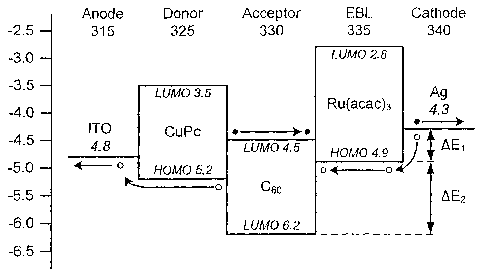
likelihood that excitons
will be generated far from the effective field at a charge-separating
interface, resulting in
enhanced probability of geminate recombination and, again, reduced efficiency.
Therefore, a
device configuration is desirable which balances between these competing
effects in a manner
that produces a high external quantum efficiency for the overall device.
[0074] The organic photosensitive optoelectronic devices may function as
photodetectors. As a
photodetector, the device may be a multilayer organic device, for example as
described in U.S.
Published Patent Application No. 2005-0110007 Al, published May 26, 2005 to
Forrest et al.,
19
CA 02611864 2007-12-12
WO 2006/138078 PCT/US2006/021374
incorporated hereiri by reference in its entirety. In this case an external
electric field may be
generally applied to facilitate extraction of the separated charges.
[0075] A concentrator or trapping configuration can be employed to increase
the efficiency of
the organic photosensitive optoelectronic device, where photons are forced to
make multiple
passes through the thin absorbing regions. U.S. Patent No. 6,333,458 to
Forrest et al. atid U.S.
Patent 6,440,769 to Peumans et al., both incorporated herein by reference in
their entirety,
address this issue by using structural designs that enhance the
photoconversion efficiency of
photosensitive optoelectronic devices by optimizing the optical geometry for
high absorption and
for use with optical concentrators that increase collection efficiency. Such
geometries for
photosensitive devices substantially increase the optical path through the
material by trapping the
incident radiation within a reflective cavity or waveguiding structure, and
thereby recycling light
by multiple reflection through the photoresponsive material. The geometries
disclosed in U.S.
Patent Nos. 6,333,458 and 6,440,769 therefore eiihance the external: quantum
efficiency of the
de.vices: without causing substantial increase in bulk resistance: Jncluded in
the geometry of such.
devices is-a first reflective layer; a transparent insulating layer which
should be Ionger than the
optical coherence -length of the incident light in all dimensions to prevent
optical rnicrocavity'
interference effects; a transparent first electrode layer adjacent the.
transparent insulating layer; a
photosensitive heterostructure adjacent the transparent electrode; and a
second electrode.w.hich-is.
also reflective.
[0076] Coatings may be used to focus optical energy into desired regions of a
device. US Patent
Application No. 10/857,747, filed June 1, 2004, which is incorporated by
reference in its
entirety, provides examples of such a coating.
[0077] Organic photovoltaic (PV) cells have the potential to provide low cost
solar energy
conversion due to their relative ease of processing and compatibility with
flexible substrates.
The photogeneration process in these devices relies on the dissociation of
excitons, or bound
electron-hole pairs, at a donor-acceptor heterojunction (DA-HJ). Excitons,
however, must be
generated sufficiently close to the DA-HJ such that they can diffuse to this
interface before
recombining. Different methods have been employed to avoid this so-called
'exciton diffusion
bottleneck' in small molecular weight organic semiconductor based PV cells,
such as using
mixed DA materials, materials with long exciton diffusion lengths, or by
connecting multiple
devices in a series connection. The performance of such devices utilizing
these various
CA 02611864 2007-12-12
WO 2006/138078 PCT/US2006/021374
strategies has receritly increased dramatically, reaching power conversion
efficiencies (flp) as
high as 5.7% under AM1.5G simulated solar illumination.
[0078] High efficiency small-molecule based devices many times include an
exciton blocking
layer (EBL) inserted between the acceptor-type molecular layer and the
cathode. The EBL
serves a number of functions, including preventing damage to the photoactive
layer during
cathode deposition, thereby eliminating exciton quenching at the
acceptor/cathode interface.
This material should be transparent across the solar spectrum to act as a
spacer between the
photoactive region and the metal interface to allow for increased absorption
at the active DA
interface where photo-induced charge transfer occurs. Furthermore the EBL must
transport
charge to ensure a low cell series resistance and high responsivity. In the
case of a material that
satisfies all of these criteria, the EBL should also be sufficiently thick to
place the region of
highest incident optical light intensity at the DA-HJ, which is located at a
distance of
approximately an integer multiple of wavelengths divided by twice the index of
refraction of the
organic material (k/2n) from the metal cathode, where electrostatic
bourida:ry'conditions demand ;
tliat- the inc'idant=optical field'intensity vanishes. Examples ofthe
relationship between
wavelengtli, -light intensity, and distance from a reflective metal cathode
are shown in.FIG.~ 14.:
By adjustingthe, thickness of an EBL-between-the DA-HJ-and the cathode,'the
position of the
field intensity peaks can be optimized. -
[0079] Also, thick EBLs are practically important for fabricating large-area
devices with a low
density of electrical shorts. Bathocuproine (BCP) has typically been used as
an EBL material in
small molecular-weight organic PVs. However, its large energy gap and
resistance make it
unsuitable for use as a thick layer, where increased cell series resistance
degrades device
performance. Doping the EBL to retain a low series resistance has proven to be
an effective -
solution in allowing the use of thicker EBL layers (see Maennig et al.,
Applied Physics A 79, 1
(2004)), as has the use of a thick 3,4,7,8 napthalenetetracarboacylic
dianhydride layer (see
Suemori, Applied Physics Letters 85, 6269 (2004)).
[0080] Prior to the work described herein, it was believed that BCP was
effective as an EBL
material due to damage-mediated charge transport of electrons. An example of
the theoretical
carrier transport in a device 1100 is illustrated in FIG. 11, in which a
photogenerated electron
travels from the acceptor 1130, by damage-mediated charge transport 1271
through the EBL
1135, to the cathode 1140 and a load 90. As illustrated in FIG. 12, formation
of the Ag cathode
21
CA 02611864 2007-12-12
WO 2006/138078 PCT/US2006/021374
layer 1140 induces damage in the BCP EBL 1135, which was believed to enable
the transport of
electrons from the acceptor 1'130 to the cathode 1140.~ Also illustrated in
FIG. 12 are an anode
1115 and a donor 1125. For an example of damage-induced electron transport
with BCP, see
U.S. Published Patent Application No. 2002/0189666 A1 published December 19,
2002 to
Forrest et al.
[00811 The belief that BCP depended on damage-induced electron transpol-t had
several practical
consequences, iilcluding choice of dopants (if any) and the choice of other
materials that might
be used (e.g., instead of BCP). However, since carrier transport depends upon
cathode-induced
damage, BCP was viewed as unsuitable for thick layers, due the relatively
shallow effectiveness
of the damage, resulting in high resistance for thick layers. This knowledge
acted as a limitation
on the thickness of the EBL, limiting the extent to which the position of the
peak optical intensity
could be adjusted (e.g., FIG. 14). Moreover; BCP-based EBLs were seen as,
unsuitable for most
-inverted devices (devices with the cathode near the substrate), since-an EBL
deposited on the
cathode would not,be damaged, and thus, would have high resistance even as a
thin.layer.
![0082] Research- described hereinreveals that the prevailing theory of damage-
induced,eledtron
#iarisport :through'BCP may be incorrect: New experimental results; -
described,below: and
-illustrated in. FIG. 13, reveal that the'EB.L-1335, is actually transportiing
disassociated-holes via
damage mediated charge transport = 1372- from the cathode 1140 to-the acceptor
1130, with
electron-hole recombination occurring at the acceptor-EBL interface. While the
general theory
regarding damage states being responsible for charge transport in BCP appears
to be correct, the
identity of which carrier is transported may have been incorrect.
[0083] Knowledge that holes disassociate at the cathode to be carried to the
acceptor for
recombination causes us to revisit some of the basic tenets of device design.
Specifically, a
whole new class of materials that had never been considered as usable for an
EBL layer between
the acceptor and the cathode can now be considered. Moreover, if dopant is
added to the EBL
(e.g., to mairitain an amorphous state), the choice of dopants can be better
optimized to
complement the transport of the holes.
[00841 FIGS. 2A and 2B illustrate operation of a device 200 in accordance with
embodiments of
the present invention. A hole disassociates from an electron in cathode 140,
to be transported
through the EBL 135 for recombination at the acceptor-EBL interface. The
orientation of the
22
CA 02611864 2007-12-12
WO 2006/138078 PCT/US2006/021374
device 200 is not important, as it may be a regular (cathode on top) or an
inverted (cathode on
bottom) device.
[0085] Applying this new theory of operation, the characteristic energy levels
of the materials
may be selected as demonstrated with FIG. 2B..
[0086) A first departure from prior designs is the positioti of the HOMO of
the EBL 135 relative
to the HOMO of the acceptor 130 (AEZ). In prior art designs, since EBLs were
designed to
primarily rely upon hole-blocking to prevent exciton quenching, the HOMO of
the acceptor
needed.to be higher (less negative) than the HOMO of the EBL. However, as
embodiments of
the present invention primarily utilize hole transport, the HOMO of the EBL
135 may be,set
higher than or equal to the HOMO of the acceptor 130.
[0087] A second departure from prior designs is the selection of materials for
the EBL that have
a hole mobility of at least 10-7 cm2/V-sec or higher. While dasnaged-ind'uced
carrier transport in
materials su.ch as BCP does not per se rely upon the mobility of the material,
if an undamaged
ixiaterial'was selected to transport carriers through the EBL, carrier
mobility iuould be 'an-
. importarit~ consi'deration: However, it 'follovvs from:the prior art to
maximize the mobility"of ~
electrbiis; rather than holes, since the" phenoxiiena of hole disassociation
at the cathode was not
recognized. This relatively high hole rnobility of at least '10cm2/V-sec or
higher provides a*-'
threshold to avoid domination by EBL resisliv'ity'over the exciton diffusion
bottleneck, which
would degrade device performance. Higher mobilities, such as at least 10-6 em2
/V-se c or higher,
are preferred.
[0088] A third departure from prior designs is the energy level difference AEi
between the Fermi
level (EF) of the cathode 140 and the HOMO of the EBL 135. In the prior art,
the position of the
Fermi level was optimized for the injection of electrons from the EBL into the
cathode.
Applying this new knowledge, the Fermi level may be better optimized for the
injection of holes
from the cathode to the EBL. Preferably, for good injection of holes, the
Fermi level of the
cathode is no more than 1 eV higher than the HOMO of the exciton blocking
layer. More
preferably, the Fermi level of the cathode is not higher than the HOMO. This
may also be
expressed as the work function of the cathode being no more than 1 eV smaller
than the
ionization potential of the EBL, where the ionization potential is the energy
difference between
the vacuum level and the HOMO.
23
CA 02611864 2007-12-12
WO 2006/138078 PCT/US2006/021374
(0089] A fourth departure from prior designs is the energy level difference
AE3 between the
LUMO of the acceptor 130 and the HOMO of the LUMO 135. In the prior art, this
difference
was typically very large, since the HOMO of the EBL was selected to block the
injection of
holes from the acceptor into the EBL (as a means of exciton blocking).
However, since
embodiments of the present invention employ hole transport through the EBL
toward the
acceptor, a larger difference dE3 results in energy lost to electron hole
recombination (e.g.,
phonon generation). Accordingly, rather than employing a large AE3 as in the
prior art to block
holes/excitons, it is preferred that this difference AE3 is minimized.
Preferably, the HOMO of
the exciton blocking layer 135 is no more than I eV below the LUMO of the
acceptor 130.
[0090] Preferably, the material used for the EBL 135 has the hole mobility of
at least 10-7 cm2 /V-
sec or higher in the absence of dopants and impurities. However, that is not
to say that the EBL
135 is not doped. For example, as described above, the EBL 135 may be doped to
help prevent
recrystalization.
:[0091]: So-tong as the EBL 135 blocks excitons and transports holes, the
electron-related
characteristics:of the EBL material are not essentiaL Some electron
transport~can be tolerated; :so-r
long as;excitons.cannotpass, through to quench at:the cathode -140. For
example, not all s..
recombination.need occur at the acceptor-EBL inter.face; recombination may
also occur,irt.the:..;
EBL itself.
[0092] Although the device 200 in FIG. 2A is ilh.istrated as being connected
to a resistive load
90, suggesting a photovoltaic, the presence of the load is purely for
demonstration purposes. In
practice, device 200 can be any type of photosensitive cell, including a
photoconductor cell (in
which case the device would be connected to signal detection circuitry to
monitor changes in
resistance across the device due to the absorption of light) or a
photodetector (in which case the
device would be connected to a current detecting circuit which measures the
current generated
when the photodetector is exposed to light, and in which a bias voltage might
be applied to the
device). This is also true for the devices in the other drawings.
[0093] Although intervening layers such as smoothing layer 120 is not shown in
FIG. 2A, other
layers may be present. This is also true for the devices in the other
drawings.
24
CA 02611864 2007-12-12
WO 2006/138078 PCT/US2006/021374
Experiments -
[0094] An experimental device architecture 300 is illustrated in FIGS. 3A and
3B which satisfies
the preferred parasneters for embodiments of the present invention. C60 was
selected as the
acceptor 330, tris(acetylacetonato)ruthenium(III) (Ru(acac)3) as the EBL
material 335, and Ag as
the cathode 340. Additionally, ITO was used as the anode 315, CuPC was used as
the donor
325, atld the substrate 310 was glass. In comparison to a BCP-based device,
the thickness of
EBL 335 can be increased without a loss in power conversion efficiency.
[0095] To understand differences in blocking layer performance between BCP-and
Ru(acac)3-
based devices, ultraviolet photoelectron spectroscopy (UPS) was used to
measure the offset
energy of the highest occupied molecular orbital (HOMO) level at the C60/EBL
interface, and
confirm previous studies that show that charge transport in BCP is due to
damage induced during
deposition of the Ag cathode, while the small ionization potential of
Ru(acac)3 allows for hole
transport to the type II C60/Ru(acac)3 HJ where recombination with
photogenerated electrons can
occur.
j00961 Figure'4 'shovvs'the current density-voltage- (J-V),characteristics in
the dark anduh'der 1
"sun (1,0'C1mW/cm2) AM1.5G simulated solar illumiination for devices with the
structure
;
ITO/CuPc/Cdo/EBL(200A)/Ag (ITO: 'indium tin oxide; CuPc: copper
phthalocyacine), where the "
EBL consists of either BCP (filled circles) or Ru(acac)3 (open squares). From
fits of the dark J=
V characteristics to classical p-n junction diode theorya. series resistance
Rs = 40.6 Qem2 and Rs
= 3.6 ncrn2 and ideality factors of n =2.2 0.1 and n=1.9 0.1 can be
inferred for the BCP and
Ru(aca.c)3 devices, respectively. Under I sun illumination, the responsivity
(equal to Jsc / Po,
where JsC is the short circuit current density and Po is the incident light
intensity) of the BCP and
Ru(acac)3 devices are (0.07 0.01) A/W and (0.09 0.01) A/W with fill
factors equal to FF =
0.29 0.02 and FF = 0.58 + 0.03, respectively. An open circuit voltage of Voc
=(0.52 0.02) V
is obtained for both devices. These characteristics result in cell power
conversion efficiencies,
i1P =(VocJscFF)/Po, of rlP =(1.1 10.1)% and (2.7 0.2)% for 200-A-thick BCP.
and Ru(acac)3
EBL devices..
[0097] Figures 5A and 5B show responsivity and FF, respectively, as a function
of EBL
thickness for the device structure in 4. Note that devices lacking an EBL have
both a low
responsivity and FF due to quenching at the C60/Ag interface as well as at
defects induced during
Ag deposition on the C60 surface. The BCP and Ru(acac)3 devices show a peak in
performance
CA 02611864 2007-12-12
WO 2006/138078 PCT/US2006/021374
at a thiclrness of 100 A. However, the responsivity and FF of the BCP devices
decrease rapidly
for larger EBL thicknesses whereas the responsivity of the Ru(acac)3 device
falls off more gently
due to a decrease in optical intensity at the DA interface with increasing
thickness. This effect is
accurately predicted using models introduced elsewhere (solid line, FIG. 5A).
The deviation
frorn the optical model at EBL thicluiesses < 50 A is due to exciton quenching
at the C60/Ag
interface.
[0098] Ultraviolet Photoelectron Spectroscopy (UPS) was used to study the
evolution of the
,HOMO, or ionization potential, of the organic interface between C60 and the
EBL as a means to
understand these two double-heterostructure PV cells. The evolution of the UPS
spectra of an
overlayer of BCP on a 200-A-thick C60 film shown in FIG. 6. The UPS spectrum
of neat films
of C60 (bottom spectrum, FIG. 6) and BCP yield HOMO levels of (6.2 + 0.1) eV
and (6.5 0.1)
eV, respectively, in agreement with literature values (see Hill et al.,
Journal Applied Physics 86,
4515 (1999); Mitsumoto et al., Journal of Physical Chemistry A 102, 552
(1998)). As can be
seen in FIG. 6, the deposition of increasing amounts of BCP on C6n results in
a rigid shift of the
spectrum toward higher binding energy. . This is caused.ei.ther... by, -band-
bending, or by charging :
within the wide energy gap :BCP layer. By fitting the: UPS.. speetrum at BCP
overlayer .
thiclcnesses of 8.azid 16 Ato a Gaussian shape, a HOMO.level offset of -0.3
eV.toward higher ;=
binding energy can be inferred, indicating that the vacuum levels at the
C60/BCP interface align.
Upon deposition of a 32 A BCP overlayer, the UPS spectrum resembles that of
neat BCP,
indicating that the C60 is completely covered.
[0099] The spectrum of neat Ru(acac)3 and the evolution of the C60/Ru(acac)3
HJ are shown in
FIG. 7. The HOMO level of Ru(acac)3 is measured as (4.9 0.1) eV. Upon
deposition of a thin
layer Ru(acac)3 on C60, another rigid shift of the spectrum is observed due to
band-bending or
charging effects. The HOMO of Ru(acac)3 is (1.3 0.1) eV lower than that of
C60, indicating the
alignment of the vacuum levels at the C60/R.u(acac)3 interface without the
presence of an
appreciable interface dipole.
[00100] The UPS results suggest the energy diagrams in FIG. 3B and FIG. 13 of
the two
double HJ PV cells. Here, the HOMO energies are taken from UPS measurements,
whereas the
lowest unoccupied molecular orbital (LUMO) energies are estimated using the
optical energy
gap of each material. In the case of the BCP device (FIG. 13), the Ag cathode
deposition allows
for damage-mediated charge transport of carriers through the BCP layer. As
shown previously,
26
CA 02611864 2007-12-12
WO 2006/138078 PCT/US2006/021374
the damage depth i's -100A, with thicker BCP EBLs resulting in reduced
photocurrent (c.f. FIG.
5A). Note that the LUMO-LUMO offset between C60 and the EBL is approximately
the same
for both materials, -0.5 4- 0.1) eV for C60BCP and -(1.7 0.1) eV for
C6o/Ru(acac)3.
Therefore, it is unlikely that photogenerated electrons are transported
through the Ru(acac)3
layer. FurChermore, the hole conductivity of Ru(acac)3 is measured to be ai, =
2.2 x10"' S/cm,
which exceeds that of electrons by two orders of magnitude. However, the
energy alignment
suggests that holes can be injected from the Ag cathode into the Ru(acac)3
layer (FIG. 3B),
where they are transported prior to recombination with electrons at the
C60/Ru(acac)3 interface.
[00101] To confirm this process, the performance of two devices were compared
with the
following layer structures; Device A: ITO/CuPc/C60/Ru(acac)3BCP/Ag and Device
B:
ITO/CuPc/C60BCP/Ru(acac)3/Ag. The responsivity of these two devices are shown
in FIG. 8.
The Device A, consistin-g of a Ru(acac)3/BCP EBL, has a responsivity
equivalent to a device
containing only a BCP EBL for Ru(acac)3 thicknesses of up to 300 A. The Device
B, has a
responsivity three orders of magnitude' below that of Device A for any
Ru(acac)3 layer thickness.
This is due to the inability for photogenerated electroris to be transported
to tliecathode since
damage to the BCP layer during the.Ag cdthode deposition was--prevented:by-the
Ru(acac)3 cap:..
' In contrast, BCP is 'able to transport:-holes to the,Ru(acac)3 laye'r.: via
damage induced.defect
states in Device A; as suggested in FIG. 13.
[001021 Small moleci.alar weight PV cells used to study EBL properties were
fabricated on
1500-A-thick layers of ITO commercially precoated onto glass substrates with a
sheet resistance
of 15 0/square. The solvent cleaned ITO surface was treated in ultraviolet/03
for 5 minutes
immediately before loading the substrates into a high vacuum chamber (-3 x
10"7 Torr), where
organic layers and a Ag cathode were deposited via thermal evaporation. A
quartz crystal
monitor was used to determine film thickness and deposition rate. Prior to
deposition, the
organic materials were purified in three cycles using vacuum thermal gradient
sublimation. The
device structure consists of a 200-A-thick layer of the donor, CuPc, a 400-A-
thick C60 acceptor
layer, and an EBL consisting of either BCP (see FIG. 6, inset) or Ru(acac)3
(see FIG. 7, inset).
Finally, a 1000-.A-thick Ag cathode was evaporated through a shadow mask with
1 mm diameter
openings. The J-V characteristics were measured in the dark and under
simulated AM1.5G solar
illumination (Oriel Instruments) using an HP4155B semiconductor parameter
analyzer.
Illumination intensity was measured using a calibrated broadband optical power
meter. Organic
27
CA 02611864 2007-12-12
WO 2006/138078 PCT/US2006/021374
material studied wi't11 UPS were grown by ultrahigh vacuum organic molecular
beam deposition
on highly doped n-Si(100) substrates coated with 500-A-thick in situ deposited
Ag layers. Hel
emission (21.22 eV) from a VG UPS/21amp (Thermo VG Scientific) was used as a
photon
source, and the spectra were collected with a multichannel hemispherical VG
CLAM4 electron
energy analyzer. The UPS measurement resolution is 0.1 eV.
[00103] Although not actually fabricated, FIGS. 9A and 9B demonstrate an
inverted device
90. The substrate 901 may or may not,be transparent. Similarly; FIGS. IOA and
1 B
demonstrate a device 1000 employing a composite cathode 1040. Any type of
composite
cathode 1040 may be used, as described above. In this example, the composite
cathode
eomprises a thin metallic cathode 1041 and a non-metallic cathode 1042. For
the non-metallic
cathode 1042, room-temperature sputtered ITO without surface treatment (ITO*)
is used to
achieve a work function commensurate with a metaL cathode. The work function
for ITO* may
be as low as 4.0 eV to 4.3 eV. In comparison, commercially obtained ITO and
the ITO usea for
the anode received a surface treatment UV-ozone, oxygen plasma) to obtain a
work
function of 4.8 eV. . Although device.10:q0..is_zhawn
with:a.transparent:;anode -and- substrate, a
reflective anode (e.g., gold),..intervening::lay.er, orsubstrateinateri
al.may..be.used. Likewise,.in
- FIG. 9, a transparent cathode (e.g., ITO.*)..iand substrate ma.y be-used,
and either the:anode.may
be made reflective (e.g., gold),.or a reflective layer may be. added. .
[00104] o In conclusion, an efficient organic dou:ble-heterostructure
photovoltaic cell has been
demonstrated employing an exciton blocking layer which does not rely on
cathode induced
damage for charge transport. By experiments, it has been found that high power
conversion
efficiencies are obtained for Ru(acac)3 thicknesses up to 300 A, whereas BCP-
based devices
experience a rapid falloff of both responsivity and fill factor at these large
thicknesses. Since the
Ru(acac)3 exciton blocking layer functionality is due to energy level
alignment rather than metal
deposition-induced damage, its thickness can be optimally designed to position
the charge
generating layers in the region of highest incident light intensity, thereby
maximizing the power
conversion efficiency in the characteristically thin organic layers used in
organic solar cells
while reducing the possibility of electrical shorts in large area devices.
[00105] Although the present invention is described with respect to particular
examples and
embodiments, it is understood that the present invention is not limited to
these examples and
embodiments. The present invention as claimed may therefore include variations
from the
28
CA 02611864 2007-12-12
WO 2006/138078 PCT/US2006/021374
particular examples and preferred embodiments described herein, as will be
apparent to one of
skill in the art.
29