Note : Les descriptions sont présentées dans la langue officielle dans laquelle elles ont été soumises.
CA 02615919 2008-01-18
WO 2007/015861
PCT/US2006/027844
HEATABLE WINDSHIELD
BACKGROUND OF THE INVENTION
1. Field of the Invention
[0001] This invention relates generally to vehicle transparencies, such
as
vehicle windshields, and, in one particular embodiment, to a heatable vehicle
windshield.
2. Technical Considerations
[0002] It has been known to pass electric current through a conductor
(e.g., a
wire or an electrically conductive coating) on a laminated vehicle windshield
in order
to raise the temperature of the windshield. This is particularly useful in
colder
climates for defogging and to melt ice and snow on the windshield.
[0003] In wire-heated windshields, fine electrically-conductive wires are
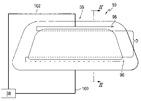
placed
between the windshield plies. The wires are connected to a power source, such
as a
conventional 14 volt (v) vehicle alternator. The wires have sufficiently low
resistance
to provide the windshield with a power density of 5 to 7 watts per decimeter
squared
(W/d m2).
[0004] However, a problem with wire-heated windshields is that the wires
can
be seen by the vehicle occupants. The presence of these wires can be
aesthetically
undesirable and can interfere with visibility through the windshield. If the
diameter of
the wires is decreased to try to reduce the visibility of the wires, the
number of wires
must be increased to maintain the desired power density. The increased number
of
wires adversely decreases the total solar energy transmitted (TSET) of the
windshield. If the height of the windshield increases, the wires must be
longer to
maintain the desired power density. These longer wires are also undesirable
with
respect to windshield aesthetics and/or transmittance.
[0005] In an effort to address this problem, some heated windshields
utilize
transparent, conductive coatings rather than wires to heat the windshield.
While
these known transparent coatings overcome the aesthetic and visibility
problems
associated with the use of wires, conventional heated windshield coatings also
have
some drawbacks. For example, conventional heated windshield coatings typically
have a sheet resistance of 2 ohms per square (0/12) or greater. A conventional
14v
CA 02615919 2008-01-18
WO 2007/015861
PCT/US2006/027844
- 2 -
(80 ampere; 1,120 watts) alternator does not provide sufficient voltage to
power a
conventional heated windshield coating to a temperature sufficient for de-
icing.
Therefore, for vehicles with these conventional coatings, the vehicles must be
altered to increase the available voltage. One way to do this is to replace
the
conventional 14v (1,120 W) alternator with a 42v (2,500 W to 5,000 W)
alternator.
Another way to address this problem is to maintain the conventional 14v
alternator
but add a DC to DC converter to step up the voltage to a sufficient level,
e.g., 42v, to
heat the windshield to a commercially acceptable level.
[0006] However, replacing the conventional 14v alternator or adding a DC
to
DC converter increases the cost and complexity of the vehicle electrical
system.
Also, as one skilled in the art will appreciate, all things being equal, a
system that
functions on 14 volts is typically safer to operate than one that operates on
42 volts.
[0007] Therefore, it would be desirable to provide a transparency, such as
a
laminated vehicle transparency, that reduces or eliminates at least some of
the
problems associated with conventional heatable transparencies.
SUMMARY OF THE INVENTION
[0008] A heatable transparency of the invention comprises a first ply
having a
No. 1 surface and a No. 2 surface and a second ply having a No. 3 surface and
a
No. 4 surface. The No. 2 surface faces the No. 3 surface. A conductive coating
is
formed on the No. 2 or No. 3 surface. A power supply is in contact with the
conductive coating. The system is configured such that the power supply
provides
less than 42 volts to the conductive coating. In one non-limiting embodiment,
the
system is configured such that the power supply provides less than 24 volts,
such as
in the range of 13 volts to 15 volts to the conductive coating. In one non-
limiting
embodiment, the coating provides a power density in the range of 4 W/dm2 to 8
W/dm2, e.g., 5 W/dm2 to 7 W/dm2.
[0009] A further heatable transparency comprises a first ply having a No.
1
surface and a No. 2 surface and a second ply having a No. 3 surface and a No.
4
surface. The No. 2 surface faces the No. 3 surface. A conductive coating is
formed
on the No. 2 or No. 3 surface, with the conductive coating comprising three or
more
metallic silver layers. An antireflective coating can be formed on the No. 4
surface.
CA 02615919 2008-01-18
WO 2007/015861
PCT/US2006/027844
- 3 -
[0010] A further heatable laminated transparency comprises a first ply
having
a No. 1 surface and a No. 2 surface and a second ply having a No. 3 surface
and a
No. 4 surface. The No. 2 surface faces the No. 3 surface. A conductive coating
is
formed on the No. 2 or No. 3 surface. The conductive coating comprises three
or
more metallic silver layers and the conductive coating is configured to
provide a
resistivity in the range of 0.6 CVO to 1.70 CVO. An antireflective coating is
formed on
the No. 4 surface. In one embodiment, the antireflective coating comprises at
least
one zinc stannate layer and at least one zinc oxide layer. The laminated
transparency can have a visible light transmittance of greater than or equal
to 70% at
a reference wavelength of 550 nm.
BRIEF DESCRIPTION OF THE DRAWINGS
[0011] The invention will be described with reference to the following
drawing
figures wherein like reference numbers identify like parts throughout.
[0012] Fig. 1 is a schematic view (not to scale) of a heatable windshield
incorporating features of the invention;
[0013] Fig. 2 is an expanded view (not to scale) of the windshield taken
along
the line II-II of Fig. 1;
[0014] Fig. 3 is a cross-sectional view (not to scale) of a non-limiting
conductive coating suitable for the invention;
[0015] Fig. 4 is a cross-sectional view (not to scale) of a non-limiting
antireflective coating suitable for the invention; and
[0016] Fig. 5 is a schematic view (not to scale) of another windshield
incorporating features of the invention.
DESCRIPTION OF THE PREFERRED EMBODIMENTS
[0017] As used herein, spatial or directional terms, such as "left",
"right",
"inner", "outer", "above", "below", and the like, relate to the invention as
it is shown in
the drawing figures. However, it is to be understood that the invention can
assume
various alternative orientations and, accordingly, such terms are not to be
considered as limiting. Further, as used herein, all numbers expressing
dimensions,
physical characteristics, processing parameters, quantities of ingredients,
reaction
CA 02615919 2008-01-18
WO 2007/015861 PCT/US2006/027844
- 4 -
conditions, and the like, used in the specification and claims are to be
understood as
being modified in all instances by the term "about". Accordingly, unless
indicated to
the contrary, the numerical values set forth in the following specification
and claims
may vary depending upon the desired properties sought to be obtained by the
present invention. At the very least, and not as an attempt to limit the
application of
the doctrine of equivalents to the scope of the claims, each numerical value
should
at least be construed in light of the number of reported significant digits
and by
applying ordinary rounding techniques. Moreover, all ranges disclosed herein
are to
be understood to encompass the beginning and ending range values and any and
all
subranges subsumed therein. For example, a stated range of "1 to 10" should be
considered to include any and all subranges between (and inclusive of) the
minimum
value of 1 and the maximum value of 10; that is, all subranges beginning with
a
minimum value of 1 or more and ending with a maximum value of 10 or less,
e.g., 1
to 3.3,4.7 to 7.5, 5.5 to 10, and the like. Further, as used herein, the terms
"formed
over", "deposited over", or "provided over" mean formed, deposited, or
provided on
but not necessarily in contact with the surface. For example, a coating layer
"formed
over" a substrate does not preclude the presence of one or more other coating
layers
or films of the same or different composition located between the formed
coating
layer and the substrate. As used herein, the terms "polymer" or "polymeric"
include
oligomers, homopolymers, copolymers, and terpolymers, e.g., polymers formed
from
two or more types of monomers or polymers. The terms "visible region" or
"visible
light" refer to electromagnetic radiation having a wavelength in the range of
380 nm
to 800 nm. The terms "infrared region" or "infrared radiation" refer to
electromagnetic
radiation having a wavelength in the range of greater than 800 nm to 100,000
nm.
The terms "ultraviolet region" or "ultraviolet radiation" mean electromagnetic
energy
having a wavelength in the range of 300 nm to less than 380 nm. Additionally,
all
documents, such as but not limited to issued patents and patent applications,
referred to herein are to be considered to be "incorporated by reference" in
their
entirety. The "visible transmittance" and "dominant wavelength" values are
those
determined using the conventional methods. Those skilled in the art will
understand
that properties such as visible transmittance and dominant wavelength can be
CA 02615919 2008-01-18
WO 2007/015861
PCT/US2006/027844
- 5 -
calculated at an equivalent standard thickness, e.g., 5.5 mm, even though the
actual
thickness of a measured glass sample is different than the standard thickness.
[0018] For purposes of the following discussion, the invention will be
discussed with reference to use with a vehicle transparency, in particular an
automotive windshield. However, it is to be understood that the invention is
not
limited to use with vehicle windshields but could be practiced in any desired
field,
such as but not limited to laminated or non-laminated residential and/or
commercial
windows, insulating glass units, and/or transparencies for land, air, space,
above
water and under water vehicles, e.g., automotive windshields, sidelights, back
lights,
sunroofs, and moon roofs, just to name a few. Therefore, it is to be
understood that
the specifically disclosed exemplary embodiments are presented simply to
explain
the general concepts of the invention and that the invention is not limited to
these
specific exemplary embodiments. Additionally, while a typical vehicle
"transparency"
can have sufficient visible light transmittance such that materials can be
viewed
through the transparency, in the practice of the invention the "transparency"
need not
be transparent to visible light but may be translucent or opaque (as described
below). Non-limiting examples of vehicle windshields and methods of making the
same are found in U.S. Patent Nos. 4,820,902; 5,028,759; and 5,653,903.
[0019] A non-limiting heatable transparency 10 (e.g., automotive
windshield)
incorporating features of the invention is illustrated in Figs. 1 and 2. The
transparency 10 can have any desired visible light, infrared radiation, or
ultraviolet
radiation transmission and reflection. For example, the transparency 10 can
have a
visible light transmission of any desired amount, e.g., greater than 0% to
100%, e.g.,
greater than 70%. For windshield and front sidelight areas in the United
States, the
visible light transmission is typically greater than or equal to 70%. For
privacy areas,
such as rear seat sidelights and rear windows, the visible light transmission
can be
less than that for windshields, such as less than 70%.
[0020] As best seen in Fig. 2, the transparency 10 includes a first ply
12 with a
first major surface facing the vehicle exterior, i.e., an outer major surface
14 (No. 1
surface) and an opposed second or inner major surface 16 (No. 2 surface). The
transparency 10 also includes a second ply 18 having an outer (first) major
surface
20 (No, 3 surface) and an inner (second) major surface 22 (No. 4 surface).
This
CA 02615919 2008-01-18
WO 2007/015861
PCT/US2006/027844
- 6 -
numbering of the ply surfaces is in keeping with conventional practice in the
automotive art. The first and second plies 12, 18 can be bonded together in
any
suitable manner, such as by a conventional interlayer 24. Although not
required, a
conventional edge sealant can be applied to the perimeter of the laminated
transparency 10 during and/or after lamination in any desired manner. A
decorative
band, e.g., an opaque, translucent or colored shade band 26 (shown in Fig. 2),
such
as a ceramic band, can be provided on a surface of at least one of the plies
12, 18,
for example around the perimeter of the inner major surface 16 of the first
ply 12. An
electrically conductive coating 30 is formed over at least a portion of one of
the plies
12, 18, such as over the No. 2 surface 16 or No. 3 surface 20. An
antireflective
coating 32 is formed over at least one of the surfaces, such as over the No. 4
surface 22. A bus bar assembly 36 (Fig. 1) is in electrical contact with the
conductive coating 30. The bus bar assembly 36 is also connected to an
electrical
power source 38 (Fig. 1) and will be discussed in more detail below. In one
non-
limiting aspect of the invention, the power source 38 can be a conventional
vehicle
alternator, e.g., configured to supply approximately 14 volts. Thus, in the
practice of
one non-limiting embodiment of the invention, no DC to DC power converter is
present, as is required in the known art.
[0021] In the broad practice of the invention, the plies 12, 18 of the
transparency 10 can be of the same or different materials. The plies 12, 18
can
include any desired material having any desired characteristics. For example,
one or
more of the plies 12, 18 can be transparent or translucent to visible light.
By
"transparent" is meant having visible light transmittance of greater than 0%
to 100%.
Alternatively, one or more of the plies 12, 18 can be translucent. By
"translucent" is
meant allowing electromagnetic energy (e.g., visible light) to pass through
but
diffusing this energy such that objects on the side opposite the viewer are
not clearly
visible. Examples of suitable materials include, but are not limited to,
plastic
substrates (such as acrylic polymers, such as polyacrylates;
polyalkylmethacrylates,
such as polymethylmethacrylates, polyethylmethacrylates,
polypropylmethacrylates,
and the like; polyurethanes; polycarbonates; polyalkylterephthalates, such as
polyethyleneterephthalate (PET), polypropyleneterephthalates,
polybutyleneterephthalates, and the like; polysiloxane-containing polymers; or
CA 02615919 2008-01-18
WO 2007/015861 PCT/US2006/027844
- 7 -
copolymers of any monomers for preparing these, or any mixtures thereof);
ceramic
substrates; glass substrates; or mixtures or combinations of any of the above.
For
example, one or more of the plies 12, 18 can include conventional soda-lime-
silicate
glass, borosilicate glass, or leaded glass. The glass can be clear glass. By
"clear
glass" is meant non-tinted or non-colored glass. Alternatively, the glass can
be
tinted or otherwise colored glass. The glass can be annealed or heat-treated
glass.
As used herein, the term "heat treated" means tempered or at least partially
tempered. The glass can be of any type, such as conventional float glass, and
can
be of any composition having any optical properties, e.g., any value of
visible
transmission, ultraviolet transmission, infrared transmission, and/or total
solar energy
transmission. By "float glass" is meant glass formed by a conventional float
process
in which molten glass is deposited onto a molten metal bath and controllably
cooled
to form a float glass ribbon. The ribbon is then cut and/or shaped and/or heat
treated as desired. Examples of float glass processes are disclosed in U.S.
Patent
Nos. 4,466,562 and 4,671,155. The first and second plies 12, 18 can each be,
for
example, clear float glass or can be tinted or colored glass or one ply 12, 18
can be
clear glass and the other ply 12, 18 colored glass. Although not limiting to
the
invention, examples of glass suitable for the first ply 12 and/or second ply
18 are
described in U.S. Patent Nos. 4,746,347; 4,792,536; 5,030,593; 5,030,594;
5,240,886; 5,385,872; and 5,393,593. The first and second plies 12, 18 can be
of
any desired dimensions, e.g., length, width, shape, or thickness. In one
exemplary
automotive transparency, the first and second plies can each be 1 mm to 10 mm
thick, e.g., 1 mm to 5 mm thick, or 1.5 mm to 2.5 mm, or 1.8 mm to 2.3 mm. In
one
non-limiting embodiment, the first ply 12 and/or second ply 18 can have a
visible light
transmittance of greater than 90%, such as greater than 91%, at a reference
wavelength of 550 nm. The glass composition for the first ply 12 and/or second
ply
18 can have a total iron content in the range of greater than 0 wt.% to 0.2
wt.%
and/or a redox ratio in the range of 0.3 to 0.6.
[0022] In one non-limiting embodiment, one or both of the plies 12, 18
may
have a high visible light transmittance at a reference wavelength of 550
nanometers
(nm). By "high visible light transmittance" is meant visible light
transmittance at 550
nm greater than or equal to 85%, such as greater than or equal to 87%, such as
CA 02615919 2008-01-18
WO 2007/015861 PCT/US2006/027844
- 8 -
greater than or equal to 90%, such as greater than or equal to 91%, such as
greater
than or equal to 92%, at 5.5 mm equivalent thickness for glass from 2 mm to 25
mm
sheet thickness. Particularly useful glass for the practice of the invention
is
disclosed in U.S. Patent Nos. 5,030,593 and 5,030,594 and is commercially
available from PPG Industries, Inc. under the mark Starphire .
[0023] The interlayer 24 can be of any desired material and can include
one or
more layers or plies. The interlayer 24 can be a polymeric or plastic
material, such
as, for example, polyvinylbutyral, plasticized polyvinyl chloride, or multi-
layered
thermoplastic materials including polyethyleneterephthalate, etc. Suitable
interlayer
materials are disclosed, for example but not to be considered as limiting, in
U.S.
Patent Nos. 4,287,107 and 3,762,988. The interlayer 24 secures the first and
second plies 12, 18 together, provides energy absorption, reduces noise, and
increases the strength of the laminated structure. The interlayer 24 can also
be a
sound-absorbing or attenuating material as described, for example, in U.S.
Patent
No. 5,796,055. The interlayer 24 can have a solar control coating provided
thereon
or incorporated therein or can include a colored material to reduce solar
energy
transmission.
[0024] The coating 30 is an electrically conductive coating deposited over
at
least a portion of a major surface of one of the glass plies 12, 18, such as
on the
inner surface 16 of the outboard glass ply 12 (Fig. 2) or the outer surface 20
of the
inner glass ply 18. The conductive coating 30 can include one or more metallic
films
positioned between pairs of dielectric layers applied sequentially over at
least a
portion of one of the glass plies 12, 18. The conductive coating 30 can be a
heat
and/or radiation reflecting coating and can have one or more coating layers or
films
of the same or different composition and/or functionality. As used herein, the
term
"film" refers to a coating region of a desired or selected coating
composition. A
"layer" can comprise one or more "films" and a "coating" or "coating stack"
can
comprise one or more "layers". For example, the conductive coating 30 can be a
single layer coating or a multi-layer coating and can include one or more
metals,
non-metals, semi-metals, semiconductors, and/or alloys, compounds,
compositions,
combinations, or blends thereof. For example, the conductive coating 30 can be
a
single layer metal oxide coating, a multiple layer metal oxide coating, a non-
metal
CA 02615919 2008-01-18
WO 2007/015861
PCT/US2006/027844
- 9 -
oxide coating, a metallic nitride or oxynitride coating, a non-metallic
nitride or
oxynitride coating, or a multiple layer coating comprising one or more of any
of the
above materials. In one non-limiting embodiment, the conductive coating 30 can
be
a doped metal oxide coating.
[0025] The coating 30 can be a functional coating. As used herein, the
term
"functional coating" refers to a coating that modifies one or more physical
properties
of the substrate over which it is deposited, e.g., optical, thermal, chemical
or
mechanical properties, and is not intended to be entirely removed from the
substrate
during subsequent processing. The conductive coating 30 can have one or more
functional coating layers or films of the same or different composition or
functionality.
[0026] The conductive coating 30 can be, for example, an electrically
conductive coating used to make heatable windows as disclosed in U.S. Patent
Nos.
5,653,903 and 5,028,759, or a single-film or multi-film coating used as an
antenna.
Likewise, the conductive coating can be a conductive, solar control coating.
As used
herein, the term "solar control coating" refers to a coating comprised of one
or more
layers or films that affect the solar properties of the coated article, such
as but not
limited to the amount of solar radiation, for example, visible, infrared, or
ultraviolet
radiation, reflected from, absorbed by, or passing through the coated article,
shading
coefficient, emissivity, etc. The solar control coating can block, absorb or
filter
selected portions of the solar spectrum, such as but not limited to the IR,
UV, and/or
visible spectrums. Examples of solar control coatings that can be used in the
practice of the invention are found, for example but not to be considered as
limiting,
in U.S. Patent Nos. 4,898,789; 5,821,001; 4,716,086; 4,610,771; 4,902,580;
4,716,086; 4,806,220; 4,898,790; 4,834,857; 4,948,677; 5,059,295; and
5,028,759,
and also in U.S. Patent Application Serial No. 09/058,440.
[0027] The conductive coating 30 can also be an electroconductive low
emissivity coating that allows visible wavelength energy to be transmitted
through
the coating but reflects longer wavelength solar infrared energy. By "low
emissivity"
is meant emissivity less than 0.4, such as less than 0.3, such as less than
0.2, such
as less than 0.1, e.g., less than or equal to 0.05. Examples of low emissivity
coatings are found, for example, in U.S. Patent Nos. 4,952,423 and 4,504,109
and
British reference GB 2,302,102.
CA 02615919 2008-01-18
WO 2007/015861
PCT/US2006/027844
- 10 -
[0028] Non-limiting examples of suitable conductive coatings 30 for use
with
the invention are commercially available from PPG Industries, Inc. of
Pittsburgh,
Pennsylvania under the SUNGATE@ and SOLARBAN@ families of coatings. Such
coatings typically include one or more antireflective coating films comprising
dielectric or anti-reflective materials, such as metal oxides or oxides of
metal alloys,
which are transparent to visible light. The conductive coating 30 can also
include
one or more infrared reflective films comprising a reflective metal, e.g., a
noble metal
such as gold, copper or silver, or combinations or alloys thereof, and can
further
comprise a primer film or barrier film, such as titanium, as is known in the
art, located
over and/or under the metal reflective layer. The conductive coating 30 can
have
any desired number of infrared reflective films, such as but not limited to 1
to 5
infrared reflective films. In one non-limiting embodiment, the coating 30 can
have 1
or more silver layers, e.g., 2 or more silver layers, e.g., 3 or more silver
layers, such
as 5 or more silver layers. A non-limiting example of a suitable coating
having three
silver layers is disclosed in U.S. Patent Application Serial No. 10/364,089
(Publication No. 2003/0180547 Al).
[0029] The conductive coating 30 can be deposited by any conventional
method, such as but not limited to conventional chemical vapor deposition
(CVD)
and/or physical vapor deposition (PVD) methods. Examples of CVD processes
include spray pyrolysis. Examples of PVD processes include electron beam
evaporation and vacuum sputtering (such as magnetron sputter vapor deposition
(MSVD)). Other coating methods could also be used, such as but not limited to
sol-
gel deposition. In one non-limiting embodiment, the conductive coating 30 can
be
deposited by MSVD. Examples of MSVD coating devices and methods will be well
understood by one of ordinary skill in the art and are described, for example,
in U.S.
Patent Nos. 4,379,040; 4,861,669; 4,898,789; 4,898,790; 4,900,633; 4,920,006;
4,938,857; 5,328,768; and 5,492,750.
[0030] An exemplary non-limiting coating 30 suitable for the invention is
shown in Fig. 3. This exemplary coating 30 includes a base layer or first
dielectric
layer 40 deposited over at least a portion of a major surface of a substrate
(e.g., the
No. 2 surface 16 of the first ply 12). The first dielectric layer 40 can
comprise one or
more films of antireflective materials and/or dielectric materials, such as
but not
CA 02615919 2008-01-18
WO 2007/015861
PCT/US2006/027844
- 1 1 -
limited to metal oxides, oxides of metal alloys, nitrides, oxynitrides, or
mixtures
thereof. The first dielectric layer 40 can be transparent to visible light.
Examples of
suitable metal oxides for the first dielectric layer 40 include oxides of
titanium,
hafnium, zirconium, niobium, zinc, bismuth, lead, indium, tin, and mixtures
thereof.
These metal oxides can have small amounts of other materials, such as
manganese
in bismuth oxide, tin in indium oxide, etc. Additionally, oxides of metal
alloys or
metal mixtures can be used, such as oxides containing zinc and tin (e.g., zinc
stannate), oxides of indium-tin alloys, silicon nitrides, silicon aluminum
nitrides, or
aluminum nitrides. Further, doped metal oxides, such as antimony or indium
doped
tin oxides or nickel or boron doped silicon oxides, can be used. The first
dielectric
layer 40 can be a substantially single phase film, such as a metal alloy oxide
film,
e.g., zinc stannate, or can be a mixture of phases composed of zinc and tin
oxides or
can be composed of a plurality of metal oxide films, such as those disclosed
in U.S.
Patent Nos. 5,821,001; 4,898,789; and 4,898,790.
[0031] In the illustrated exemplary embodiment shown in Fig. 3, the first
dielectric layer 40 can comprise a multi-film structure having a first film
42, e.g., a
metal alloy oxide film, deposited over at least a portion of the inner major
surface 16
of the first ply 12 and a second film 44, e.g., a metal oxide or oxide mixture
film,
deposited over the first metal alloy oxide film 42. In one non-limiting
embodiment,
the first film 42 can be a zinc/tin alloy oxide. The zinc/tin alloy oxide can
be that
obtained from magnetron sputtering vacuum deposition from a cathode of zinc
and
tin that can comprise zinc and tin in proportions of 10 wt.% to 90 wt.% zinc
and 90
wt.% to 10 wt.% tin. One suitable metal alloy oxide that can be present in the
first
film 42 is zinc stannate. By "zinc stannate" is meant a composition of ZnxSn1-
x02-x
(Formula 1) where "x" varies in the range of greater than 0 to less than 1.
For
instance, "x" can be greater than 0 and can be any fraction or decimal between
greater than 0 to less than 1. For example where x = 2/3, Formula 1 is
Zn2/3Sn1/304/3, which is more commonly described as "Zn2Sn04". A zinc stannate-
containing film has one or more of the forms of Formula 1 in a predominant
amount
in the film. In one non-limiting embodiment, the first film 42 comprises zinc
stannate
and has a thickness in the range of 100 A to 500 A, such as 150 A to 400 A,
e.g.,
200 A to 300 A, e.g., 260 A.
CA 02615919 2008-01-18
WO 2007/015861
PCT/US2006/027844
- 12 -
[0032] The second film 44 can be a zinc-containing film, such as zinc
oxide.
The zinc oxide film can be deposited from a zinc cathode that includes other
materials to improve the sputtering characteristics of the cathode. For
example, the
zinc cathode can include a small amount (e.g., less than 10 wt.%, such as
greater
than 0 to 5 wt.%) of tin to improve sputtering. In which case, the resultant
zinc oxide
film would include a small percentage of tin oxide, e.g., 0 to less than 10
wt.% tin
oxide, e.g., 0 to 5 wt.% tin oxide. An oxide layer sputtered from a zinc/tin
cathode
having ninety-five percent zinc and five percent tin is written as
Zn0.95Sno.0501.05
herein and is referred to as a zinc oxide film. The small amount of tin in the
cathode
(e.g., less than 10 wt.%) is believed to form a small amount of tin oxide in
the
predominantly zinc oxide-containing second film 44. The second film 44 can
have a
thickness in the range of 50 A to 200 A, such as 75 A to 150 A, e.g., 100 A.
In one
non-limiting embodiment in which the first film 42 is zinc stannate and the
second
film 44 is zinc oxide (Zno.95Sno.0501.05), the first dielectric layer 40 can
have a total
thickness of less than or equal to 1,000 A, such as less than or equal to 500
A, e.g.,
300 A to 450 A, e.g., 350 A to 425 A, e.g., 400 A.
[0033] A first heat and/or radiation reflective film or layer 46 can be
deposited
over the first dielectric layer 40. The first reflective layer 46 can include
a reflective
metal, such as but not limited to metallic gold, copper, silver, or mixtures,
alloys, or
combinations thereof. In one embodiment, the first reflective layer 46
comprises a
metallic silver layer having a thickness in the range of 25 A to 300 A, e.g.,
50 A to
300 A, e.g., 50 A to 200 A, such as 70 A to 150 A, such as 100 A to 150 A,
e.g.,
130 A.
[0034] A first primer film 48 can be deposited over the first reflective
layer 46.
The first primer film 48 can be an oxygen-capturing material, such as
titanium, that
can be sacrificial during the deposition process to prevent degradation or
oxidation of
the first reflective layer 46 during the sputtering process or subsequent
heating
processes. The oxygen-capturing material can be chosen to oxidize before the
material of the first reflective layer 46. If titanium is used as the first
primer film 48,
the titanium would preferentially oxidize to titanium dioxide before oxidation
of the
underlying silver layer. In one embodiment, the first primer film 48 is
titanium having
CA 02615919 2008-01-18
WO 2007/015861 PCT/US2006/027844
- 13 -
a thickness in the range of 5 A to 50 A, e.g., 10 A to 40 A, e.g., 15 A to 25
A, e.g.,
20A.
[0035] An optional second dielectric layer 50 can be deposited over the
first
reflective layer 46 (e.g., over the first primer film 48). The second
dielectric layer 50
can comprise one or more metal oxide or metal alloy oxide-containing films,
such as
those described above with respect to the first dielectric layer. In the
illustrated non-
limiting embodiment, the second dielectric layer 50 includes a first metal
oxide film
52, e.g., a zinc oxide (Zno.95Sno.0501.05) film deposited over the first
primer film 48. A
second metal alloy oxide film 54, e.g., a zinc stannate (Zn2Sn04) film, can be
deposited over the first zinc oxide (Zno.95Sno.0501.05) film 52. A third metal
oxide film
56, e.g., another zinc/tin oxide layer (Zno.95Sno.0501.05), can be deposited
over the
zinc stannate layer to form a multi-film second dielectric layer 50. In one
non-limiting
embodiment, the zinc oxide (Zno.95Sno.0501.05) films 52, 56 of the second
dielectric
layer 50 can each have a thickness in the range of about 50 A to 200 A, e.g.,
75 A to
150 A, e.g., 100 A. The metal alloy oxide layer (zinc stannate) 54 can have a
thickness in the range of 100 A to 800 A, e.g., 200 A to 700 A, e.g., 300 A to
600 A,
e.g., 550 A to 600 A.
[0036] An optional second heat and/or radiation reflective layer 58 can
be
deposited over the second dielectric layer 50. The second reflective layer 58
can
include any one or more of the reflective materials described above with
respect to
the first reflective layer 46. In one non-limiting embodiment, the second
reflective
layer 58 comprises silver having a thickness in the range of 25 A to 200 A,
e.g., 50 A
to 150 A, e.g., 80 A to 150 A, e.g., 100 A to 150 A, e.g., 130 A. In another
non-
limiting embodiment, this second reflective layer 58 can be thicker than the
first
and/or third reflective layers (the third reflective layer to be discussed
later).
[0037] An optional second primer film 60 can be deposited over the second
reflective layer 58. The second primer film 60 can be any of the materials
described
above with respect to the first primer film 48. In one non-limiting
embodiment, the
second primer film includes titanium having a thickness in the range of about
5 A to
50 A, e.g., 10 A to 25 A, e.g., 15 A to 25 A, e.g., 20 A.
[0038] An optional third dielectric layer 62 can be deposited over the
second
reflective layer 58 (e.g., over the second primer film 60). The third
dielectric layer 62
CA 02615919 2008-01-18
WO 2007/015861
PCT/US2006/027844
- 14 -
can also include one or more metal oxide or metal alloy oxide-containing
layers,
such as discussed above with respect to the first and second dielectric layers
40, 50.
In one non-limiting embodiment, the third dielectric layer 62 is a multi-film
layer
similar to the second dielectric layer 50. For example, the third dielectric
layer 62
can include a first metal oxide layer 64, e.g., a zinc oxide
(Zno.95Sno.0501.05) layer, a
second metal alloy oxide-containing layer 66, e.g., a zinc stannate layer
(Zn2Sh04),
deposited over the zinc oxide layer 64, and a third metal oxide layer 68,
e.g., another
zinc oxide (Zno.95Sno.0501.05) layer, deposited over the zinc stannate layer
66. In one
non-limiting embodiment, the zinc oxide layers 64, 68 can have thicknesses in
the
range of 50 A to 200 A, such as 75 A to 150 A, e.g., 100 A. The metal alloy
oxide
layer 66 can have a thickness in the range of 100 A to 800 A, e.g., 200 A to
700 A,
e.g., 300 A to 600 A, e.g., 550'A to 600 A.
[0039] In one non-limiting aspect of the invention, the second dielectric
layer
50 and third dielectric layer 62 have thicknesses that are within 10% of each
other,
such as within 5%, such as within 2% to 3% of each other.
[0040] The coating 30 can further include an optional third heat and/or
radiation reflective layer 70 deposited over the third dielectric layer 62.
The third
reflective layer 70 can be of any of the materials discussed above with
respect to the
first and second reflective layers. In one non-limiting embodiment, the third
reflective
layer 70 includes silver and has a thickness in the range of 25 A to 300 A,
e.g., 50 A
to 300 A, e.g., 50 A to 200 A, such as 70 A to 150 A, such as 100 A to 150 A,
e.g.,
120 A. In one non-limiting embodiment, when the first, second, and/or third
reflective
layers have or contain silver, the total amount of silver for the coating 30
can range
in the amount of 29 to 44 micrograms per centimeter2 (ugm/cm2), such as 36.5
ugm/cm2. In one non-limiting aspect of the invention, the first reflective
layer 46 and
third reflective layer 70 have thicknesses that are within 10% of each other,
such as
within 5%, such as within 2% to 3% of each other.
[0041] An optional third primer film 72 can be deposited over the third
reflective layer 70. The third primer film 72 can be of any of the primer
materials
described above with respect to the first or second primer films. In one non-
limiting
embodiment, the third primer film is titanium and has a thickness in the range
of 5 A
to 50 A, e.g., 10 A to 25 A, e.g., 20 A.
CA 02615919 2008-01-18
WO 2007/015861
PCT/US2006/027844
- 15 -
[0042] An optional fourth dielectric layer 74 can be deposited over the
third
reflective layer (e.g., over the third primer film 72). The fourth dielectric
layer 74 can
be comprised of one or more metal oxide or metal alloy oxide-containing
layers, such
as those discussed above with respect to the first, second, or third
dielectric layers
40, 50, 62. In one non-limiting embodiment, the fourth dielectric layer 74 is
a multi-
film layer having a first metal oxide layer 76, e.g., a zinc oxide
(Zno.95Sno.0501.05)
layer, deposited over the third primer film 72, and a second metal alloy oxide
layer
78, e.g., a zinc stannate layer (Zn2Sn04), deposited over the zinc oxide layer
76.
The zinc oxide layer 76 can have a thickness in the range of 25 A to 200 A,
such as
50 A to 150 A, such as 100 A. The zinc stannate layer 78 can have a thickness
in
the range of 25 A to 500 A, e.g., 50 A to 500 A, e.g., 100 A to 400 A, e.g.,
200 A to
300 A, e.g., 260 A.
[0043] The coating 30 can contain additional groups of dielectric
layer/reflective metal layer/primer layer units if desired. In one non-
limiting
embodiment, the coating 30 can contain up to five antireflective metal layers,
e.g., up
to five silver layers.
[0044] The coating 30 can include a protective overcoat 80, which, for
example in the non-limiting embodiment shown in Fig. 3, is deposited over the
optional fourth dielectric layer 74 (if present), to assist in protecting the
underlying
layers, such as the antireflective layers, from mechanical and chemical attack
during
processing. The protective coating 80 can be an oxygen barrier coating layer
to
prevent or reduce the passage of ambient oxygen into the underlying layers of
the
coating 30, such as during heating or bending. The protective coating 80 can
be of
any desired material or mixture of materials. In one exemplary embodiment, the
protective coating 80 can include a layer having one or more metal oxide
materials,
such as but not limited to oxides of aluminum, silicon, or mixtures thereof.
For
example, the protective coating 80 can be a single coating layer comprising in
the
range of 0 wt.% to 100 wt.% alumina and/or 100 wt.% to 0 wt.% silica, such as
5
wt.% to 95 wt.% alumina and 95 wt.% to 5 wt.% silica, such as 10 wt.% to 90
wt.%
alumina and 90 wt.% to 10 wt.% silica, such as 15 wt.% to 90 wt.% alumina and
85
wt.% to 10 wt.% silica, such as 50 wt.% to 75 wt.% alumina and 50 wt.% to 25
wt.%
silica, such as 50 wt.% to 70 wt.% alumina and 50 wt.% to 30 wt.% silica, such
as 35
CA 02615919 2008-01-18
WO 2007/015861
PCT/US2006/027844
- 16 -
wt.% to 100 wt. /0 alumina and 65 wt.% to 0 wt.% silica, e.g., 70 wt.% to 90
wt.%
alumina and 30 wt.% to 10 wt.% silica, e.g., 75 wt.% to 85 wt.% alumina and 25
wt.%
to 15 wt.% of silica, e.g., 88 wt.% alumina and 12 wt.% silica, e.g., 65 wt.%
to 75
wt.% alumina and 35 wt.% to 25 wt.% silica, e.g., 70 wt.% alumina and 30 wt.%
silica, e.g., 60 wt.% to less than 75 wt.% alumina and greater than 25 wt.% to
40
wt% silica. Other materials, such as aluminum, chromium, hafnium, yttrium,
nickel,
boron, phosphorous, titanium, zirconium, and/or oxides thereof, can also be
present,
such as to adjust the refractive index of the protective coating 80. In one
non-limiting
embodiment, the refractive index of the protective coating 80 can be in the
range of 1
to 3, such as 1 to 2, such as 1.4 to 2, such as 1.4 to 1.8.
[0045] In one non-limiting embodiment, the protective coating 80 is a
combination silica and alumina coating. The protective coating 80 can be
sputtered
from two cathodes (e.g., one silicon and one aluminum) or from a single
cathode
containing both silicon and aluminum. This silicon/aluminum oxide protective
coating
80 can be written as SixAl1-x01.5+x/2, where x can vary from greater than 0 to
less than
1.
[0046] Alternatively, the protective coating 80 can be a multi-layer
coating
formed by separately formed layers of metal oxide materials, such as but not
limited
to a bilayer formed by one metal oxide-containing layer (e.g., a silica and/or
alumina-
containing first layer) formed over another metal oxide-containing layer
(e.g., a silica
and/or alumina-containing second layer). The individual layers of the multi-
layer
protective coating can be of any desired thickness.
[0047] The protective coating can be of any desired thickness. In one non-
limiting embodiment, the protective coating 80 is a silicon/aluminum oxide
coating
(SixAl1_x01.5+x/2) having a thickness in the range of 50 A to 50,000 A, such
as 50 A to
10,000 A, such as 100 A to 1,000 A, e.g., 100 A to 500 A, such as 100 A to 400
A,
such as 200 A to 300 A, such as 250 A. Further, the protective coating 80 can
be of
non-uniform thickness. By "non-uniform thickness" is meant that the thickness
of the
protective coating 80 can vary over a given unit area, e.g., the protective
coating 80
can have high and low spots or areas.
[0048] In another non-limiting embodiment, the protective coating 80 can
comprise a first layer and a second layer formed over the first layer. In one
specific
CA 02615919 2010-04-07
- 17 -
non-limiting embodiment, the first layer can comprise alumina or a mixture or
alloy
comprising alumina and silica. For example, the first layer can comprise a
silica/alumina mixture having greater than 5 wt.% alumina, such as greater
than 10
wt.% alumina, such as greater than 15 wt.% alumina, such as greater than 30
wt.%
alumina, such as greater than 40 wt.% alumina, such as 50 wt.% to 70 wt.%
alumina, such as in the range of 70 wt.% to 100 wt.% alumina and 30 wt.% to 0
wt.%
silica. In one non-limiting embodiment, the first layer can have a thickness
in the
range of greater than 0 A to 1 micron, such as 50 A to 100 A, such as 100 A to
250
A, such as 101 A to 250 A, such as 100 A to 150 A, such as greater than 100 A
to
125 A. The second layer can comprise silica or a mixture or alloy comprising
silica
and alumina. For example, the second layer can comprise a silica/alumina
mixture
having greater than 40 wt.% silica, such as greater than 50 wt.% silica, such
as
greater than 60 wt.% silica, such as greater than 70 wt.% silica, such as
greater than
80 wt.% silica, such as in the range of 80 wt.% to 90 wt.% silica and 10 wt.%
to 20
wt.% alumina, e.g., 85 wt.% silica and 15 wt.% alumina. In one non-limiting
embodiment, the second layer can have a thickness in the range of greater than
0 A
to 2 microns, such as 50 A to 5,000 A, such as 50 A to 2,000 A, such as 100 A
to
1,000 A, such as 300 A to 500 A, such as 350 A to 400 A. Non-limiting examples
of
suitable protective coatings are described, for example, in U.S. Patent
Nos. 6,869,644; 7,311,961; 6,916,542; and 6,962,759; and U.S. Patent
Publication Nos. 2002/0172755 and 2003/0228476.
[0049] The transparency 10 further includes an antireflective coating 32,
for
example on the No. 4 surface 22 of the second ply 18. In one non-limiting
embodiment, the antireflective coating 32 comprises alternating layers of
relatively
high and low index of refraction materials. A "high" index of refraction
material is
any material having a higher index of refraction than that of the "low" index
material.
In one non-limiting embodiment, the low index of refraction material is a
material
having an index of refraction of less than or equal to 1.75. Non-limiting
examples of
such materials include silica, alumina, and mixtures or combinations thereof.
The
high index of refraction material is a material having an index of refraction
of greater
than 1.75. Non-limiting examples of such materials include zirconia and zinc
stannate. The antireflective coating 32 can be, for example but not limiting
to the
present invention, a multi-layer coating as shown in Fig. 4 having a first
metal alloy
CA 02615919 2008-01-18
WO 2007/015861
PCT/US2006/027844
- 18 -
oxide layer 86 (first layer), a second metal oxide layer 88 (second layer), a
third
metal alloy oxide layer 90 (third layer), and a metal oxide top layer 92
(fourth layer).
In one non-limiting embodiment, the fourth layer 92 (upper low index layer)
comprises silica or alumina or a mixture or combination thereof, the third
layer 90
(upper high index layer) comprises zinc stannate or zirconia or mixtures or
combinations thereof, the second layer 88 (bottom low index layer) comprises
silica
or alumina or a mixture or combination thereof, and the first layer 86 (bottom
high
index layer) comprises zinc stannate or zirconia or mixtures or combinations
thereof.
In one non-limiting embodiment, the top layer 92 comprises silica and ranges
from
0.7 to 1.5 quarter wave, e.g., 0.71 to 1.45 quarter wave, such as 0.8 to 1.3
quarter
wave, such as 0.9 to 1.1 quarter wave. By "quarter wave" is meant: physical
layer
thickness = 4 = refractive index / (reference wavelength of light). In this
discussion,
the reference wavelength of light is 550 nm. In this non-limiting embodiment,
the
thickness of the upper high index layer 90 is defined by the formula: -
0.3987-(quarter wave value of top layer)2 - 1.1576.(quarter wave value of top
layer) +
2.7462. Thus, if the top layer 92 is 0.96 quarter wave, the upper high index
layer 90
would be -0.3987 (0.96)2 - 1.1576 (0.96) + 2.7462 = 1.2675 quarter wave. The
bottom low index layer 88 is defined by the formula: 2.0567.(quarter wave
value of
top layer)2 - 3.5663.(quarter wave value of top layer) + 1.8467. The bottom
high
index layer 86 is defined by the formula: -2.1643.(quarter wave value of top
layer)2 +
4.6684.(quarter wave value of top layer) - 2.2187. In one specific non-
limiting
embodiment, the antireflective coating 32 comprises a top layer 92 of silica
of 0.96
quarter wave (88.83 nm), a layer 90 of zinc stannate of 1.2675 quarter wave
(84.72
nm), a layer 88 of silica of 0.3184 quarter wave (29.46 nm), and a layer 86 of
zinc
stannate of 0.2683 quarter wave (17.94 nm). In other non-limiting embodiments,
the
quarter wave values of the layers 86, 88, and 90 can vary by 25% from the
formula
values above, such as 10%, such as 5%.
[0050] Other suitable antireflective coatings are disclosed in U.S.
Patent No.
6,265,076 at column 2, line 53 to column 3, line 38; and Examples 1-3. Further
suitable antireflective coatings are disclosed in U.S. Patent No. 6,570,709 at
column
2, line 64 to column 5, line 22; column 8, lines 12-30; column 10, line 65 to
column
CA 02615919 2008-01-18
WO 2007/015861
PCT/US2006/027844
-19-
11, line 11; column 13, line 7 to column 14, line 46; column 16, lines 35-48;
column
19, line 62 to column 21, line 4; Examples 1-13; and Tables 1-8.
[0051] In the non-limiting embodiment illustrated in Figs. 1 and 2, the
bus bar
assembly 36 includes a first or bottom bus bar 96 and a second or top bus bar
98
formed on the inner surface 16 of the outer ply 12 and separated by a bus bar
to bus
bar distance D. The bus bars 96, 98 are in electrical contact with the
conductive
coating 30. The bus bar assembly also includes a first conductive lead or
strip 100
connected to the first bus bar 96 and a second conductive lead or strip 102
connected to the second bus bar 98. Each of the leads 100, 102 is connected to
the
power source 38. The bus bars 96, 98 and/or the conductive strips 100, 102 can
be
formed of conductive metal foil or strips (such as but not limited to copper
foil or
tinned copper foil), or can be formed by conductive coatings (such as ceramic
coatings), or combinations thereof. In one non-limiting embodiment of the
invention,
bus bars 96 and 98 can be positioned at least partially on, or completely on,
the
decorative band 26 (as shown in Fig. 2).
[0052] The power source 38 can be any conventional power source.
However, in one non-limiting embodiment, the power source 38 is a conventional
vehicle alternator configured to supply in the range of 13 volts to 15 volts,
e.g.,
approximately 14 volts.
[0053] A further transparency 106 incorporating features of the present
invention is shown in Fig. 5. The construction of transparency 106 is similar
to the
, transparency 10 but the coating 30 includes one or more "cut-out" areas,
such as
cut-outs 108 and 110. The cut outs 108 and 110 divide the coating 30 into a
first
major portion 114, a second major portion 116, and a central portion 118. The
bus
bar assembly 120 in this non-limiting embodiment is a quad-feed assembly,
i.e., has
four connectors 122, 124, 126, and 128 connected to four bus bars 130, 132,
134,
and 136, respectively. Bus bars 130 and 132 provide power primarily to the
first
major portion 114 and bus bars 134 and 136 provide power primarily to the
second
major region 116.
[0054] In one non-limiting embodiment of the invention, the coating 30
is
configured or dimensioned to provide a power density of 2 to 10 watts per
decimeter2
(W/dm2) at a bus bar to bus bar distance D (see Fig. 1) in the range of 24
inches to
CA 02615919 2008-01-18
WO 2007/015861
PCT/US2006/027844
- 20 -
30 inches (60 cm to 75 cm), such as 4 to 8 W/dm2, such as 5 to 6 W/dm2, when
the
coating is in electrical contact with a conventional vehicle alternator, such
as a
conventional alternator producing 80 amps and 14 volts. It is believed that
such a
power density is sufficient to melt ice found in contact with outer surface 14
of the
substrate 10. For vision panels (such as a windshield) in the United States,
the
transparency should also have a visible light transmittance of greater than or
equal
to 70%, such as greater than or equal to 71%. As will be appreciated by one
skilled
in the art, several different competing factors need to be balanced to provide
a
coating having sufficient conductivity and also sufficient transmittance. For
example,
as the distance D between the bus bars increases (i.e., the transparency
becomes
wider from top to bottom), the bus bar to bus bar resistance increases. As the
bus
bar to bus bar resistance increases, the power density decreases. In order to
maintain the power density as the bus bar to bus bar distance is increased,
the
resistivity of the coating must decrease. One way of decreasing the
resistivity is by
increasing the thickness of one or more of the silver layers and/or by
increasing the
number of silver layers. In one non-limiting practice of the invention, the
thickness
and/or number of silver layers is configured to give a total resistivity for
the coating of
0.6 to 1.7 0/1=1, such as 0.8 to 1.3 DID, such as 0.9 to 1.1 0/0. However, as
will
also be appreciated by one skilled in the art, as the number or thickness of
the silver
layers increases, the visible light transmittance decreases. For forward
vision areas
of a vehicle, such as a windshield, the thickness and/or number of silver
layers
should not be increased to the point where visible light transmittance of the
vision
area falls below about 70%.
[0055] It will be readily appreciated by those skilled in the art that
modifications may be made to the invention without departing from the concepts
disclosed in the foregoing description. Accordingly, the particular
embodiments
described in detail herein are illustrative only and are not limiting to the
scope of the
invention, which is to be given the full breadth of the appended claims and
any and
all equivalents thereof.