Note : Les descriptions sont présentées dans la langue officielle dans laquelle elles ont été soumises.
CA 02616726 2008-01-25
WO 2007/013077 PCT/IL2006/000870
- 1 -
MULTILAYERED ELECTROCHEMICAL ENERGY STORAGE DEVICE AND METHOD
OF MANUFACTURE THEREOF
Field of the Invention
The present invention relates to energy storage devices, and
specifically, to a multilayered electrochemical energy storage
devices and to a method for manufacturing the same. More
particularly, the invention relates to a method for
manufacturing multilayered electrochemical capacitors or
batteries comprising printable electrodes.
Background of the Invention
A single cell energy storage device typically consists of two
conducting plates (hereinafter current collectors)= and an
electronically insulating layer (dielectric, hereinafter
separator) disposed therebetween. Electrodes are usually
disposed between the current collectors and the separator and a
liquid electrolyte (e.g., sulfuric acid) contained therein is
used as a charge accumulation interface.
Electrochemical energy storage devices (e.g., primary or
secondary batteries, electrochemical cells such as fuel cells)
are generally divided into two distinct categories, according
to the type of electrolyte used for preparing the electrode,
which may be either an aqueous or organic electrolyte solution.
The former type may generate up to 1.2 volt per cell, whereas
the latter type typically provides about 2.5 to 4.0 volts per
cell. The operating voltage of electrochemical energy storage
devices may be increased by assembling a plurality of the
individual cells described above in series, to obtain an
arrangement known in the art as a bipolar cell (e.g., bipolar
capacitor).
CA 02616726 2008-01-25
WO 2007/013077 PCT/IL2006/000870
- 2 -
US 6,212,062 describe the construction of a multi layered
capacitor cell wherein carbon electrodes are disposed on the
current collectors of the cell.
WO 03/071563 describes an electrochemical energy storage device
comprising double layered electrochemical cells and a method
for manufacturing the same. In this electrochemical energy
storage device, the electrode are printed on the current
collectors of the cells and a separating medium is disposed
therebetween, wherein the pores of said separating medium in
the regions corresponding to the non-printed regions on the
current collector (i.e., complementary to the region including
the printed electrode) are blocked by a layer of adhesive or
other polymer.
According to these methods construction of a bipolar energy
storage device consisting from a stack of energy storage cells
involves providing electrodes on both sides of each internal
current collector in the stack, and one electrode in contact
with the inner face of the two external current collectors (the
current collectors placed at the top and the bottom of the
stack) . This construction is cumbersome due to this electrode
arrangement wherein two electrodes are provided on the two
sides of each internal current collector of the bipolar energy
storage device. Moreover, the sealing and packaging of such
cell stacks is not a simple task and the width of their
multilayered structure is relatively large.
It is an object of the present invention to provide a
simplified multilayered energy storage device construction
wherein electrodes may be printed on one side of each current
collector.
CA 02616726 2008-01-25
WO 2007/013077 PCT/IL2006/000870
- 3 -
It is another object of the present invention to provide an
improved process for the manufacture of bipolar energy storage
devices based on a multi layered stack.
It is a further object of the present invention to provide a
method for manufacturing a plurality of energy storage devices
stacks wherein an individual energy storage device can be
easily cut out by scissors or knife or other mechanical means.
Other objects and advantages of the invention will become
apparent as the description proceeds.
Summary of the Invention
The terms "separator" or "separating medium" are
interchangeably used herein to describe all thin porous films
or membranes commonly used to electronically separate between
electrodes in an electrochemical cell. It has now been found
that it is possible to seal the pores of the separator in the
peripheral region thereof, forming one or more non-sealed
regions thereon according to a desired pattern, and then to
directly print electrodes onto said one or more non-sealed
regions of the separator. The resultant construct, namely, a
separator having one or more electrodes printed thereon, such
that each electrode is surrounded by a sealed region of the
separator, may be effectively used in the preparation of
multilayered structures that may serve, inter alia, as bi-polar
electrochemical capacitors.
Accordingly, the present invention provides an energy storage
device comprising one or more cells, wherein each cell is
defined by a pair of electrodes and a separator placed
therebetween, wherein each cell is bounded by two current
collectors, the geometric form and size of said separator being
CA 02616726 2008-01-25
WO 2007/013077 PCT/1L2006/000870
- 4 -
identical to the form and size of said current collectors, and
wherein in each cell, one electrode is printed on one of said
two current collectors and the other electrode is printed on
one face of the separator, the two electrodes being
electronically insulated by means of said separator, and
wherein the peripheral region of the separator, which surrounds
the electrode printed thereon, is sealed.
The term "sealed" is used to indicate that the region is non-
permeable to the electrolyte contained in the electrode; the
sealed region surrounding the electrode printed on the
separator prevents the seepage of the electrolyte from the
electrode to the circumferential region of the cell. According
to one preferred embodiment, the sealed peripheral 'region of
the separator, which surrounds the electrode printed thereon,
is impregnated with an electrically non-conductive material,
preferably an adhesive, which blocks the pores of the separator
in said region and also allows the attachment of the separator
to the current collectors.
The number of cells in the energy storage device, hereinafter
sometimes designated n, is an integer equal to or greater than
1, and is preferably, in the range of 2 to 100, and more
preferably, in the range of 3 to 20, and most preferably 3 to
10. When the energy storage device of the invention comprises
more than one cell, said cells are electrically connected in
serial in a stack structure, with adjacent cells sharing the
same current collector. Accordingly, in this arrangement, the
number of current collectors equals n+l, of which two may be
referred to as external current collectors. The external
current collectors may differ in composition and thickness from
the internally positioned current collectors, and from one
another.
CA 02616726 2008-01-25
WO 2007/013077 PCT/IL2006/000870
- 5 -
It has now been made possible to considerably simplify the
construction of an energy storage device having the arrangement
descried hereinabove (e.g., a bi-polar electrochemical
capacitor), in view of the fact that one of the two electrodes
placed in each cell may be directly printed onto the surface of
the separator. Accordingly, the present invention is also
directed to a method for preparing a multilayered structure,
which structure comprises one or more energy storage devices,
each of which containing n cells, as described above, wherein
the method comprises:
providing n+l current collectors and n separators, sealing the
pores in the peripheral area in each of said n separators, thus
forming one or more discrete non-sealed regions in each of said
separators, printing electrodes onto said one or more non-
sealed regions of each of said separators, printing one or more
electrodes on one side of each of n current collectors selected
from the n+l current collectors, such that each of said n
current collectors has only . one face with electrode(s)
deposited thereon, alternately arranging said n+l current
collectors and said n separators to form a multilayered
structure. In this multilayered structure, the current
collector having no electrode(s) deposited thereon is, most
simply, externally positioned.
Most preferably, the discrete electrode regions printed on each
of the n separators correspond in number, size, form and
position to the electrodes printed on each of the n current
collectors, such that said multilayered structure is
constructed by the apposition of said electrodes.
CA 02616726 2008-01-25
WO 2007/013077 PCT/IL2006/000870
- 6 -
Most preferably, the sealing is accomplished by applying on one
side of each of said n separators an electrically non-
conducting material such that said non-conducting material
seals the pores of said separator in the peripheral area
thereof, whereby one or more non-sealed regions are formed in
said separator. As explained above, the electrodes are printed
onto these non-sealed regions of the separator.
The multilayered structure obtained by the method described
above is a spatial body, typically having a shape of a
rectangular parallelepiped. The height of this body is
determined by the number of the vertically aligned layers (the
n+l current collectors and the n separators). The number of the
individual energy storage devices that may be isolated from the
multilayered structure depends on the number of discrete
electrodes distributed on the surface of the n current
collectors and the corresponding number of discrete electrodes
printed on the surface of the separators. Thus, a plurality of
individual energy storage devices, each of which comprises n
vertically aligned cells, may be conveniently isolated from the
multilayered structure by scissors, cutter, knife, or other
mechanical means.
Preferably, the method further comprises initially mounting
each of the separators on a support, before the sealing and
printing thereon, which support is detached from the separator
after placing said separator in the multilayered structure.
The method may further comprise a step wherein excess
electrolyte is removed from the printed electrodes, where said
removal is preferably accomplished by drying the electrodes
and/or absorbing said excess electrolyte therefrom by means of
an absorbent placed on the electrodes. Slight pressure may be
CA 02616726 2008-01-25
WO 2007/013077 PCT/IL2006/000870
- 7 -
applied, to facilitate the absorbance of the excess electrolyte
from the printed electrodes.
The term "printing" or "printed" and the like, as used herein,
refer to known printing techniques, such as, but not limited
to, screen-printing, stencil printing, ink jet printing and any
other form of transferring a paste-like material or ink-like
material onto a substrate.
Brief Description of the Drawings
In the drawings:
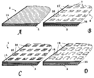
- Figs. lA-lC schematically illustrates the preparations of the
inner and the top (external) current collectors of the
bipolar energy storage device stack of the inventiori;
- Figs. 2A-2D schematically illustrates the preparations of the
separators of the bipolar energy storage device of the
invention;
- Figs. 3A-3B are flowcharts illustrating the process of
preparation of the current collectors and the separators, and
the stacking of the same in a bipolar construction;
- Fig. 4 schematically illustrates construction of a bipolar
energy storage device comprising n cells;
- Fig. 5 schematically illustrates a structure comprising a
plurality of energy storage devices each of which comprising
electrochemical cells; and
- Figs. 6A-6C shows a single cell capacitor product and a
multiple parallel and serial cell capacitor products.
Detailed Description of Preferred Embodiments
The present invention is directed to a multilayered energy
storage device and to a method of its manufacture. More
particularly, the present invention is directed to a bipolar
capacitor constructed from a stack of n+l current collectors
CA 02616726 2008-01-25
WO 2007/013077 PCT/IL2006/000870
- 8 -
and n separators disposed therebetween, wherein an electrode is
attached to n current collectors and n separators (wherein n is
an integer, n>=1) of the stack.
Current collectors to be used according to the present
invention are made of a conductive material that is chemically
inert to the aqueous electrolyte contained in the electrode.
The current collector may be provided in the form of a metal
foil, such as aluminum foil, plated metal or metal coated with
a protective oxide. Alternatively, the current collector is a
polymeric or a co-polymeric sheet, such as polyethylene or
polytetrafluoroethane (Teflon), rubber or PVC
(polyvinylchloride) loaded with conductive particles such as
carbon black, graphite, metallic or plated metallic particles.
In another embodiment, the current collector has a multilayer
structure comprising alternating layers of suitable polymers,
metal foils and carbon or graphite, or similar combinations.
The thickness of the current collector is preferably in the
range of 10 m to 150 m.
The external current collectors (uppermost and bottommost
current collectors in the multilayered structure) are
preferably made of a metallic foil covered by at least one
corrosion resistant layer (e.g., carbon and/or suitable
conductive polymeric composition) . The surface of the metallic
foil is preferably roughened (e.g., by metal deposition,
sputtering, electronic deposition, or mechanical roughening or
chemical etching) . The term "rough surface" is used throughout
the specification to indicate roughness that is due to small
irregularities of the surface, which are intended to maximize
the contact between the metallic foil and the corrosion
resistant layers applied thereon. The internal current
collectors may be either metallic, or alternatively be made of
CA 02616726 2008-01-25
WO 2007/013077 PCT/IL2006/000870
- 9 -
polymeric sheets or metal sheets coated with polymers, as
described above.
The electrodes may comprise carbon, graphite, carbon nano-
particles, fullerene, hollow graphite tubes, metallic
particles, particles of metal oxides and/or metal salts,
electrically conductive polymers, quinones and their
derivatives, ketone compounds, multivalent oxidation compounds,
clays, intercelation compounds, ceramic oxides, and mixtures
thereof. The electrode may contain aqueous electrolyte (acidic,
alkaline, or neutral), and binders (organic or inorganic), and
other additives. The electrode may be in the form of a foil, a
clothe or a dense powdered structure.
Fig. 3A is a flowchart illustrating the preliminary steps of
preparing the current collectors and the separators for the
bipolar capacitor of the invention, as also schematically
illustrated in Figs. lA-1C and 2A-2D. The process starts in
step 30 wherein n separators 15 are mounted on n liners 5 (Fig.
2A). The separators 15 may be provided by a permeable membrane
(e.g., polyethylene, Polytetrafluoroethylene, olefins,
polyvinylidene fluoride (commercially available as Kynar );
most preferably, the separators are provided by a porous film.
For example, according to one preferred embodiment the mounted
separators 3 are prepared from a 25 micron thick teflon based
material and mounted on a 150 micron thick silicone liners by
means of conventional lamination techniques. The mounting of
the separator medium 15 on the liner is required in order to
prevent the occurrence of folds and/or collapse of the
separator during the further steps of the process.
Next, in step 31, the mounted separators 3 are coated by a
layer of adhesive 16, such that separator 15 is sandwiched
CA 02616726 2008-01-25
WO 2007/013077 PCT/IL2006/000870
- 10 -
between the liner 5 and the adhesive layer 16. Adhesive layer
16 is preferably applied via a template (not shown) for
providing complete coverage of the circumferential area of the
mounted separator 3 by adhesive and for leaving adhesive-free
regions 17 through which separators regions 7 may be accessed
(Fig. 2B). In this way the pores in those regions of the
separator medium 15 to which adhesive layer 16 is applied are
blocked by the adhesive.
This step may be carried out utilizing printing techniques, as
described in WO 03/071563. The adhesive used for coating
separator 15 may be a type of solvent based pressure sensitive
adhesive, UV based pressure sensitive adhesive, UV based heat
activated adhesive, solvent based heat activated' pressure
sensitive adhesive, molten pressure sensitive adhesive, molten
heat activated adhesive, or any other polymer with adhesive
characteristics. For example, the adhesive may be C-70
manufactured by Coates.
According to one preferred embodiment of the invention a 15-30
micron thick layer of adhesive is applied to an 120X105 mm
mounted separator 3 via a suitable template by means of screen-
printing for providing 7 rows and 8 columns of (e.g.,
rectangular) adhesive-free regions 17 of a bout 6-100 mmz. The
coated separator 4 is then dried of the adhesive solvent. The
drying may be carried out, for example, by passing it through a
common heat drying tunnel, or any other drying process, such as
a static or a convection drying processes, at room temperature
or at elevated temperature. Step 31 may be repeated if
additional adhesive layers are needed in order to achieve a
thicker layer of adhesive 16 on the coated separator 4.
CA 02616726 2008-01-25
WO 2007/013077 PCT/IL2006/000870
- 11 -
In step 32 a water based polymer 18 (Fig. 2C) is applied to the
adhesive-free regions 17 of the coated separator 4. The water
based polymer 18 provides improved shelf life to the final
product. The water based polymer 18 may be a single blend or
multi-blend of water based polymers, such as PVA (polyvinyl
alcohol), PAA (polyacrylic acid), PEO (polyethylene oxide), PEI
(polyethylene imide), imidazole, or other water based polymer
or copolymer. The vehicle used to carry the water soluble
polymer may further include organic or inorganic additives,
such as surfactants and thickeners. The solution used in this
step may be water based or a composition of water and organic
solution or even organic solutions such as ethanol, isopropanol
or a combination thereof. The water based polymer 18 may be
applied by means of screen-printing. Preferably, a layer of 10-
30 micron thick of water based polymer 18 is printed into the
adhesive-free regions 17, thereby filling the pores of the
accessible separator regions 7. If needed, the applied water
based polymer 18 is dried, for example, by passing it through a
common heat drying tunnel or any other drying process, such as
a static or a convection drying. processes, at room temperature
or at elevated temperature. This step (32) may be repeated, if
needed, in order to provide additional polymer composition 18
in the pores of the accessible separator regions 7.
Next, or concurrently to steps 30-32, in step 33 the surface 9
of one of the sides of each current collector 10 is coated by a
layer of adhesive 11 (Figs. 1A and 1B) . Adhesive layer 11 is
preferably applied via a template (not shown) for providing
complete coverage of the circumferential area of the current
collector 10 by adhesive and for leaving adhesive-free regions
12 through which current collector regions 2 may be accessed
(Fig. 1B). The location and area of the adhesive-free regions
12 of the coated current collector 6 substantially corresponds
CA 02616726 2008-01-25
WO 2007/013077 PCT/IL2006/000870
- 12 -
to the location and area of the adhesive-free regions 17 of the
coated separator 4.
Similarly, this step may be carried out utilizing common
printing techniques. The adhesive used for coating current
collector 10 may be a type of solvent based pressure sensitive
adhesive, UV based pressure sensitive adhesive, UV based heat
activated adhesive, solvent based heat activated pressure
sensitive adhesive, molten pressure sensitive adhesive, molten
heat activated adhesive, or any other polymer with adhesive
characteristics. For example, the adhesive may be C-70 by
coates.
The separator mediums 15 and the current collectors 10 are
substantially of the same spatial dimensions.
For example, in one preferred embodiment of the invention the
external current collectors are manufactured from a 4-100
micron metallic foil.
Each of the external current collectors may be manufactured
from a different material, and the width of one, or both,
external current collector(s) may be thicker than the width of
the internal current collectors. Alternatively or additionally,
the inner side (i.e., the side facing a separator medium) of at
least one of the external current collector, manufactured from
any suitable electrically conductive material such as discussed
above, may be covered with one or more materials for rendering
its surface more resistant to the seepage of the electrolyte.
For example, the inner side of the external current
collector(s) may be covered by a non-metallic yet conductive
polymer material (e.g., BaytronQ) or titanium oxide.
CA 02616726 2008-01-25
WO 2007/013077 PCT/IL2006/000870
- 13 -
The internal current collectors (e.g., 45-2 in Fig. 4) may be
manufactured from carbon and polymer plates, or from a suitable
corrosion durable metallic foil. Most preferably the external
current collectors are in the form of a metallic foil of about
6-20 microns thickness, made of copper, nickel or nickel-
coated copper (which are commercially available), covered by
one or more corrosion resistant layers (made of carbon and/or
suitable polymeric compositions), the thickness of said
layer(s) being in the range of 30-150 micron; preferably a
layer of about 100 micron thickness is applied onto said foil.
The corrosion resistant layer may be attached to the metallic
foil via a corrosion resistant electrically conducting adhesive
layer (e.g., 5-40 micron). The surface of the metallic foil is
preferably roughened in order to maximize the contact between
the corrosion resistant layer and the surface of the metallic
foil. The roughening of the metallic foil surface may be
obtained for example by metal deposition, sputtering,
electronic deposition, or mechanical roughening or chemical or
etching.
According to one preferred embodiment of the invention a 15-30
microns thick layer of adhesive is applied to an -10.5x15 mm
current collector 10 with thickness of about 30-70 micron, via
a suitable template by means of screen-printing for providing
12 rows and 12 columns of (e.g., rectangular) adhesive-free
regions 12 of a bout 10x10 mm. The coated current collector 6
is then dried of the adhesive solvent. The drying may be
carried out, for example, by passing it through a common heat
drying tunnel, or any other drying process, such as a static or
a convection drying process, at room temperature or at elevated
temperature. This step (33) may be repeated if additional
adhesive layers are needed in order to achieve a thicker layer
of adhesive 11 on the coated current collector 6.
CA 02616726 2008-01-25
WO 2007/013077 PCT/IL2006/000870
- 14 -
Fig. 3B is a flowchart demonstrating the steps of constructing
an energy storage device according to the invention, as also
demonstrated in Fig. 4. The first layer of the stack is placed
in step 34, wherein the bottom layer of the stack 45-1 (Fig.
4), an external current collector, is placed such that its
coated surface 9 is directed upwardly. In step 35 electrodes 19
(Fig. 2D) are applied to the adhesive-free regions 17 of the
coated separator 4. Electrodes 19 may be prepared utilizing
conventional suitable electrode compositions, for example the
carbon based compositions described in WO 03/071563 (which
contain an aqueous electrolyte) and they are preferably applied
via a suitable mesh No. 40-200 (e.g., such as, but not limited
to, stainless steal mesh, coated stainless steal mesh, or
polyester mesh) utilizing screen-printing techniques,' or other
techniques, such as stencil techniques. Such a mesh may be
developed using suitable photo emulsion or other masking
techniques, using as known by skilled in the art.
Preparation of a separator layer 46 is completed after applying
electrodes 19 to the coated separator 4. In step 36 blotting,
or other drying process, is (optionally) performed, wherein the
electrodes are compressed and excess electrolyte is absorbed by
an absorbent material. For example, a blotting material (not
shown) is placed above electrodes 19 and a pressure is applied
by a blotting method in order to remove the excess electrolyte
which is absorbed in the blotting material. The blotting
material is then removed from electrodes 19 and discarded. In
step 37 the separator (e.g., separator 46-1 of the first cell
48-1) is 'placed on the stack such that the side containing
electrodes 19 covers the upper side of the previously placed
current collector (e.g., 45-1). The separator 46 is then
attached to the current collector 45, for example, by welding
them together at elevated temperature and pressure, at partial
CA 02616726 2008-01-25
WO 2007/013077 PCT/IL2006/000870
- 15 -
vacuum, or full vacuum. Welding may be performed via heat
welding of the layers or impulse heat welding or other welding
techniques. After attaching the separator 46 to the current
collector 45 the liner 5 is removed from the upper side of the
separator.
If it is determined in step 38 that the last separator layer
(46-n) was placed in the stack in the previous step (37), then
the process is finalized by carrying out steps 42-44. In step
42 electrodes 13 (Fig. 1C) are applied to the adhesive-free
regions 12 of the coated current collector 6. Electrodes 13
preferably comprise the same ingredients as in electrodes 19,
and they are preferably applied via a suitable mesh as in step
35. Preparation of the topmost (external) current collector 45-
(n+1) is completed after performing the (optional) blotting (or
drying) step 43, wherein excess electrolyte is absorbed under
pressure into a blotting material (not shown), as in step 36
above. Finally, in step 44, the topmost current collector 45-
(n+1) is placed on the last separator layer 46-n in the stack,
such that the side of the topmost current collector 45-(n+1)
containing the electrodes 13 covers the upper side of the
previously placed separator layer 46-n.
The topmost current collector 45-(n+1) is then attached to the
previously placed separator layer 46-n, for example, by welding
them together at elevated temperature and pressure, at partial
vacuum, or full vacuum. Welding may be performed via heat
welding of the layers or impulse heat welding or other welding
techniques.
If it is determined in step 38 that additional cell layers
should be added to the stack an internal current collector is
prepared and placed in steps 39-41 and a new cell is then added
CA 02616726 2008-01-25
WO 2007/013077 PCT/IL2006/000870
- 16 -
by transferring the control to step 35. Preparation of the
internal current collector (e.g., 45-2) includes applying
electrodes 13 (step 39) to the adhesive-free regions 12 of a
coated current collector 6, removing excess electrolyte in the
(optional) blotting or drying step 40, and in step 41
connecting the internal current collector to the previously
placed separator (e.g., 46-1) such that the side of the current
collector containing the electrodes 13 covers the upper side of
the previously placed separator layer. The internal current
collector is then attached to the previously placed separator
layer, for example, by welding them together at elevated
temperature and pressure, at partial vacuum, or full vacuum.
Welding may be performed via heat welding of the layers or
impulse heat welding or other welding techniques.
Fig. 5 shows a multilayer construction of a stack 55 comprising
numerous energy storage devices 50. In this example each energy
storage device 50 is comprised of 5 cells (n = 5), 48-1, 48-
2,...,48-5. The width w of such a stack 55 when using 10-30
micron thick separator mediums=15 coated with a layer of glue
of about 50-90 microns, and a 40-70 microns thick current
collectors, coated with a layer of glue of about 5-40 micron,
is about 1-1.2 mm. As exemplified above, this multilayer
construction comprises 5 separators and 4 internal current
collectors, each of which comprises electrodes, and 2 external
current collectors, wherein only the topmost external current
collector comprises electrodes. The energy storage devices 50
may be easily cut out of stack 55 by a scissors or a knife or
other instrument.
It is of course possible to construct a similar multilayer
stack wherein electrodes are also disposed on the external
current collector at the bottom of the stack. In this case the
CA 02616726 2008-01-25
WO 2007/013077 PCT/IL2006/000870
- 17 -
separator placed on top of the external current collector at
the bottom of the stack may be prepared and placed without
carrying step 35, namely without applying electrodes to its
adhesive-free regions.
Fig. 6A shows a single cell capacitor product 60. Capacitor 60
comprises a multilayered energy storage device 50 and two wire
or flat cable leads 61 which are attached to the external
current collectors of the multilayered energy storage device
50, preferably by welding or by utilizing conductive epoxy
glue. Fig. 6B shows and an m-cell capacitor product 62, wherein
a stack of m multilayered energy storage devices, 50-1, 50-2,
50-3,... 50-m, are stacked in series to form a parallel capacitor
product 62. In the parallel capacitor product 62 lead wires 61
are attached to the (bottom) external current collector of the
multilayered energy storage device 50-1 and to the (top)
external current collector of the multilayered energy storage
device 50-m.
Fig. 6C shows and an m-cell capacitor product 66, wherein m
multilayered energy storage devices, 50-1, 50-2, 50-3,... 50-m,
are connected in series to form a serial capacitor product 66.
As shown, m-1 conducting mediums 65 (e.g., metallic foil)
serially connects multilayered energy storage devices, 50-1,
50-2, 50-3,... 50-m, and lead wires 61 to current collectors of
multilayered energy storage devices 50-1 and 50-m.
All of the abovementioned parameters are given by way of
example only, and may be changed in accordance with the
differing requirements of the various embodiments of the
present invention. Thus, the abovementioned parameters should
not be construed as limiting the scope of the present invention
in any way.
CA 02616726 2008-01-25
WO 2007/013077 PCT/IL2006/000870
- 18 -
The above examples and description have of course been provided
only for the purpose of illustration, and are not intended to
limit the invention in any way. As will be appreciated by the
skilled person, the invention can be carried out in a great
variety of ways, employing more than one technique from those
described above, all without exceeding the scope of the
invention.