Note : Les descriptions sont présentées dans la langue officielle dans laquelle elles ont été soumises.
CA 02626345 2008-04-17
WO 2007/048052 PCT/US2006/041355
SYSTEMS AND METHODS FOR RECEIVING AND MANAGING POWER IN
WIRELESS DEVICES
RELATED APPLICATIONS
[0001] This application claims priority to US Provisional Patent Application
Serial Number 60/729,378 filed October 21, 2005, and US Provisional Patent
Application Serial Number 60/760,040, filed January 17, 2006, both
incorporated
herein by reference.
BACKGROUND
[0002] Sensors and traismitters that are small and require low levels of power
for operation are frequently used for collecting information without being
intrusive to
their operating environment. For example, a battery powered sensing and
transmitting
device may be surgically implanted witliin living tissue to sense and transmit
characteristics of the body in which it is implanted.
[0003] The lifetime of the battery used witllin such a sensor often requires
additional surgical procedures to periodically replace the battery. Similarly,
where a
sensor and transmitting device is located within controlled or hazardous
environments, it is often a time-consuming and expensive task to periodically
replace
the battery.
[0004] Energy may be harvested from radio frequency ("RF") waves for use
in remote sensors and transmitting devices. One example of this functionality
is an RF
identification ("RFID") tag that derives power from an RF wave (e.g., from a
transmitting device operating to read the RFID tag) and uses that power to
transmit an
identification signal. One drawback of this technology is that the RFID tags
typically
only operate over short distances.
[0005] A rectenna is an antenna that includes a rectifier; the rectenna
receives
RF waves, rectifies the waves and produces direct current ("DC") electricity.
The DC
electricity produced by the rectenna is dependent on rectenna design, RF wave
frequency, RF wave polarization and RF wave power level incident at the
rectenna.
Typically, the DC electricity output from the rectemza is conditioned by
conditioning
1
CA 02626345 2008-04-17
WO 2007/048052 PCT/US2006/041355
electronics before being fed to a powered device (e.g., sensor,
microprocessor,
transmitter etc.). Where characteristics of the RF wave vary, the DC
electricity output
from the rectenna also varies; this affects power conversion efficiency due to
loading
upoii the rectenna by the conditioning electronics which attempts to maintain
a
constant power output for the powered device.
SUMMARY
[0006] In one embodiment, a radio frequency (RF) reception device has a first
periodic or aperiodic antenna array with one or more antenna elements.
Electrical
conductors provide corniectivity of the antenna elements sucli that selective
reception
of radio frequency energy by the first periodic or aperiodic antenna array is
determined by size and layout of each of the antenna elements, the
connectivity, and
coupling to one or more rectifiers.
[0007] In another embodiment, a reconfigurable radio frequency (RF)
reception device has a plurality of antenna elements, each of the antenna
elements
having at least one rectifier, wherein a first set of antenna elements,
selected from the
plurality of antenna elements, has a first size and wherein a second set of
antenna
elements, selected from the plurality of antenna elements, has a second size.
Electrical
conductors provide connectivity to each of the plurality of antenna elements
and
rectifiers such that selective reception of RF energy by the plurality of
antenna
elements is determined by size, shape, layout and substrate characteristics of
the
plurality of antenna eleinents, the connectivity, and coupling of one or more
rectifiers
to the plurality of antenna elements.
[0008] In another embodiment, a system for selective radio frequency (RF)
reception has a periodic or aperiodic antenna array with a plurality of first
antenna
elements. Electrical conductors provide connectivity to each of the first and
second
sets of antenna elements such that selective polarized reception of RF energy
by the
aperiodic antenna array is determined by orientation and feed points of the
antenna
eleinents, the connectivity, and coupling of one or more rectifiers to each
anteiuia
element.
[0009] In another embodiment, a system collects and conditions variable DC
electrical power fioin at least one source. The system includes conditioning
2
CA 02626345 2008-04-17
WO 2007/048052 PCT/US2006/041355
electronics for converting the variable DC electrical power to storable DC
electricity,
the conditioning electronics presenting a desired impedance to the at least
one source,
and a storage device for storing the storable DC electricity.
[0010] In another enibodiment, a system harvests energy from radio frequency
(RF)/microwave/millimeter-wave power. The system includes a receiving device
witll
at least one antenna and at least one rectifier, the receiving device
converting the
RF/microwave/millimeter-wave power into direct current (DC) electricity. The
system also has a power management unit that (a) configures the receiving
device
based upon the DC electricity, (b) presents a desired load to the receiving
device and
(c) stores the DC electricity.
[0011] hZ another embodiment, a method converts radio frequency (RF)
energy into usable direct current (DC) electricity, including the steps of:
receiving the '
RF energy using at least one rectenna, loading the at least one rectenna with
a desired
impedance, transferring the received power to a storage device, and
conditioning the
stored power to provide the DC electricity.
[0012] In another embodiment, a method converts variable low power DC
electricity into usable direct current (DC) electricity, including the steps
of: sensing
characteristics of the variable low power DC electricity; selecting, based
upon the
sensed characteristics, a DC to DC converter module and operating
characteristics to
convert the variable low power DC electricity to electricity suitable for
storage;
storing the converted electricity in a suitable storage device; and
conditioning the
stored electricity to produce usable DC electricity.
[0013] In another embodiment, a software product has instructions, stored on
computer-readable media, wherein the instructions, when executed by a
computer,
perform steps for designing a system for harvesting energy from RF waves,
including
steps of: interacting with rectenna design software to select desired rectenna
configuration for overall combined rectenna and power manager efficiency;
solving
appropriate converter topology; selecting converter components and operating
conditions for maximum efficiency based upon selected rectemla configuration
and
output characteristics over designated incident power characteristics; and
selecting
appropriate control approach and settings for inaximuin overall system
efficiency over
given system characteristics.
3
CA 02626345 2008-04-17
WO 2007/048052 PCT/US2006/041355
[0014] In another embodiment, a method designs a rectemla, including the
steps of: selecting element size of the rectenna based upon available area,
incident
radiation power levels and operating frequency range; selecting element
polarization
based upon the RF environment of operation; selecting rectenna material based
upon
propagation medium and frequency range; selecting rectenna array shape and
size
based upon required output power levels, available power storage, operational
duty
cycles and available space; selecting a nuniber of elements connected to each
rectifier
based upon incident power levels and selected element size; and selecting a
radome
appropriate for intended use.
[0015] In another embodiment, a software product has instructions, stored on
computer-readable media, wherein the instructions, when executed by a
computer,
perform steps for designing a rectenna, including instructions for:
interactively using
power management design software to select optimum rectenna configuration for
overall combined rectenna and power managenient efficiency; optimizing
rectifier
circuitry based upon application; solving rectifier circuit topology based
upon
optimized rectifier circuitry; solving antenna topology based upon optimized
rectifier
circuitry, polarization, incident radiation power level and frequency using
full-wave
electromagnetic simulations; solving DC network at RF fi=equencies using a
combination of full-wave electromagnetic and high-frequency circuit
simulations;
selecting appropriate combined antenna and rectifier topology; selecting
appropriate
DC network topology and operating characteristics; selecting appropriate array
configuration; and selecting appropriate package for integration with power
manager
based upon siinulation of package for RF compatibility.
[0016] In another embodiment, a software product has instructions, stored on
computer-readable media, wherein the instructions, when executed by a
computer,
perform steps for designing a system for harvesting energy from power sources,
including instructions for: interacting with power source design software to
select one
or more desired power sources for overall combined power source and power
manager efficiency; solving appropriate converter topology; selecting
converter
components and operating conditions for maximum efficiency based upon selected
power source configuration and output characteristics over designated incident
power
characteristics; and selecting appropriate control approach and settings for
maximtun
4
CA 02626345 2008-04-17
WO 2007/048052 PCT/US2006/041355
overall system efficiency over given system characteristics.
[0017] In another embodiment, a software product has instructions, stored on
computer-readable media, wherein the instructions, when executed by a
computer,
perform steps for designing a power source, including instructions for:
interactively
interacting with power management design software to select optimum power
source
configuration for overall combined power source and power management
efficiency;
optimizing power source circuitry based upon application; selecting
appropriate DC
network topology and operating characteristics; and selecting appropriate
package for
integration with power manager based upon simulation of package for power
source
compatibility.
[0018] In another embodiment, a system collects and conditions variable DC
electrical power from at least one source. Conditioning electronics converts
the
variable DC electrical power to storable DC electricity and presents a
positive
resistance load to the at least one source. A storage device stores the
storable DC
electricity. The positive resistance load corresponds to optimal load
resistance of the
source over a range of input power levels.
[0019] In another embodiment, an integrated converter collects and conditions
variable DC electrical power from at least one source. Conditioning
electronics
converts the variable DC electrical power to storable DC electricity and
presents a
positive resistance load to the at least one source. A controller controls the
topology
and switching fi=equency of the conditioning electronics. A storage device
stores the
storable DC electricity. The controller adaptively adjusts one or more of the
switching
frequency and topology to extract power from the rectenna while storing the
harvested
energy.
BRIEF DESCRIPTION OF THE FIGURES
[0020] FIG. 1 shows one embodiment of a power harvesting system that
includes power sources and a controlled iinpedance, voltage or current power
controller.
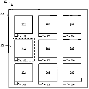
[0021] FIG. 2 shows one exemplary periodic and uniform rectenna array.
[0022] FIG. 3 shows one exemplary aperiodic and non-uniform rectenna
array.
5
CA 02626345 2008-04-17
WO 2007/048052 PCT/US2006/041355
[0023] FIG. 4 illustrates exemplary energy coupling including a plurality of
DC-to-DC converters.
[0024] FIG. 5 is a flowchart illustrating one exemplary process for converting
variable power DC electricity into usable DC electricity.
[0025] FIG. 6 is a flowchart illustrating one process for designing a system
for
harvesting energy from a power source.
[0026] FIG. 7 is a flowchart illustrating one process for designing a
recteima.
[0027] FIG. 8 is a flowchart illustrating another exemplary process for
designing a rectenna.
[0028] FIG. 9 is a flowchart illustrating one exemplary process for designing
a
system for harvesting energy from power sources.
[0029] FIG. 10 shows one exemplary block diagram of one exemplary
rectenna and sensor system embodiment.
[0030] FIG. 11 shows an exemplary model and a layout of a rectenna.
[0031] FIG. 12 shows an exemplary graph illustrating simulated and measured
output power of the rectenna of FIG. 11 as a function of output resistance,
and an
exemplary graph illustrating siinulated and measured output voltage of the
rectenna of
FIG. 11 as a function of output resistance.
[0032] FIG. 13 shows a block diagram illustrating one exemplary DC power
processing circuit for obtaining plus and minus 15V power.
[0033] FIG. 14 shows one exemplary graph illustrating measured DC output
power of the circuit of FIG. 13 against polarization angle of radiation
incident on the
rectenna array and one exemplary graph illustrating DC output power and
efficiency
of the circuit of FIG. 13 against power received by the rectenna array
[0034] FIG. 15 shows one exemplary circuit for a boost converter in variable
frequency critical conduction mode (CRM).
[0035] FIG. 16 shows one exeinplary circuit for a buck-boost converter in
fixed frequency discontinuous conduction mode (DCM).
[0036] FIG. 17 shows two exemplary waveforms illustrating operation of the
converter circuit of FIG. 15.
[0037] FIG. 18 shows one exemplary circuit for generating the gate driving
signals for the circuit of FIG. 15.
6
CA 02626345 2008-04-17
WO 2007/048052 PCT/US2006/041355
[0038] FIG. 19 shows two exemplary equations that define operation of the
circuit of FIG. 15.
[0039] FIG. 20 shows one exemplary two-stage adaptable switching-capacitor
topology of one embodiment.
DETAILED DESCRIPTION OF THE FIGURES
[0040] FIG. 1 shows an embodiment of a power harvesting system 100 that
includes power sources 102 and a controlled impedance, voltage or current
power
controller 104. Power harvesting system 100 is illustratively shown powering a
powered device 106. Powered device 106 is, for example, a sensor and/or
transceiver
device. Power source 102 may represent one or more of: a recteima, a
photovoltaic
cell, a piezoelectric device or other power collecting device.
[0041] Power controller 104 is illustratively shown with energy storage 108,
energy coupling 110 and energy managenlent 112. Energy storage 108 is for
example
a battery or a capacitor; it may be internal to power controller 104, as
shown, or
external to power controller 104 without departing from the scope hereof.
[0042] Energy management 112 instructs energy coupling 110 to convert
energy received from power source 102 into a form suitable for storage by
energy
storage 108. Accordingly, energy coupling 110 may include a DC-to-DC voltage
converter 116 that changes the DC voltage received from power source 102 such
that
it is suitable for storage in energy storage 108. The DC-to-DC voltage
converter 116
may represent a step-up voltage converter or a step down voltage converter.
Or, DC-
to-DC voltage converter 116 may include a plurality of different types of DC-
to-DC
voltage converters that are selectively chosen to convert DC electricity
received from
power source 102 into a fonn suitable for storage by energy storage 102.
[0043] Energy coupling 110 is further shown with optional DC combining
circuit 114, which operates to combine DC inputs from power source 102 where
multiple power sources 102 provide power to controlled iinpedance power
controller
104. DC coinbining circuit 114 may include one or more switches selected by
energy
management 112 to configure connectivity of multiple power sources 102. For
example, where power source 102 is a rectenna array (e.g., rectenna array 200,
FIG.
2) that has a plurality of antenna elements (e.g., antenna elements 202 ),
depending on
7
CA 02626345 2008-04-17
WO 2007/048052 PCT/US2006/041355
sensed characteristics of received power from the aperiodic rectenna, energy
management 112 may control DC coupling circuit 114 to configure antenna
elements
in series and/or parallel for optimum operation. In particular, as power
levels,
frequencies and polarizations of incident RF waves change, energy management
112
may reconfigure connectivity of the rectenna array to improve energy
harvesting
efficiency.
[0044] Energy management 112 may also receive infoi7nation from powered
device 106 via signal 118 that indicates power requirements of powered device
106.
This information is used by energy management 112 to optimally configure
energy
coupling 110.
[0045] In the following examples, power source 102 is represented by one or
more rectennas. However, other power sources may also be used in place of the
rectennas shown.
[0046] FIG. 2 shows one exemplary periodic and uniform rectenna array 200,
illustrating nine square patch antenna elements 202 on a grounded substrate
204. Each
antenna element 202 has. a rectifier 206, thereby forming a rectenna 208.
Interconnectivity of periodic rectemia array 200 is not shown for clarity if
illustration.
Size and layout of each antenna element, connectivity of each rectifier
thereto and
substrate characteristics determine the frequency range and polarization of
radio
frequency waves received by rectenna array 200.
[0047] Array 200 may be formed with alternate antenna designs without
departing from the scope hereof. Moreover, additional rectifiers may connect
in
parallel or series to rectifiers 206, also witllout departing from the scope
hereof.
[0048] FIG. 3 shows one exemplary aperiodic and non-uniform rectenna array
300 with five patch antenna elements 302 of a first size formed on a substrate
304,
each antenna element 302 having a rectifier 306 to form a rectenna 312.
Aperiodic
rectenna array 300 also has a patch antenna element 308 of a second size
formed on
substrate 304; antenna eleinent 308 has a rectifier 310 thus forming a
rectenna 314.
Rectenna 312 is designed for receiving radio frequency waves of a first
frequency
range, and rectenna 314 is designed for receiving radio frequency waves of a
second
frequency range. Thus, the aperiodic and non-uniform rectenna array 300 may
receive
radio frequency waves within both the first frequency range and the second
frequency
8
CA 02626345 2008-04-17
WO 2007/048052 PCT/US2006/041355
range.
[0049] Additional or different rectennas may be included within array 300.
Size, layout and type of each antenna element, connectivity of each rectifier
thereto
determine the frequency range and polarization of radio frequency waves
received by
aperiodic non-uniforin recteima array 300.
[0050] Although not shown in FIGs. 2 and 3, connectivity of rectennas 208
within periodic rectenna array 200 and connectivity of rectennas 312 and 314
within
aperiodic rectenna array 300 may-be based upon radio frequency waves incident
at
each rectemia array and the desired power output of the rectenna array. For
example,
rectennas 208 may be connected in series or parallel.
[0051] Selection of a suitable rectifier topology and rectification device,
based
upon frequency range and power levels received, is also important for
efficient
operation of these rectenna arrays.
[0052] Multiple periodic or aperiodic, uniform or non-uniform, rectenna
arrays may be used to harvest RF energy. For example, output from two periodic
rectenna arrays, each having different sized antenna eleinents (i.e., each
receiving RF
waves of different frequency ranges and/or polarizations) may be combined for
conditioning by controlled impedance (or DC input parameter) power controller
104,
FIG. 1.
[0053] A rectenna aiTay (e.g., periodic rectenna array 200, FIG. 2) may also
be reconfigured during operation. For example, if energy management 112
determines
that output of rectenna- array 200 is low, energy management 112 instructs
energy
coupling 110 to modify comlectivity of rectenna array 200 (e.g., using DC
combining
circuit 114) to increase output voltage. DC combining circuit 114 for example
contains switching components (e.g., MOSFETs, BJT, IGBT, relays, etc.) that
allow
dynamic configuration of connectivity to power source 102.
[0054] If energy manageinent 112 deteirnines that output power of the
rectenna array is high, energy management 112 may instruct energy coupling 110
to
reconfigure antenna elements of rectenna array 200 into parallel and/or serial
comiectivity combinations, thereby reducing changing output voltage and
current.
[0055] Connectivity of one or more rectenna arrays is for example based upon
one or more of output voltages, open circuit voltage, short circuit current,
output
9
CA 02626345 2008-04-17
WO 2007/048052 PCT/US2006/041355
current and output power of one or more anteima elements. Groups of antenna
elements producing similar currents may be connected in serial, whereas groups
of
antenna elements producing similar voltages may be connected in parallel.
Operating
parameters of the power controller 104 may also be based upon one or more of
output
voltages, open circuit voltage, short circuit current, output current and
output power
of one or more antenna elements and / or other power sources.
[0056] Controlled impedance power controller 104 may include one or more
sense circuits for monitoring characteristics of input power.
[0057] The rectenna array may be designed such that RF power from two or
more antemia elements are combined before rectification.
[0058] FIGs. 15, 16 and 18, described below, show exemplary circuits for
presenting desired impedance to one or more power sources (e.g., power source
102,
FIG. 1, periodic rectenna array 200, FIG. 2, and aperiodic rectenna array 300,
FIG. 3).
Prior art DC-to-DC converters typically iinplement inverse resistive loading:
as input
power decreases, resistance presented to the input power source is reduced,
thereby
further loading the input source. Controlled impedance power controller 104,
on the
other hand, maintains resistance presented to the input source at a
substantially
constant level, even as input power levels vary. The controlled impedance may
also
be varied based on sensed conditions of the power source to emulate a desired
iinpedance, input voltage or input current in order to improve the energy
harvesting
efficiency, for example by emulating a positive resistance load where
resistance
presented to the source increases as input power decreases.
[0059] Selection of circuitry for power controller 104 depends on the desired
application. Where high efficiency of energy harvesting is required,
additional
circuitry may be included to sense characteristics of the input power, whereas
if the
power source provides ample power, high efficiency may not be necessary,
allowing
simplified circuitry to be used.
[0060] Alternative power sources may be combined for use with an RF power
source 102. For example, an RF wave rectenna array, a mechanical generator and
a
photovoltaic cell may be used as input to coinbining circuit 114 and power
controller
104. Power controller 104 may then dynamically configure these inputs
depending on
sensed input characteristics and/or desired output requirements in order to
improve
CA 02626345 2008-04-17
WO 2007/048052 PCT/US2006/041355
energy harvesting efficiency. In particular, energy sources may be combined in
such a
way as to provide biasing to each other, thereby increasing overall energy
harvesting
efficiency. Optionally, powered device 106 may provide feedback to energy
management 112 to indicate its power needs. Energy management 112 may then
configure power input connectivity as needed to provide the necessary power.
[0061] Power controller 104 may also transfer energy from energy storage 108
to one or more power source 102 outputs in order to increase the overall
energy
harvesting efficiency. For example, energy can be transferred to the DC output
of a
rectenna for improved biasing, resulting in improved energy harvesting
efficiency.
[0062] Where input power conditions vary, DC-to-DC converter 116 may be
selected from a plurality of converters to match the input power
characteristics. FIG. 4
shows one exemplary energy coupling 402 that includes a plurality of DC-to-DC
converters 404 and an optional DC combining circuit 406. DC combining circuit
406
may represent DC combining circuit 114, FIG. 1. Energy coupling 402 may
represent
energy coupling 110, FIG. 1. For example, each of DC-to-DC converters 404 may
represent one of: a four-switch buck-boost converter, a two-switch buck-boost
converter, a boost converter operating in critical-conduction mode, a buck
converter
controlled to regulate input current or voltage as a function of the
corresponding input
voltage or current, and a switched capacitor converter. DC-to-DC converters
404 are
selectable based upon input power characteristics and the type of storage
device used
for energy storage 108. As input power characteristics change, energy
management
112 may select an alternate DC-to-DC converter as needed.
[0063] Where input power conditions vary, energy management 112 may
change the operating cllaracteristics of DC to DC converter 116 to match the
emulated
input impedance of the converter to the desired load of the power source 102.
For
example, based upon one or more of: sensed open circuit voltage of power
source
102, short circuit current of power source 102, operating voltage and current
of power
source 102, and output power of power source 102, characteristics of DC to DC
converter 116 may be adjusted to einulate an appropriate resistance.
[0064] FIG. 5 is a flowchart illustrating one process 500 for converting
variable power DC electricity into usable DC electricity, in accord with an
einbodiment. Process 500 is for exainple performed by controller 104, FIG. 1.
In step
11
CA 02626345 2008-04-17
WO 2007/048052 PCT/US2006/041355
502, process 500 senses characteristics of the variable low power DC
electricity and.
then selects, in step 504, a DC-to-DC converter module and operating
characteristics
based upon the sensed characteristics, to convert the variable power DC
electric into
electricity suitable for storage. In step 506, electricity suitable for
storage is stored.
For exainple, the electricity may be stored in energy storage 108, FIG. 1. The
stored
energy is then conditioned into the usable electricity. For example, the
energy from
energy store 108 is conditioned and provided as DC electricity to powered
device 106.
[0065] FIG. 6 is a flowchart illustrating one process 600 for designing a
system for harvesting energy from a power source. In step 602, process 600
interacts
with power source design software to select a power source configuration. In
step
604, process 600 solves the appropriate converter topology. In step 606,
process 600
selects the converter components and operating conditions. In step 608,
process 600
selects the appropriate control approach and settings.
[0066] FIG. 7 is a flowchart illustrating one process 700 for designing a
rectenna. In step 702, process 700 selects the element size of the rectenna
based upon
available area, incident radiation power levels and operating frequency range.
In step
704, process 700 selects element polarization based upon the RF enviroiunent
of
operation. In step 706, process 700 selects rectenna material based upon
propagation
medium and frequency range. In step 708, process 700 selects a shape and size
for the
rectenna array based upon required output power levels, available power
storage,
operational duty cycles and available space. In step 710, process 700 selects
a radome
appropriate for intended use.
[0067] FIG. 8 is a flowchart illustrating another exemplary process 800 for
designing a rectenna. In step 802, process 800 uses power management design
software to interactively select optimum rectenna configuration for overall
combined
rectenna and power management efficiency. In step 804, process 800 optimizes
the
selected rectenna circuitry based upon application. In step 806, process 800
solves
rectifier circuit topology based upon optimized rectifier circuitry. In step
808, process
800 solves antenna topology based upon optimized rectifier circuitry,
polarization,
incident radiation power level and frequency using full-wave electromagnetic
siinulations. In step 810, process 800 solves the DC network at RF frequencies
using a
combination of full-wave electromagnetic and high-frequency circuit
simulations. In
12
CA 02626345 2008-04-17
WO 2007/048052 PCT/US2006/041355
step 812, process 800 selects combined antenna and rectifier topology. In step
814,
process 800 selects appropriate rectenna array configuration. In step 816,
process 800
selects an appropriate package for integration with power manager based upon
simulation of package for RF compatibility.
[0068] FIG. 9 is a flowchart illustrating one process 900 for designing a
system for harvesting energy from power sources. In step 902, process 900
interacts
with power source design software to select one or more desired power sources
for
overall combined power source and power manager efficiency. In step 904,
process
900 solves appropriate converter topology. In step 906, process 900 selects
converter
components and operating conditions for maximum efficiency based upon selected
power source configuration and output characteristics over designated incident
power
characteristics. In step 908, process 90.0 selects an appropriate control
approach and
settings for maximum overall system efficiency over given systenl
characteristics.
[0069] FIG. 10 shows a block diagram of one exemplary rectenna and sensor
system 1000. In particular, system 1000 has a rectenna array 1002, DC power
processing 1004, sensor query electronics 1006, information processing 1008
and a
piezoelectric sensor array 1010. In one example, system 1000 is used to sense
structural failures from fatigue within an aircraft. Rectenna array 1002 is
fonned on a
flexible substrate that may be conformed to a moderate curve of an aircraft.
[0070] FIG. 11 shows an exemplary model 1100 and a layout 1150 of an ADS
rectenna 1101. Model 1100 is shown with an antenna 1102, a diode 1104, an
inductor
1106, a capacitor 1108 and a resistor 1110. As shown in layout 1150, a
commercial
lumped element capacitor 1158 representing capacitor 1108 and a small 0.24mm
diameter wire 1156 representing inductor 1106 provide necessary impedance for
an
output filter of rectenna 1101. Output voltage of rectenna 1101 is measured
across a
variable resistor and the DC power is calculated as V2/R.
[0071] FIG. 12 shows an exemplary graph 1200 illustrating simulated and
measured output power of rectenna 1101 as a function of output resistance, and
an
exemplary graph 1250 illustrating simulated and measured output voltage of
rectenna
1101 as a fiinction of output resistance.
[0072] FIG. 13 shows a block diagram illustrating one exemplary DC power
processing circuit 1300 for obtaining plus and minus 15V power. Circuit 1300
is
13
CA 02626345 2008-04-17
WO 2007/048052 PCT/US2006/041355
powered, for example, by an array of rectenna 1101, FIG. 11, not shown.
[0073] FIG. 14 shows one exemplary graph 1400 illustrating measured DC
output power of circuit 1300 against polarization angle of incident radiation
against
the recteima array and one exemplary graph 1450 illustrating DC output power
and
efficiency of circuit 1300 against received power by the rectenna array.
[0074] FIG. 15 shows one exemplary circuit 1500 for a boost converter in
variable frequency critical conduction mode (CRM). FIG. 16 shows one
exeinplary
circuit 1600 for a buck-boost converter in fixed frequency discontinuous
conduction
mode (DCM). Note that in both circuits 1500 and 1600, a two-switch
implementation
is possible due to the floating input power source. The converter circuits
1500, 1600
may be operated continuously at higher input power levels, or operated in a
pulsed
mode at lower power levels, as shown in waveforms 1700 and 1750 of FIG. 17.
[0075] In particular, wavefonn 1700 of FIG. 17 shows inductor current under
steady-state operation of circuit 1500, FIG. 15. In a first transition of
circuit 1500,
transistor Q1 is turned on and Q2 is turned off during to,,, and thus the
inductor current
ramps up from zero to ipk over that time. After this transition, Qi is turned
off, and Q2
is turned on to move the energy to the load. This second transition lasts
until the
inductor current drops to zero. Wlien this occurs, the first transition is
repeated. The
converter of circuit 1500 runs in this mode for a certain duty cycle, k, of a
low
fiequency period, Tlf. At kTlf, the converter turns off and starts up again at
TIf. By
adjusting k or to,,, the emulated input resistance seen by the source is
changed.
Changing the emulated input resistance to match the optimum rectenna load
maximizes energy harvesting.
[0076] In circuit 1500, the input voltage source is shown as Vg, and the
output energy is stored in an energy storage element such as a capacitor or
micro-
battery. The voltage, VZc,-S, is a sense ppint used by a comparator to find a
zero
crossing of the inductor current. Optionally, the open circuit voltage, Vo',,
or a short
circuit current, Is,, may be used by additional control circuitry to find the
operating
input power level and set k. The gate driving signals, gateõ and gatep, are
essentially
the same signal when the converter is operating in critical conduction mode.
However, both drive their respective MOSFETs off after kT~f; thus gateõ is a
low
voltage signal and gatep is a high voltage signal. Ci and C2 are input and
output filter
14
CA 02626345 2008-04-17
WO 2007/048052 PCT/US2006/041355
capacitors. Diode Q2 may be used to precharge the energy storage element, thus
enabling start-up from zero energy. The control circuitry for this boost
converter
generates the gate driving signals, given the zero crossing point of the
inductor current
and the parameters: to,,, Tlf., and k. This is for example achieved with the
exemplary
circuit 1800 shown in FIG. 18.
[0077] The voltage, VZ,,rs, from the power stage is the positive input into a
comparator with the negative input tied to ground. VZ,,,s is a negative
voltage most of
the time. Detection of a zero-crossing by the comparator triggers a pulse,
from a one-
shot circuit, with width ton. This pulse is passed through two OR-gates and
then to
circuit 1500 as gaten and gatep. A second input into the gatep OR-gate is a
signal from
a low frequency oscillator that is logic high after kTlf. This ensures that
both Q1 and
Q2 are off after that point. The low frequency oscillator operating at period,
Tlf, also
provides the same signal to power off the comparator and one-shot circuitry
when the
converter is not in operation for reduced control power loss and to power them
back
on afterwards.
[0078] As can be seen from equation 1950, FIG. 19, if the boost converter
operates continuously, the emulated resistance Re,nulated is only be dependent
on toõ
since k= 1. This simplifies the control circuitry since only the zero crossing
detecting
comparator and the one-shot are used. However, these circuits are on
continuously,
even at low input power. Implementation of the low frequency duty cycle
control
method allows some of the circuitry to be powered off at times, depending on
the
input power level. Note that peak power tracking components in the control
sample
the open circuit voltage, Vo,,, of the input source when the converter is not
in
operation. These components may also sample the short circuit current, IS,,.
These
values maybe used to adjust k or toõ and thus change Reinulated to be the
optimum
impedance load. If operation at lower power levels is desired, these
additional control
blocks may be implemented.
[0079] Prior art power converters for very low power levels have low
efficiency due to parasitic leakage currents and parasitic capacitance to the
substrate.
These limitations are removed by developing a set of integrated converters for
high
efficiency energy harvesting using an RF process. This process is based on
fully-
depleted silicon-on-insulator (FD-SOI) with a thick upper metal layer for
inductors
CA 02626345 2008-04-17
WO 2007/048052 PCT/US2006/041355
and a high resistivity substrate. The primary advantages in this process for
power
processing are reduced parasitic capacitances, which are up to 1000 times
lower than
in a traditional CMOS silicon process. Such low parasitics facilitate high
efficiency
operation, even at very low power levels and frequencies as high as hundreds
of kHz
(allowing small component sizes). An integrated power converter IC may be
constructed with single and two-stage switched capacitor (SC) circuits, which
have
high efficiency at very low power levels since parasitic capacitance is small.
[0080] FIG. 20 shows one exemplary two-stage SC topology 2000. =On-chip
buffers may be provided for each of the switches (S1-S11) and external control
logic
(e.g., controller 2002) may be used to determine the switching configuration.
Topology 2000 generates eight distinct power conversion ratios from the input
voltage (V;,,) to the output voltage (Vout) for rati.os from one third to
three. The
external control chip adaptively adjusts the switching frequency and topology
to
continuously extract maximum power from .attached rectennas while storing the
haivested energy to the output capacitor (Cstol.age). As the output capacitor
voltage
builds, the converter sequences through topologies to maintain optimal loading
of the
rectenna and high efficiency.
[0081] Changes may be made in the above methods and systems without
departing from the scope hereof. It should thus be noted that the matter
contained in
the above description or shown in the accompanying drawings should be
interpreted
as illustrative and not in a limiting sense. The following claims are intended
to cover
all generic and specific features described herein, as well as all statements
of the
scope of the present method and system, which, as a matter of language, might
be said
to fall there between.
16