Note : Les descriptions sont présentées dans la langue officielle dans laquelle elles ont été soumises.
CA 02626966 2008-03-26
74268-POl OCA
SYSTEM AND METHOD FOR DIGITAL MODULATION
TECHNICAL FIELD
[0001] This disclosure relates generally to digital modulation techniques
and more particularly to systems and methods for power amplification and
transmission.
65151664.1
1
CA 02626966 2008-03-26
74268-POl OCA
BACKGROUND OF THE INVENTION
[0002] The basic function of the digital modulation is the signal power
amplification, i.e. power amplifiers. Power amplifier gain is equal to the
ratio of output
power to input power. There are many types of power amplifiers, and the reason
for so
many types is the trade-off of the performance parameters, like implementation
simplicity, distortion (nonlinear characteristic), power efficiency and filter
requirements.
The ideal choice is to have a two level load driver at the power amplifier
output stage
which provides power efficiency, no distortion, simple filter requirements and
simple
implementation if it can be integrated into a silicon chip. Class D amplifiers
meet the
ideal solution, except that they can be operated only in low frequency, like
high power
audio amplifier up to 20kHz bandwidth. The class D amplifier is built with an
analog
circuitry, so it has high distortion.
100031 Up-converting from baseband to particular carrier frequencies is a
well-known function in a RF transmitter. Traditionally, this is accomplished
by a non-
linear process in which the baseband signal is multiplied by a carrier
frequency signal.
Such conversions use a mixer and oscillator which have nonlinear
characteristics. The
nonlinear characteristic process adds harmonics and other spurious noise. It
is possible
for the harmonics to be filtered out, but the in-band noise would remain with
the signal
as a gradation from the conversion.
[0004] There are two design approaches in up-converting processes: the
single stage and the two stage. The problem with the single stage approach is
the carrier
frequency leaky control, and therefore the single stage approach it is not
commonly used.
The second is the two stage up-converting process, wherein the processing is
first
converted to an intermediate frequency (IF), and then the IF is converted to
the carrier
frequency. This creates more demands on filtering and the choice of IF
frequency for
minimizing the in-band noise than from the two stages of the non-linear
process. When
the non-linearity of the power amplifier is included, the transmitter process
has in-band
noise from three non-linear sources.
[0005] Another problem with such traditional circuits is that each baseband
to carrier frequency conversion (in terms of selected frequencies) requires a
unique
65151664.1
2
CA 02626966 2008-03-26
74268-POl OCA
design in order to avoid the harmonics and other spurious signals that result
from the
specific addition and subtraction of frequencies required to achieve the
desired result.
This problem then causes each product design to be unique every time, and thus
involves
engineering effort for introducing every new product.
65151664.1
3
CA 02626966 2008-03-26
74268-POl OCA
BRIEF SUMMARY OF THE INVENTION
[0006] The present invention is directed to a system and method which
allows for power amplification of an input signal using power amplification
combined by
changing the center frequency with an up-converter to shift a baseband signal
to a signal
at a carrier frequency in the same process. This then provides a digital
implementation
that is power efficient and has little or no linearity issue - technology
suitable for a
silicon chip and broadband operation. In one embodiment, each input sample is
replaced
with a number of sub-samples within the same sample interval, the total weight
of the
sub-samples being equal to the replaced sample. This sample to sub-samples
process
alters the frequency response of the sampled signal and reduces the amplitude
dynamic
range of the load driver, thereby simplifying the filter requirements for
digital to analog
conversion while reducing linearity requirement of the load driver. This
process can be
implemented by digital circuits which results in broadband operation.
[0007] The foregoing has outlined rather broadly the features and technical
advantages of the present invention in order that the detailed description of
the invention
that follows may be better understood. Additional features and advantages of
the
invention will be described hereinafter which form the subject of the claims
of the
invention. It should be appreciated by those skilled in the art that the
conception and
specific embodiment disclosed may be readily utilized as a basis for modifying
or
designing other structures for carrying out the same purposes of the present
invention. It
should also be realized by those skilled in the art that such equivalent
constructions do
not depart from the spirit and scope of the invention as set forth in the
appended claims.
The novel features which are believed to be characteristic of the invention,
both as to its
organization and method of operation, together with further objects and
advantages will
be better understood from the following description when considered in
connection with
the accompanying figures. It is to be expressly understood, however, that each
of the
figures is provided for the purpose of illustration and description only and
is not intended
as a definition of the limits of the present invention.
65151664.1
4
CA 02626966 2008-03-26
74268-P010CA
BRIEF DESCRIPTION OF THE DRAWINGS
[0008] For a more complete understanding of the present invention,
reference is now made to the following descriptions taken in conjunction with
the
accompanying drawing, in which:
[0009] FIGURE 1 illustrates a power amplifier embodiment of a system
using the concepts of the invention;
100101 FIGURE 2 illustrates a transmitter embodiment of a system using
the concepts of the invention;
[0011] FIGURE 3 illustrates a time and frequency relationship of a
sampled signal;
[0012] FIGURE 4 is an illustration of sample and sub-samples relationship
in a sampling interval;
[0013] FIGURE 5 A, 5B, 5C show one example of a sample value
selection chart and the resulting frequency response for an amplifier; and
[0014] FIGURES 6A and 6B show one example of a sample value
selection chart and the resulting frequency response for a transmitter.
65151664.1
CA 02626966 2008-03-26
74268-POl OCA
DETAILED DESCRIPTION OF THE INVENTION
[0015] The power amplification process involves a number of stages. The
first stage is to digitize the input signal, if it is not already digitized.
The second stage is
the sample to sub-sample converter which involves replacing each input sample
by a
sub-samples waveform within the sample interval. The weight of sub-sample
waveform
in each sampling interval is equal to the sampled amplitude level of that
being replaced.
The final stage is the amplification of the pulses which does not require a
linear devices.
The most efficient pulse amplifier is an ON/OFF switch.
[0016] The second embodiment is a single stage carrier frequency up-
conversion using digital circuits. The process is very simple if it coupled
with the first
embodiment. In the words, one can the pulse amplifies to a carrier ON/OFF
amplifies.
[0017] In another embodiment, the carrier frequency is changed for
different application or the same FDM application where the total bandwidth is
partition
into multiple channel with different carrier frequency. This invention can
accommodate
this application by changing the carrier frequency oscillator only. There is
no redesign of
the modulator required. The other requirement is that the ratio of the carrier
frequency to
sampling frequency must be an integer which can be calculated automatically
with a
programmable phase locked loop divider.
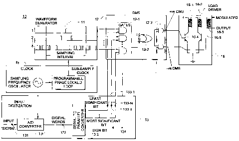
[0018] FIGURE 1 illustrates an embodiment 10 of a system using the
amplifier concepts of the invention. System 10, in the configuration shown, is
a
modulator operable using essentially five digital modules for modulating
baseband input
signal and amplified to drive a load. The five modules are input digitization
13, sub-
sampling waveform generators 11, clocks 15, magnitude control of the
modulating signal
generator 12 and load driver 16.
[0019] Input digitization 13 involves the baseband signal which is in
analog form and is converted to a digital representation by analog to digital
(A/D)
converter 13 operating in the well-known fashion. The conversion is a string
of digital
sample words of N bits(quantized), each word indicating the input signal
amplitude at an
instant of sampling time. The word format is n-1 bits of binary coding for
magnitude
with one bit as the sign bit where N is the total number of bits per sample.
The serial to
65151664.1
6
CA 02626966 2008-03-26
74268-P010CA
parallel conversion is operated on each digital sample word, i.e., all bits in
one word
appear as the outputs at the same time and up-dated at each sample interval.
The size of
N is determined by the noise requirement, sampling frequency and carrier
frequency
fitering requirment.
[0020] The sample to sub-sample conversion function replaces each digital
word by a sub-sample time waveform within each sample interval. This process
is
performed in two stages; the first stage being the sub-sample value waveform
generation
and the second stage being to create the modulated digital signal.
[0021 ] Waveform generators 11 may have outputs from 2 to N-1 based on
a number of possible values per sub-samples. If the output is 2, then the sub-
sample
interval is half of the sample interval. As an example, one output pattern
would be "1" in
the first sub-sample interval and followed by "0". The other output would be
"0"
followed by "1 ". In this context, "1" means a pulse present in the interval
and "0" has
none. Note that the waveforms are orthogonal to each other. As the number of
outputs
increase, the patterns have more choices. For simplicity, the following
description
assumes the number of outputs is N-1, unless otherwise stated. When the number
of
outputs is N-1, then the pattern value could match each digital bit in the
sample word,
i.e., the number of "1" in each output could be 1, 2, 3,... or 2(N"2) . The
waveform
consists of replica unique patterns in each sampling interval. For an example,
the least
significant bit has a value of 1, so the corresponding sub-sample waveform has
a value of
one and replica in every sampling interval and so on. The number of sub-
sampling
intervals in each sampling interval must be greater than or equal to 2(N-1)
due to
orthogonal among the waveforms' requirement as shown in Fig. 4. Examples
provided
in this description use the number of sub-sampling intervals per sampling
interval as 2N
for the same phase shift among waveforms. So the sub-sample waveform of value
of 1
has two pulses evenly spaced on both side of the center line of the sample
interval.
[0022] The choice of unique pattern for each waveform is based on the in-
band and out-of-band frequency responses. The in-band frequency response is
based on
the consistent frequency response for all amplitudes. The out-of-band
frequency
response is based on the out-of-band signal attenuation.
65151664.1
7
CA 02626966 2008-03-26
74268-POl OCA
[0023] FIGURE 5A is a chart illustrating an example of N= 30 or a digital
word of 30 with each sample period having sub-sample intervals. The chart
assumes the
sub-sample values are either 0.5 or 0 in each sub-sample interval. There are
total of 4
sub-sample waveforms with values of 1, 2, 4 and 8 for every sample period. By
adding
one or more waveforms together with a sign bit, the waveform value could from -
15 to
15 in increments of one. This can be done because the waveforms are orthogonal
to each
other.
[0024] FIGURE 5B shows that the normalized frequency response of
waveforms shown in FIGURE 5A is almost identitical up to f 45% of the sampling
frequency. The reason is that the selection of waveform patterns is on the
criteria for a
consistent in-band frequency response for difference sample values. To
represent the
sample value of 1, the placement of sub-sample values are at both sides of the
9I' sub-
sample slot from the center line and so on.
100251 FIGURE 5C shows the normalized frequency response of the sub-
sample waveform from 1 to 15 levels over a wide spectrum range. The
normalization is
based on the peak level, i.e.15. This is another pattern selection for
minimizing the out of
band signals. In this example, 15 dB attenuation over the 1 S' to 3d sampling
frequency
range is acehieved which simplifies the filter requirments.This spectrum
diagram shows
that the digital sample modulated signal has a low pass frequency response at
the
baseband. The original signal can be repoduced after filtering the out of band
signals.
[0026] A digital modulated signal is created (as shown in FIGURE 2) by
combining the outputs of waveform generators 11 and input digitizer 13. Since
outputs
of waveform generators 11 are already based on per bit from input digitizer
13, all that is
required is to "AND" gate (via gates 12-1) each output from waveform
generators 11 and
input digitizer 13 with the same value. For an example, the least significant
bit should
"AND" with the lowest value waveform and so on. The output of the "AND" gate
would
be either a waveform or zero. In other words, if the least significant bit
called for a
waveform, then the output is a value 1 waveform. If not, there is no waveform
or zero
value.The magnitude of the digital modulated signal is the output of "or" gate
12-2 with
all inputs from all the "AND" gates. This magnitude waveform is "AND" (via
gates 12-
65151664.1
8
CA 02626966 2008-03-26
74268-P010CA
3) with a + or - sign bit provided from serial to parallel converter 13-2 to
provide positive
and negative amplitude of the digital modulated signal.
100271 Load driver 16 is the output stage of the amplifier which delivers
the digital modulated signal to the load. It consists of two current paths.
Paths 16-4 and
16-1 deliver positive signal to the load, and paths 16-5 and 16-2 deliver
negative signal
based on the transformer winding direction. Paths 16-4 and 16-5 are on/off
switches
controlled by the digital modulated signal. If there is a pulse to be
transmitted, one
switch would be closed and the other would be open. When there is no pulse for
transmission, both switches would be open. Once the current is flowing in the
transformer, it will transfer the power to secondary winding 16-3 and to the
load. Load
driver 16 is extremely power-efficient which means the power dissipated in the
load
driver is a small percentage of the output power. This results from the
switched
transistors and transformer not dissipating much energy under operation. No
power is
dissipated when the switch is open, and therefore power dissipation is a
percentage of
output power. Hence, nonlinearity is not a problem.
[0028] Clock circuit 15 has two clocks, i.e., sampling and sub-sampling
clocks. The relationship between these two clocks are that the sub-sample
clock is an
integer multiple of the sampling clock. For broadband operation, this clock
circuit
preferably would be a separate module from the silicon integrated chip so that
the chip
can be used for any frequency.
[0029] With respect to the number of waveform generator output ports, the
above discussion is based on N-4 output ports. One disadvantage is the use of
a high sub-
sample clock frequency. By reducing the number of output ports, the sub-sample
clock
frequency would be reduced by half at a time. Referring to FIGURE 5A, let us
assume to
reduce the output port from 4 to 3. The highest waveform value 8 would be
removed.
However, since a preferred result would be to have amplitude of the digital
modulated
signal be the same, e.g., -15 to 15 in increments of one. The following table
shows how
the 151evels will be achieved. The table indicates there are two values of
pulses, i.e. 0.5
and 1. This can be handled by two load drivers where one output is twice the
power of
the other.
65151664.1
9
CA 02626966 2008-03-26
74268-POl OCA
Amplitude Each pulse value of Each pulse value of 1 or 0
value 0.5 or 0
0 No waveform No waveform
1 SV = 1 No waveform
2 No waveform SV = 1
3 SV=1 SV=1
4 No waveform SV=2
SV = 1 SV=2
6 No waveform SV=2 + SV-1
7 SV = 1 SV=2 + SV-1
8 No waveform SV=8
9 SV = 1 SV=8
No waveform SV=8+SV=1
11 SV = 1 SV=8 +SV=1
12 No waveform SV=8+SV=2
13 SV = 1 SV=8+SV=2
14 No waveform SV=8+SV=2+SV=1
SV = 1 SV=8+SV=2+SV=1
[0030] FIGURE 2 shows one embodiment of the concepts discussed herein
being used as a transmitter. Clock circuit 15 is set so that the sub-sample
clock is twice
that of the carrier frequency, each sub-sample clock interval being equal to
the half cycle
of the carrier waveform. For this reason, the choice of sampling frequency is
based on
the carrier frequency. This is different from the amplifier implementation
where the
65151664.1
CA 02626966 2008-03-26
74268-P010CA
sample frequency is the prime determining factor. The major difference between
the
amplifier of FIGURE 1 and the transmitter of FIGURE 6 is that a mixer 14 is
added.
The mixer 14 transforms the baseband signal to a carrier frequency which is
half of the
sub-sample clock frequency.
[00311 Using the sub-sample waveform shown in FIGURE 5A and making
the value in the odd number time slots to be the same and the value in the
even number
time slots to be negative, the result is shown in FIGURE 6A. Converting the
sub-sample
waveform in FIGURE 5A to FIGURE 6A is the function of mixer 14. This function
of
alternating the sign between even and odd time slots is achieved by
effectively
multiplying the signal by a sinusoidal carrier frequency waveform which is the
carrier
modulation function. The implementation consists of mixers 14-1 and 14-2 used
for the
positive DMS and mixers 14-3 and 14-4 for the negative DMS. Mixer 14-1 sorts
out the
odd time slot positive DMS waveform and mixer 14-2 sorts out the even time
slot
positive DMS waveform. This configuration repeats for the negative DMS
waveform, by
mixers 14-3 and 14-4. The "OR" gates 14-5 and 14-6 combine the odd and even
slot
waveforms from the "AND" gates 14-1 and 14-3 and 14-2 and 14-4 respectively.
The
odd time slot output of "OR" gate 14-5 is connected to the positive load
driver while the
even time slot output of "OR" gate 14-6 is connected to the negative load
driver.
[0032] FIGURE 6B shows the normalized frequency response of the sub-
sample waveform from 1 to 15 levels and normalized to the highest level, i.e.
15. One
can see the peak power is a frequency of 15 times the sampling frequency. The
out of
band signal is attenuated by 15 dB over the frequency range of 13 to 14 times
the
sampling frequency.
[0033] An example of designing a mobile CDMA transmitter 900 MHz
system is shown in Chart 1 below. The carrier frequency range is 824 to 836.5
MHz.
The number of channels in the frequency is 10. Channel bandwidth is 1.25 MHz.
65151664.1
11
CA 02626966 2008-03-26
74268-POl OCA
The center carrier frequencies are shown in Chart 1.
Channel # Frequency
1 824.625
2 825.875
3 827.125
4 828.375
829.625
6 830.875
7 832.125
8 833.375
9 834.625
835.875
[0034] From the frequency range, the minimum sampling rate is half the
range, e.g. 6.25 MHz. The number of sub-intervals is 824.625/6.25 - 256. The
sampling
frequency is 6.44238 MHz and carrier frequency is 644238x 128 =824.62446 MHz.
The
signal to noise ratio is equivalent to 9 bits (128 level magnitude + one sign
bit + 1 bit for
over sampling).
65151664.1
12
CA 02626966 2008-03-26
74268-POl OCA
Chart 2 shows the sampling frequencies.
Channel # Sampling Frequencies Carrier Unit
Carrier frequency
error
1 6.44238 824.62464 0.00036 MHz
2 6.45215 825.8752 -0.0002 MHz
3 6.46191 827.12448 0.00052 MHz
4 6.47168 828.37504 0.00004 MHz
6.48145 829.6256 -0.0006 MHz
6 6.49121 830.87488 0.00012 MHz
7 6.50098 832.12544 -0.00044 MHz
8 6.51074 833.37472 0.00028 MHz
9 6.52051 834.62528 -0.00028 MHz
6.53027 835.87456 0.00044 MHz
[0035] FIGURE 4 is an illustration of on embodiment of sub-samples in a
sampling interval. Each sampling interval is divided into M equally spaced sub-
sample
intervals and each sub-sample interval would transmit one sub-sample value.
The
preference is to have two level sub-sample value, e.g. I or 0. However, the
modulation
scheme can support multi-level sub-sample values. The sum of all sub-sample
values
equals the sample value. By using this approach the dynamical range of
circuitries that
are necessary to support the samples is reduced substantially, e.g. by N where
N is the
number of sub sample intervals in one sample period. Note that the
presentation of
sample value has two dimension; namely, the magnitude of the sub-sample values
and
the density of the sub-sample values. This then allows carrier modulated
signal
generation to be performed by digital circuits.
[0036] Note that the input signal can be an analog signal on input 131
(FIGURE 3)or it could be a digital signal or a quantized digital signal on
input 132. In
65151664.1
13
CA 02626966 2008-03-26
74268-PO l OCA
addition, the signal can be serial (as shown at input 132) or parallel (as
shown at
terminals 133-1 to 133-N) in format. The carrier frequency could be built into
the device
or it can be obtained via an input, such as input 130. The sign bit would be
provided via
terminal 134.
100371 Although the present invention and its advantages have been
described in detail, it should be understood that various changes,
substitutions and
alterations can be made herein without departing from the spirit and scope of
the
invention as defined by the appended claims. Moreover, the scope of the
present
application is not intended to be limited to the particular embodiments of the
process,
machine, manufacture, composition of matter, means, methods and steps
described in the
specification. As one of ordinary skill in the art will readily appreciate
from the
disclosure of the present invention, processes, machines, manufacture,
compositions of
matter, means, methods, or steps, presently existing or later to be developed
that perform
substantially the same function or achieve substantially the same result as
the
corresponding embodiments described herein may be utilized according to the
present
invention. Accordingly, the appended claims are intended to include within
their scope
such processes, machines, manufacture, compositions of matter, means, methods,
or
steps.
65151664.1
14