Note : Les descriptions sont présentées dans la langue officielle dans laquelle elles ont été soumises.
CA 02628871 2008-05-07
WO 2007/054928
PCT/11,2006/001278
POLARIZING OPTICAL SYSTEM
Field of the Invention
The present invention relates to substrate-guided optical devices, and more
particularly, to devices which include a plurality of reflecting surfaces
carried by a
common light-transmissive substrate, also referred to as a light-guide.
The invention can be implemented to advantage in a large number of imaging
applications, such as, for example, head-mounted and head-up displays,
cellular
phones, compact displays, 3-D displays, compact beam expanders as well as non-
imaging applications such as flat-panel indicators, compact illuminators and
scanners.
Background of the Invention
One of the important applications for compact optical elements is in head-
mounted displays, wherein an optical module serves both as an imaging lens and
a
combiner, in. which a two-dimensional display is imaged to infinity and
reflected into
the eye of an observer. The display can be obtained directly from either a
spatial
light modulator (SLM), such as a cathode ray tube (CRT), a liquid crystal
display
(LCD), an organic light emitting diode array (OLED), or a scanning source and
similar devices, or indirectly, by means of a relay lens or an optical fiber
bundle. The
display comprises an array of elements (pixels) imaged to infinity by a
collimating
lens and transmitted into the eye of the viewer by means of a reflecting or
partially
reflecting surface acting as a combiner for non-see-through and see-through
applications, respectively. Typically, a conventional, free-space optical
module is
used for these purposes. As the desired field-of-view (FOV) of the system
increases,
such a conventional optical module becomes larger, heavier, bulkier and
therefore,
even for a moderate performance device, impractical. This is a major drawback
for
all kinds of displays, but especially in head-mounted applications, where the
system
must necessarily be as light and as compact, as possible.
The strive for compactness has led to several different complex optical
solutions, all of which, on the one hand, are still not sufficiently compact
for most
practical applications, and, on the other hand, suffer major drawbacks in
terms of
manufacturability. Furthermore, the eye-motion-box (EMB) of the optical
viewing
CA 02628871 2008-05-07
WO 2007/054928 PCT31,2006/001278
2
angles resulting from these designs is usually very small - typically less
than 8 mm.
Hence, the performance of the optical system is very sensitive, even to small
movements of the optical system relative to the eye of the viewer, and does
not allow
sufficient pupil motion for convenient reading of text from such displays.
Disclosure of the Invention'
The present invention facilitates the design and fabrication of very compact
light-guide optical elements (LOB) for, amongst other applications, head-
mounted
displays. The invention allows relatively wide FOVs together with relatively
large
EMB values. The resulting optical system offers a large, high-quality image,
which
also accommodates large movements of the eye. The optical system offered by
the
present invention is particularly advantageous because it is substantially
more
compact than state-of-the-art implementations and yet it can be readily
incorporated
even into optical systems having specialized configurations.
The invention also enables the construction of improved head-up displays
(HUDs). Since the inception of such displays more than three decades ago,
there has
been significant progress in the field. Indeed, HUDs have become popular and
they
now play an important role, not only in most modem combat aircraft, but also
in
civilian aircraft, in which HUD systems have become a key component for low-
visibility landing operation. Furthermore, there have recently been numerous
proposals and designs for HUDs in automotive applications where they can
potentially assist the driver in driving and navigation tasks. Nevertheless,
state-of-
the-art HUDs suffer several significant drawbacks. All HUDs of the current
designs
=
=
require a display source that must be offset a significant distance from the
combiner
to ensure that the source illuminates the entire combiner surface. As a
result, the
= combiner-projector HUD system is necessarily bulky and large, and
requires a
considerable installation space, which makes it inconvenient for installation
and at
times even unsafe to use. The large optical aperture of conventional HUDs also
poses a significant optical design challenge, rendering the HUDs with either
compromised performance, or leading to high cost wherever high-performance is
=
CA 02628871 2008-05-07
WO 2007/054928 PCT/1L2006/001278
3
required. The chromatic dispersion of high-quality holographic HUDs is of
particular
concern.
An important application of the present invention relates to its
implementation
in a compact HUD, which alleviates the aforementioned drawbacks. In the HUD
design of the current invention, the combiner is illuminated with a compact
display
source that can be attached to the substrate. Hence, the overall system is
very
compact and can readily be installed in. a variety of configurations for a
wide range of
applications. In addition, the chromatic dispersion of the display is
negligible and, as
such, can operate with wide spectral sources, including a conventional white-
light
source. In addition, the present invention expands the image so that the
active area of
the combiner can be much larger than the area that is actually illuminated by
the light
source.
A further application of the present invention is to provide a compact display
with a wide FOV for mobile, hand-held application such as cellular phones. In
today's wireless internet-access market, sufficient bandwidth is available for
full
video transmission. The limiting factor remains the quality of the display
within the
device of the end-user. The mobility requirement restricts the physical size
of the
displays, and the result is a direct-display with a poor image viewing
quality. The
present invention enables a physically very compact display with a very large
virtual
image. This is a key feature in mobile communications, and especially for
mobile
internet access, solving one of the main limitations for its practical
implementation.
The present invention thereby enables the viewing of the digital content of a
full
format Internet page within a small, hand-held device, such as a cellular
phone.
The broad object of the present invention, therefore, is to alleviate the
drawbacks of state-of-the-art compact optical display devices and to provide
other
optical components and systems having improved performance, according to
specific
requirements.
The invention therefore provides an optical system, comprising a light-
transmitting substrate having at least two major surfaces parallel to each
other and
edges, and an optical device for coupling light into said substrate by total
internal
CA 02628871 2008-05-07
WO 2007/054928
PC171L2006/001278
4
reflection, characterized in that said device for coupling light includes a
polarization
sensitive reflecting surface.
Brief Description of the Drawings
The invention is described in connection with certain preferred embodiments
with reference to the following illustrative figures, so that it may be more
fully
understood.
With specific reference to the figures in detail, it is stressed that the
particulars
shown are by way of example and for purposes of illustrative discussion of the
preferred embodiments of the present invention only, and are presented in the
cause
of providing what is believed to be the most useful and readily understood
description
of the principles and conceptual aspects of the invention. In this regard, no
attempt is
made to show structural details of the invention in more detail than is
necessary for a
fundamental understanding of the invention. The description taken with the
drawings
are to serve as direction to those skilled in the art as to how the several
forms of the
invention may be embodied in practice.
In the drawings:
Fig. 1 is a side view of a generic form of a prior art folding optical device;
Fig. 2 is a side view of an exemplary light-guide optical element;
Figs. 3A and 3B illustrate the desired reflectance and transmittance
characteristics of
selectively reflecting surfaces for two ranges of incident angles;
Fig. 4 is a schematic sectional-view of a reflective surface embedded inside a
light-guide
optical element;
Fig. 5 illustrates an exemplary embodiment of a light-guide optical element
embedded in
a standard eyeglasses frame;
Fig. 6 illustrates an exemplary embodiment of a light-guide optical element
embedded in
a hand carried display system;
Figs. 7 A to 7D are diagrams illustrating a method for fabricating an array of
partially
reflecting surfa.ces along with a coupling-in reflecting surface;
Fig. 8 is a side view of another exemplary light-guide optical element;
CA 02628871 2008-05-07
WO 2007/054928 PCT/EL2006/001278
Figs. 9 A to FIG. 9D, 10A to 101) and 11A to 11D are diagrams illustrating
other ,
methods for fabricating an array of partially reflecting surfaces along with a
coupling-in reflecting surface;
Fig. 12 is a diagram illustrating a system for coupling-in polarized input
waves into a
light-guide optical element in accordance with the present invention;
Fig. 13 is a side view of an exemplary light-guide optical element in
accordance with the
present invention;
Fig. 14 illustrates two marginal rays coupled into a light-guide optical
element by a
coupling-in conventional reflecting surface;
Fig. 15 illustrates two marginal rays coupled into a light-guide optical
element by a
coupling-in polarization-sensitive reflecting surface, in accordance with the
present invention;
Fig. 16 is a diagram illustrating another embodiment for coupling-in input
waves into a
light-guide optical element, exploiting a collimating lens, in accordance with
the
present invention;
Fig. 17 illustrates two marginal rays coupled into a light-guide optical
element by a
coupling-in polarization-sensitive reflecting surface utilizing a collimating
lens,
in accordance with the present invention;
Fig. 18 is a diagram illustrating a device for collimating and coupling-in
input waves
from a display source into a light-guide optical element, in accordance with
the
present invention;
Fig. 19 is a diagram illustrating another embodiment for collimating and
coupling-in
input waves from a display source into a light-guide optical element, in
accordance with the present invention;
Fig. 20 is a diagram illustrating yet another embodiment for collimating and
coupling-in
input waves from a display source into a light-guide optical element, in
accordance with the present invention, and
Fig. 21 is a diagram illustrating still a further embodiment for coupling-in
unpolarized
input waves into a light-guide optical element, in accordance With the present
invention.
CA 02628871 2008-05-07
WO 2007/054928
PCT/IL2006/001278
6
Detailed Description of Preferred Embodiments
Fig. 1 illustrates a conventional folding optics arrangement, wherein the
substrate 2 is illuminated by a display source 4. The display is collimated by
a
collimating lens 6. The light from the display source 4 is coupled into
substrate 2 by
a first reflecting surface 8 in such a way that the main ray 10 is parallel to
the
substrate plane. A second reflecting surface 12 couples the light out of the
substrate
and into the eye of a viewer 14. Despite the compactness of this
configuration, it
suffers significant drawbacks; in particular, only a very limited FOV can be
affected.
As shown in Fig. 1, the maximum allowed off-axis angle inside the substrate
is:
arctan( T = (I)
a - ,
wherein T is the substrate thickness;
do, is the desired exit-pupil diameter, and
/ is the distance between reflecting surfaces 8 and 12.
With angles higher than aza. the rays are reflected from the substrate surface
before arriving at the reflecting surface 12. Hence, the reflecting surface 12
will be
illuminated at an undesired direction and ghost images appear.
Therefore, the maximum achievable FOV with this configuration is:
FOV, 2vanõ (2)
wherein v is the refractive index of the substrate.
Typically the refractive index values lie in the range of 1.5-1.6.
Commonly, the diameter of the eye pupil is 2 to 6 mm. To accommodate
movement or misalignment of the display, a larger exit-pupil diameter is
necessary.
Taking the minimum desirable value at approximately 8 to 10 mm, the distance
between the optical axis of the eye and the side of the head, 415, typically,
between
40 and 80 mm. Consequently, even for a small FOV of 8 , the desired substrate
thickness would be of the order of 12 mm.
Methods have been proposed to overcome the above problem, including
utilizing a magnifying telescope inside the substrate and non-parallel
coupling
CA 02628871 2008-05-07
WO 2007/054928
PC171L2006/001278
7
directions. Even with these solutions, however, and even if only one
reflecting
surface is considered, the system's thickness rem- ins limited by a similar
value. The
FOV is limited by the diameter of the projection of the reflective surface 12
on the
substrate plane. Mathematically, the maximum achievable FOV, due to this
limitation, is expressed as:
Ttancr.. dey, (3)
FOV ______________________________
Roe
wherein otsur is the angle between the reflecting surface and the normal to
the
substrate plane, and
Reye is the distance between the eye of the viewer and the substrate
(typically,
about 30-40 mm).
Practically tana,õ cannot be much larger than 1; hence, for the same
parameters described above for a FOV of 8 , the required substrate thickness
here is
in the order of 7 mm, which is an improvement on the previous limit.
Nevertheless,
as the desired FOV is increased, the substrate thickness increases rapidly.
For
instance, for desired FOVs of 15 and 300 the substrate limiting thickness is
18 mm
or 25 mm, respectively.
To alleviate the above limitations, it is possible to utilize an array of at
least
one parallel selectively reflecting surface, fabricated within a LOE
comprising a flat
light-transmitting substrate having at least two major surfaces and edges.
Fig. 2
illustrates a sectional view of an LOE. The first reflecting surface 16 is
illuminated
by a collimated light waves 18 emanating from a display source (not shown)
located
behind the device. The reflecting surface 16 reflects the incident light from
the
source such that the light is trapped inside a planar substrate 20 by total
internal
reflection. After several reflections from the surfaces of the substrate, the
trapped
waves reach an array of selectively reflecting surfaces 22, which couple the
light out
of the substrate into the eye of a viewer 24. Assuming that the central wave
of the
source is coupled out of the substrate 20 in a direction normal to the
substrate
surface 26 and the off-axis angle of the coupled wave inside the substrate 20
is ain,
then the angle asõ,2 between the reflecting surfaces and the substrate plane
is:
CA 02628871 2008-05-07
WO 2007/054928
PCT/11,2006/001278
8
(4)
asur2 = -L" =
2
As can be seen in Fig. 2, the trapped rays arrive at the reflecting surfaces
from
two distinct directions 28, 30. In this particular embodiment, the trapped
rays arrive
at the reflecting surface from one of these directions 28 after an even number
of
reflections from the substrate surfaces 26, wherein the incident angle prd
between the
trapped ray and the normal to the reflecting surface is:
aõ, (5)
fire.' = a in " a sur2 = ¨2 =
The trapped rays arrive at the reflecting surface from the second direction 30
after an odd number of reflections from the lower substrate surfaces 26, where
the
off-axis angle is cein 180R-otin and the incident angle between the trapped
ray and
the normal to the reflecting surface is:
nõ,õ 3ain
13' ref= = 180 - ¨ ot..2 lay- ¨ . (6)
2
In order to prevent undesired reflections and ghost images, it is important
that
the reflectance be negligible for one of these two directions. The desired
discrimination between the two incident directions can be achieved if one
angle is
significantly smaller than the other one. It is possible to design a coating
with very
low reflectance at high incident angles and a high reflectance for low
incident angles.
This property can be exploited to prevent undesired reflections and ghost
images by
eliminating the reflectance in one of the two directions. For example choosing
25 from Equations (5) and (6) it can be calculated that:
Pre =105 ; ain= 50 ; a'õ, =130 ; a,õ = 25 . (7)
Now, if a reflecting surface is determined for which (3',.ef is not reflected
but
pref is, the desired condition is achieved. Figs. 3A and 313 illustrate the
desired
reflectance behavior of selectively reflecting surfaces. While the ray 32
(Fig. 3A),
having an off-axis angle of 13,.qf ¨ 25 , is partially reflected and coupled
out of the
CA 02628871 2008-05-07
WO 2007/054928
PCT/1L2006/001278
9
substrate 34, the ray 36 (Fig. 3B), which arrives at an off-axis angle of
f3',.ef ¨ 750 to
the reflecting surface (which is equivalent to (3'ref 105 ), is transmitted
through the
reflecting surface 34, without any notable reflection.
Hence, as long as it can be ensured that ji'ref, where very low reflections
are
desired, will have negligible reflection, similar to that at 13'õ/¨ 750, over
its angular
spectrum, while prey., will have higher reflections, over its angular
spectrum, for a
given FOV, the reflection of only one substrate mode into the eye of the
viewer and a
ghost-free image, can be ensured.
It is important not only to couple the image out of the substrate without any
distortion or ghost image, but also to couple the light properly into the
substrate.
Fig. 4, which illustrates one method for coupling-in, presents a sectional
view of the
reflective surface 16, embedded inside the substrate 20 and couples light 38a,
38b
from a display source (not shown) and traps it inside the substrate 20 by
total internal
reflection. To avoid an image with gaps or stripes, it is essential that the
trapped light
will cover the entire area of the LOE major surfaces. To ensure this, the
points on the
boundary line 41 between the edge of the reflective surface 16 and the upper
surface 40 of the substrate 20, should be illuminated for a single wave by two
different rays that enter the substrate from two different locations: a ray
38a that
illuminates the boundary line 41 directly, and another ray 38b, which is first
reflected
by the reflecting surface 16 and then by the lower surface 42 of the
substrate, before
illuminating the boundary line.
The embodiment described above with regard to Fig. 4 is an example of a
method for coupling input waves into the substrate. Input waves could,
however, also
be coupled into the substrate by other optical means, including (but not
limited to)
folding prisms, fiber optic bundles, diffraction gratings, and other
solutions.
Fig. 5 illustrates an embodiment that utilizes the coupling-in device
described
in Fig. 4, in which the LOE 20 is embedded in an eyeglasses frame 48. The
display
source 4, the collimating lens 6, and the folding lens 50 are assembled inside
the arm
portions 52 of the eyeglasses frame, next to the edge of the LOB 20. For cases
where
the display source is an electronic element, such as a small CRT, LCD or OLED,
the
CA 02628871 2008-05-07
WO 2007/054928 PCT/EL2006/001278
driving electronics 54 for the display source can be assembled inside the back
portion
of the arm 48. A power supply and data interface 56 can be connected to arm 48
by a .
lead 58 or other communication means, including radio or optical transmission.
Alternatively, a battery and miniature data link electronics can be integrated
into the
eyeglasses frame.
Fig. 6 illustrates another application that utilizes the coupling-in
embodiment
described in Fig. 4. This application is a hand-held display (HBD), which
resolves the
previously opposing requirements of achieving small mobile devices, and the
desire
to view digital content on a full format display, by projecting high quality
images
= directly into the eye of the user. An optical module including the
display source 4,
the folding and collimating optics 6 and the substrate 20 is integrated into
the body of
a cellular phone 60, where the substrate 20 replaces the existing protective
cover-
window of the phone. Specifically, the volume of the support components,
including
= source 4 and optics 6 is sufficiently small to fit inside the acceptable
volume for
modern cellular devices. In order to view the full screen trpincmitted by the
device,
the user positions the window in front of his eye 24, observing the image with
high
FOV, a large EMB and a comfortable eye-relief. It is also possible to view the
entire
FOV at a larger eye-relief by tilting the device to display different portions
of the
image. Furthermore, since the optical module can operate in see-through
configuration, a dual operation of the device is possible. That is, there is
an option to
maintain the conventional cellular display 62 intact. In this manner, the
standard,
low-resolution display can be viewed through the LOB 20 when the display
source 4
is shut-off. In a second, virtual-mode, designated for e-mail reading,
interact surfing, =
or video operation, the conventional display 62 is shut-off, while the display
source 6
projects the required wide FOV image into the eye of the viewer through the
LOB 20.
The embodiment described in Fig. 6 is only an example, illustrating that
applications
other than head-mounted displays can be materialized. Other possible hand-
carried
= arrangements include palm computers, small displays embedded into
wristwatches, a
pocket-carried display having the size and weight reminiscent of a credit
card, and
many more.
CA 02628871 2008-05-07
WO 2007/054928
PCT/1L2006/001278
11
As illustrated in Figs. 5 and 6, there is one major difference between the two
applications. In the eyeglasses configuration illustrated in Fig. 5, the input
waves and
the image waves are located on the same side of the substrate, while in the
hand-held
configuration illustrated in Fig. 6, the input and the image waves are located
on
opposite sides of the substrate. This difference not only affects the shape
and size of
the overall opto-mechanical module, but also determines the internal structure
of the
LOE. As illustrated in Fig. 2, wherein the input waves and the image waves are
located on the same side of the substrate, the coupling-in element 16 is
embedded
inside the LOE 20 in a different orientation to that of the couple-out
elements 22. As
illustrated in Figs. 7A to 7D, however, wherein the input and the image waves
are
located on opposite sides of the substrate, the coupling-in element 16 is
embedded
inside the LOE 20 in a similar orientation to that of the couple-out elements
22. In
fact, the reflecting surface 16 is usually parallel to the partially
reflecting surfaces 22.
This difference is not only cosmetic, but also can significantly influence the
fabrication procedure of the LOE.
It is important that the fabrication process of the LOE will be as simple and
inexpensive as possible. Although this is true for all the potential
applications, it is
especially critical for applications wherein the price of the final product
must be
appropriate for the consumer market. Figs. 7A to 7D illustrate a method of
fabricating an LOE with the internal structure illustrated in Fig. 8. First,
as seen in
Fig. 7A, a group of parallel plates 64 and an associated group of partially
reflecting
surfaces (coated onto these plates) are manufactured, to the required
dimensions. The
plates 64 can be fabricated from silicate-based materials such as BK-7 with
the
conventional techniques of grinding and polishing, or alternatively, they can
be made
from polymer or sot-gel materials using injection-molding or casting
techniques.
Next, a blank plate 66, the coated plates 64, and a plate having a reflecting
surface 68
are cemented together to create a stacked form 70, as illustrated in Fig. 7B.
A
segment 72 (see Fig. 7C) is then sliced off the stacked form by cutting,
grinding and
polishing, to create the desired LOE 20, shown in Fig. 7D. The procedure
illustrated
in Figs. 7A to 71) of coating, cementing, slicing, grinding and polishing can
be totally
CA 02628871 2008-05-07
WO 2007/054928
PCT/1L2006/001278
12
automated to devise a straightforward and inexpensive procedure, which would
be
appropriate for mass production processes.
For LOEs having the internal structures of Fig. 2, the fabrication procedure
is
much more complicated. Figs. 9A to 91) illustrate a method of fabricating an
LOB
having the required internal structure. The group of parallel coated plates
64,
Fig. 9A, are manufactured as before, however, since the reflecting surface 16
(Fig. 2)
is no longer parallel to surfaces 22, the plate with the reflecting surface 68
cannot be
cemented to the stack 70 as before. Therefore, the coupling-out portion of the
LOB
only can be fabricated in the above manner, that is, only the blank plate 66
and the
coated plates 64 are cemented together to create the stacked form 74, shown in
Fig. 9B. A segment 76 (Fig. 9C) is then sliced off the stacked form by
cutting,
grinding and polishing, to create the coupling-out portion 78 (Fig. 9D) of the
desired
LOB 20. '
Figs. 10A to 101) illustrate how the coupling-in portion 82 of the LOB is
prepared separately, in the same manner, as follows: another blank plate 79
(Fig. 10A) and the plate 68 having the required reflecting surface are
cemented
together to create a stacked form 80 (Fig. 10B). A segment 81, shown in Fig.
IOC, is
then sliced off the stacked form by cutting, grinding and polishing, to devise
the
desired coupling-in portion 82 (Fig. 10D).
Figs. 11A and 11B illustrate how the final fabrication step of the LOB is
completed. The coupling-out portion 78 and the coupling-in portion 82 are
cemented
together along the common surface 84 to create the final LOB 20. Since, for
most
applications, the quality of the optical surfaces is critical, the final step
of polishing
the outer surfaces 26 and 27, shown advantageously to be added to the process.
There are some disadvantages to the fabrication process illustrated in Figs.
9A
to 91), 10A to 101) and 11A to 11D as compared to the process illustrated in
Figs. 7A
to 7D. Not only that the number of the fabricating steps is increased from one
to
three, but most significantly, the last step is particularly complicated and
requires
special manufacturing attention. The common surface 84 should be fabricated,
with
high accuracy, normal to the major surfaces 26 and 27 in both portions 78 and
82.
CA 02628871 2008-05-07
WO 2007/054928
PCT/1L2006/001278
13
Moreover, the cemented surface 84 might be broken during the final grinding
and
= polishing step, especially for fabrication of very thin substrates.
= Hence, an LOB having an internal structure as illustrated in Fig. 8, is
preferred
over that of Fig. 2. It is therefore important to find a method to fabricate
an LOE
having the former configuration even for optical systems wherein the input
waves and
the image waves are located on the same side of the substrate. A method which
achieves these two seemingly contradictory requirements and which exploits the
fact
that in most micro-display sources, such as LCD or LCOS, the light is linearly
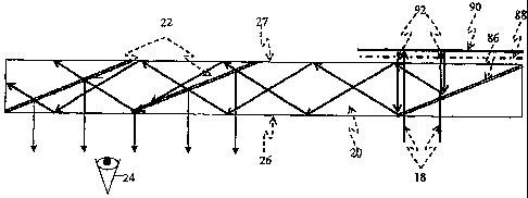
polarized, as illustrated in Fig. 12. The main difference between the
embodiment
illustrated here and the embodiment illustrated in Figs. 2 and 8 is that
instead of
utilizing a uniformly reflecting mirror 16 as the coupling-in element, a
polarizing
beamsplitter 86 is embedded inside the LOB. That is, surface 86 transmits
p-polarized and reflects s-polarized light. As illustrated in Fig. 12, the
input beam 18
from the collimated display source (not shown) is p-polarized, and therefore
is
transmitted through surfaces 86. After exiting the LOB through the upper
surface 27,
the light beam impinges on a quarter wave retardation member, e.g., a
retardation
plate 88. which converts the incoming beam into circular polarized light. The
transmitted beam is then reflected back through the quarter-wave retardation
plate 88
by a flat reflecting mirror 90. The reflected beam 92, now s-polarized, enters
the
LOB through the upper surface 27 and is reflected by the polarizing
beamsplitter 86.
The reflected rays 94 are trapped inside the LOB by total internal reflection.
Apparently, the retardation plate 88 and the reflecting surface 90 could be
cemented
together to form a single element. Alternatively, other methods could be used
to
combine these into a single element, such as coating a reflecting surface on
the back
side of the retardation plate 88 or laminating a quarter-wavelength film on
the front
surface of the reflecting surface 90.
= Fig. 13 illustrates the entire structure of the LOB with the coupling-in
mechanism described in Fig.2. This LOB fulfils the two seemingly contradicting
requirements: The input waves and the image waves are located on the same side
of
the substrate and the coupling-in reflecting surface is oriented parallel to
the partially
CA 02628871 2008-05-07
=
=
WO 2007/054928 PCT/1L2006/001278
14
reflecting coupling-out elements 22. Hence, this structure could be
implemented in
eyeglasses configurations and still be fabricated using the comparatively
simple
procedure illustrated above with reference to Figs. 7A to 7D.
There are some issues that must be considered when using the coupling-in
method described herein. One issue is the actual realization of the required
polarizer
beamsplitter 86. One method to realize this is by exploiting polarization
sensitivity of
thin film coatings. The main drawback of this method is that, as explained
above in
reference to Fig. 3, the angle asur2 between the reflecting surfaces and the
incoming
waves 18 is in the order of 25 . For these angles, the discrimination between
the
S- and the P-polarizations cannot be prominent enough and suitable separation
of the
two polarizations is not possible. An alternative solution is presently
described,
exploiting anisotropic reflecting surfaces, that is, optical surfaces having a
major axis
parallel to the surface plane wherein the reflection and transmission
properties of the
surface depend strongly in the orientation of the polarization of the incident
light in
relation to the major axis of the surface.
A possible candidate for the required anisotropic partially reflecting element
can be a. wire grid polarizer, generally in the form of an array of thin
parallel
conductors supported by a transparent substrate. The key factor that
determines the
performance of a wire grid polarizer is the relationship between the center-to-
center
spacing or period of the parallel grid elements, and the wavelength of the
incident
radiation. When the grid spacing or period is much shorter than the
wavelength, the
grid functions as a polarizer that reflects electromagnetic radiation
polarized parallel
to the grid elements, and transmits radiation of the orthogonal polarization.
In this
case, the major axis of a wire grid polarizer is defined as parallel to the
array of
conductors. Usually, in order to obtain the best transmission and contrast,
the wire
grid polarizer beamsplitter should be used to transmit the p-polarization and
reflect
the s-polarization, as illustrated in Fig. 12. It is possible, however, to use
the
beamsplitter 86 also in the orthogonal orientation, e.g., the major aids of
the polarizer
is oriented parallel to the propagation direction of the incident beam. Since
the major
axis of the polarizer is now parallel to the electric field of the p-polarized
light, the
CA 02628871 2008-05-07
WO 2007/054928
PC171L2006/001278
polarizer reflects the component of the p-polarized light with its electrical
field vector
parallel to the major axis and transmits the component of the s-polarized
light with its
electrical field vector perpendicular to the major axis. Usually, the later
geometry has
reduced efficiency and contrast compared to the one described in Fig. 1,
however, for
some applications, this geometry can also be useful.
Another issue that should be considered is the required entrance aperture of
the
LOE. Fig. 14 illustrates the aperture of a conventional LOE wherein the
coupling-in
element is a simple reflecting mirror 16 as described above with reference to
Fig. 2.
As illustrated, the input aperture is determined by the marginal rays of the
two
extreme angles of the system's FOV. The rays 96 and 98 are the left and the
right
marginal rays of the left and the right angles of the FOV respectively. Their
intersections with the lower surface 26 of the LOE 20 determine the input
aperture
Sim of the LOE.
Fig. 15 illustrates the required input aperture for an LOE wherein the
coupling-in element is a polarizing beamsplitter 86 as described above in
reference to
Fig. 12. Since the two marginal rays 96 and 98 have to cross an additional
thickness
T of the LOE before reflecting back by the surface 90 (Fig. 15), the optical
path
required before impinging on the coupling-in element is longer than before.
Hence,
the required input aperture Sin2 is larger than the aperture Sim of Fig. 14.
The
difference between Sim and S1n2, depends on the various parameters of the
optical
system. For example, in a system having a horizontal FOV of 24 degrees, plate
thickness of 2.5 mm and refractive index of 1.51, the difference between Sim
and Sin2
is 1 mra.
Fig. 16 illustrates a method for significantly decreasing the required input
aperture. Instead of utilizing a flat reflecting surface a piano-convex lens
100 placed
following the retardation plate 88 can be used. In order to couple collimated
waves
into the LOE, the waves 18 that enter the LOE through the lower surface 26
should
be divergent. These divergent waves are collimated by lens 100 and by the
reflection
back of the wave from the reflective surface 102 of the lens 100. The waves
are then
trapped inside the LOE 20 in a similar manner to the method described above
with
CA 02628871 2008-05-07
WO 2007/054928
PCT/1L2006/001278
16
reference to Fig. 12. The retardation plate 88 could be cemented to, or
laminated on,
the front flat surface 104 of the lens 100. As illustrated in Fig. 17, the
input aperture
Si,i3 determined by the two marginal rays 96 and 98 is smaller than Sio (Fig.
14). The
extent to which this aperture is smaller than Sini depends upon the optical
power of
the collimating lens 100. By utilizing a collimating lens instead of a flat
reflecting
surface, not only is a much smaller input aperture achieved, but the entire
optical
module can be much more compact than before as well.
Fig. 18 illustrates the entire optical layout of an exemplary system utilizing
the
method described above. A folding prism 108 is exploited to couple the light
from a
display source 106 into the LOE 20. The input waves 18 from the display source
106
are coupled into the prism 108 by the first reflecting surface 110 and then
coupled out
by the second reflecting surface 112, into the LOE 20 where they are
collimated and
trapped .into the LOE in the same manner described above with reference to
Fig. 16.
The optical system illustrated in Fig. 18 could be much more compact than
other
conventional collimating modules. A possible drawback of this layout is that
the
LOE, the collimating lens and the display source are affixed together. There
are
cases however, where it is preferred to have the LOE 20 separated from the
collimating module. For instance, in the ,optical system of eyeglasses, which
is
illustrated in Fig. 5, the LOE 20 is integrated into the frame, while the
collimating
module 50 is attached to the handle. It is therefore preferred that mechanical
tolerances between the LOE 20 and the collimating module will be released as
far as
possible. One method to overcome this problem is to integrate the display
source 106, the folding prism 108, the retardation plate 88 and the
collimating
lens 100 into a single mechanical body, leaving a space for the LOE 20 to be
inserted.
A modified method is illustrated in Fig. 19, wherein-the collimating lens is
attached to the folding prism instead of the LOE 20. As illustrated, the s-
polarized
input waves 18 from the display source 106 are coupled into the prism 114 by
the
first reflecting surface 116. Following internal reflection from the lower
surface 118
of the prism, the waves are reflected and coupled out off a polarizing
beamsplitter 120. The waves then pass through the quarter-wavelength
retardation
CA 02628871 2008-05-07
WO 2007/054928
PCT/111006/001278
17
plate 122, are collimated by the lens 124 and the reflecting surface 126,
returned to
pass again through the retardation plate 88 and enter the prism 114 through
the lower
surface 118. The now p-polarized light waves, pass through the polarizing
beamsplitter 120 and the upper surface 128 of the prism and enter the LOE 20
through its lower surface 26. The incoming waves are now trapped inside the
LOE 20 in the same manner illustrated in Fig. 12. The collimating module 129
comprising the display source 106, the folding prism 114, the retardation
plate 88 and
the collimating lens 124 can be easily integrated into a single mechanical
module
which can be assembled independently of the LOE, with fairly relaxed
mechanical
tolerances.
In the embodiment illustrated in Figs. 17 to 19 only a single spherical
converging lens is utilized. For some optical schemes that may be sufficient,
however, for other systems having wide FOV and large input apertures, better
optical
qualities may be required. One approach to improve the optical properties of
the
system is to exploit either aspheric or even aspheric-diffractive lenses.
Another
approach is to utilize more than one imaging lens.
Fig. 20 illustrates an optical system utilizing a larger prism 130 containing
two
embedded polarizing beamsplitters 132 and 134, a quarter-wavelength
retardation
plate 136 and two converging lenses 138 and 140. As illustrated, the p-
polarized
input wave 18 passing through the first polarizing beamsplitter 132, is then
reflected,
partially converged and changed to s-polarized light by the retardation plate
136 and
the first lens 138. The wave is then reflected by the first polarizing
beamsplitter 132,
the lower surface 142 of the prism 130 and then by the second polarizing beam-
splitter 134. It is then reflected, fully collimated and changed back to p-
polarized
light by the retardation plate 136 and the second lens 140. The wave then
passes
through the second polarizing beamsplitter 134 and enters into the LOE 20
through
the lower surface 26. The incoming wave is now trapped in the LOE 20 in the
same
manner as illustrated in Fig. 12. The collimating modules illustrated in Figs.
19
and 20 can be utilized not only for LOEs utilizing polarizing beamsplitters 86
as
coupling-in elements, but also for conventional LOEs, wherein a simple
reflecting
CA 02628871 2012-12-06
18
mirror 16 is utilized as the couple-in element, Moreover, these collimating
modules
could also be exploited in other optical systems wherein the display source is
linearly
polarized (or alternatively, when brightness efficiency is not a critical
issue) and when a
compact collimating module is required. A collimating optical module, similar
to those
illustrated in Figs. 19 and 20 having any required number of polarizing
beamsplitters
and imaging lenses could be utilized according to the required optical
performance and
=
overall size of the optical system.
There are optical systems wherein the display source is unpolarized and where
maximal possible efficiency is important. Fig. 21 illustrates an embodiment
wherein
another simple reflecting surface 144 is embedded inside the LOE, parallel to
the
couple-in element 86. As illustrated, the s-polarized component of the
incoming beam
18 is coupled into the LOE 146 by the surface 86, reflected by the surface
144, and is
then reflected and changed to p-polarized light by the retardation plate 88
and the
=
reflecting surface 90. The reflected wave 150 is then coupled into the LOE 20
by the
reflecting surface 144. The p-polarized coupled light 152 passes through the
surface 86
and merges with the original p-polarized component, which is trapped inside
the
LOE 20 in the same manner illustrated in Fig. 20.
For each instance where we have followed a particular-polarized wave path in
the examples described above, the polarizations are interchangeable. That is,
on
altering the orientation of the polarizing beamsplitters, each mention of p-
polarized
light could be replaced by s-polarized light, and vice-versa.
40297391.1