Note : Les descriptions sont présentées dans la langue officielle dans laquelle elles ont été soumises.
CA 02633028 2012-01-12
WO 2007/070524 PCT/US2006/047403
DEVICE FOR CONVERTING THERMAL ENERGY INTO ELECTRICAL
ENERGY
TECHNICAL FIELD
[00021 The present invention relates to a current source. More specifically,
the present invention relates to a current source containing metals,
semiconductors and insulators.
BACKGROUND
100031 In solids, a number of energy. bands exist. These energy bands include
a valence band and a conduction band. The conduction band is at higher energy
than the valence band. Each energy band contains multiple states in which a
charged carrier (electron or hole) may be present. In semiconductors and
insulators, the conduction band is separated from the valence band by a
bandgap.
There are essentially no states in the bandgap.
[00041 In semiconductors and insulators, at zero temperature and under no
excitation conditions, the states in the valence band are completely populated
by
electrons, while the states in the conduction band are completely populated by
holes, i.e. empty of electrons. In metals, on the other hand, the conduction
band
and the valence band are the same. Thus, metals are highly conductive as
electrons are essentially free to move around from a populated state to an
unpopulated state. Ideally, in insulators or undoped semiconductors, on the
other
hand, the conductivity is relatively low because the electrons completely
populate
the valence band and thus no states are available to which the electrons are
able to
move. However, there is a finite conductivity in insulators or undoped
semiconductors due to thermal excitation. Some of the electrons in the valence
band receive enough energy to transition across the bandgap_ Once the
electrons
are in the conduction band, they'can conduct electricity, as can the hole left
behind in the valence band. As the bandgap increases, the conductivity
decreases
CA 02633028 2008-06-11
WO 2007/070524 PCT/US2006/047403
exponentially. Thus, the bandgap is zero in a metal as the conduction band and
valence band overlap, the bandgap is greater than about 4 eV in insulator
(e.g. 8.0
eV for SiO2), and between zero and about 4 eV in a semiconductor.
[00051 Energy bands are shown in momentum space. That is, the energy
bands of a solid are illustrated in terms of the relationship between the
available
states in energy and momentum. Other constructs are useful in characterizing
solids. For example, in solid-state physics a Fermi surface is often used to
describe various aspects of a solid. A Fermi surface is an abstract boundary
or
interface useful for characterizing and predicting the thermal, electrical,
magnetic, and optical properties of metals, semimetals, and semiconductors.
The
Fermi surface is related to the periodicity of a lattice that forms a
crystalline solid
(i.e. the distance between elements forming the lattice) and to the occupation
of
electron energy bands in such materials. The Fermi surface defines a surface
of
constant energy in momentum space. The Fermi surface, at absolute zero,
separates the unfilled states from the filled states. The electrical
properties of the
material are determined by the shape of the Fermi surface, because the current-
is
due to changes in the occupancy of states near the Fermi surface.
[00061 Many electronic and other devices use metals, insulators, and
semiconductors. One example of such a device includes a current source. A
current source is a device that supplies substantially a constant amount of
current
independent of the voltage across its terminals. An ideal current source
produces
the voltage -used to maintain a specified current. Many electronic devices use
circuit arrangements that contain current sources.
BRIEF DESCRIPTION OF THE DRAWINGS
[00071 The present invention is illustrated by way of example and not limited
to the accompanying figures in which like references indicate similar
elements.
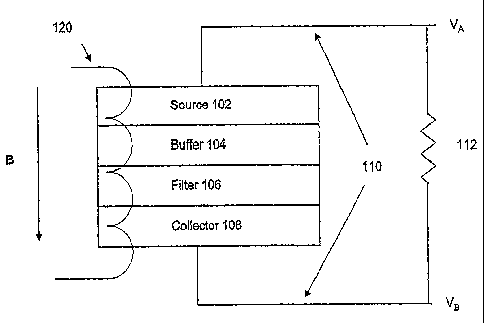
100081 Figure 1 illustrates one embodiment of a current source.
[00091 Figures 2a, 2b, 2c show a band diagram illustrating electron
transitions
in an embodiment of the source in Fig. 1.
[00101 Figures 3a, 3b are graphs of the rate of excitations vs. temperature
and
the minimum detection temperature vs. Ni composition, respectively, in the
embodiment of the source in Fig. 1.
2
CA 02633028 2008-06-11
WO 2007/070524 PCT/US2006/047403
[00111 Figures 4a, 4b, and 4c are graphs of L for W, Pd, and Ni vs.
temperature, respectively, in the embodiment of the source in Fig. 1.
[00121 Figures 5a and 5b illustrate band diagrams of a source and different
buffers in the embodiment of Fig. 1.
[00131 Figures 6a, 6b, 6c show band diagrams of embodiments of different
current sources.
[00141 Figures 7a, 7b, 7c show band diagrams and associated equivalent
circuits and current-voltage graphs of embodiments of different current
sources.
[00151 Figure 8 shows a band diagram of the filter-collector region of an
embodiment of a current source.
[0016] Figure 9 shows a band diagram of the source-buffer-filter region of an
embodiment of a current source.
[0017] Skilled artisans appreciate that elements in the figures are
illustrated
for simplicity and clarity and.have not necessarily been drawn to scale.
DETAILED DESCRIPTION
[00181 A current source and method of producing the current source is
provided. The current source includes at least a metal layer and a
semiconductor
layer. An electrical connection is provided to the metal layer and
semiconductor
layer and a magnetic field applier may be provided. The interaction of the
layers
produces a spontaneous current. The movement of charge across the current
source produces a voltage, which rises until a balancing reverse current
appears.
If a load is connected to the current source, current flows through the load
and
power is dissipated. The energy for this comes from the thermal energy in the
current source, and the device gets cooler.
[0019] Referring to Fig. 1, in one embodiment, the current source 100
includes four layers 102, 104, 106, and 108. The four layers include a source
102, a buffer 104, a filter 106, and a collector 108. Each of the four layers
contacts at least one other layer; i.e. the source 102 contacts the buffer
104, the
buffer 104 contacts the filter 106, and the filter contacts the collector 108.
Leads
110 from which current may be extracted are electrically connected to the
source
102 and the collector 108. A magnetic field B may be applied in a direction
3
CA 02633028 2008-06-11
WO 2007/070524 PCT/US2006/047403
substantially perpendicular to the layers 102, 104, 106, 108 via a magnetic
source
120, such as a coil.
[0020] Although the layers 102, 104, 106, and 108 are shown as single layers,
one or more of these layers 102, 104, 106, and 108 may be multiple layers. The
interaction of the source 102, buffer 104, filter 106, and collector 108
produces a
spontaneous current. The movement of charge across the current source 100
produces a voltage, which rises until a balancing reverse current appears. If
a
load 112 is connected to the current source 100 through leads 110, current
flows
through the load 112 and power is dissipated. The energy for this comes from
the
thermal energy in the current source 100, and the current source 100 gets
cooler.
[0021] The source 102 is a metal or mixture of metals which has localized
states at the bottom of the conduction band. The localized states 204 at the
bottom of the conduction band 202 are shown schematically in Fig. 2a.
Interactions between electrons near the Fermi surface and the localized
electrons
trapped on the localized states 202 occasionally elevate the localized
electrons to
the Fermi surface as shown in Fig. 2b as transition 1. The energy for this
transition is between about I and 6 eV and comes from the energy of collisions
of
the localized electron with multiple free electrons. Normal collisions return
an
electron to the localized state and produce excess electrons above the Fermi
surface and excess holes below, as shown in Fig. 2b as transition 2 and in
Fig. 2c.
These energetic electrons and holes may be the source of the cu rent:
Interactions
between localized electrons and phonons can also elevate the localized
electrons
to the Fermi surface. In this case the energy for the transition comes from
'multiple phonons.
[0022] A suitable source metal has at least two properties. First, the source
has localized states at the bottom of its conduction band. These states should
have an energy E, about 0.01 eV < E < about 0.05 eV below the bottom of the
conduction band. The number of these states should be low enough so that their
overlap is small. This is to say that the number of states should be small
enough
so that the levels are not degenerate (i.e. they do not spread into an
impurity band
that merges with the conduction band). In one embodiment, the concentrations
are less than about 1000 ppm (part per million). Second, the probability of
4
CA 02633028 2009-07-20
transition 1 shown in Fig. 2b occurring in the source should be large enough
to produce
enough energetic electrons. Localized states in the metal can be produced in
three ways:
disorder in the metal, small amounts of impurities, or an applied magnetic
field (shown in
Fig. 1).
[0023] A disordered metal, or a metal with some degree of disorder, can be
defined
as a metal whose potential for conduction electrons is non-periodic. For a
small amount of
disorder, it may be possible to divide the potential into two parts, Vp (which
has the
periodicity of the lattice) and Vnp (which is non-periodic). The relative size
of Vnp and Vp
can be taken as a measure of the degree of disorder. There are a number of
ways for a metal
to have disorder. It may be an alloy of two or more metals whose atoms are
randomly
distributed throughout the lattice. It may have a number of impurities whose
size is
significantly different from the size of the host metal atoms. The impurity
atoms push their
nearest neighbors to slightly different positions, those atoms push their
nearest neighbors,
and so on. A pure metal may consist of more than one stable isotope. The
different isotopes
will be randomly distributed throughout the lattice, producing a slightly
disordered potential.
The metal may be in a metastable mixture of two different crystal forms, in a
structure called
random stacking. Or the metal may be a transition metal with localized
magnetic moments
pointing in random directions. The non-periodic potential will produce
localized states at
the bottom of the conduction band through the process of Anderson
localization. Disordered
metals can be divided into two classes, pure metals and mixtures. Atoms of
transition metals
and rare earth metals have partially filled d-shells. Transition metals are
elements that are
characterized by the filling of an inner d electron orbital (or shell) as
atomic number
increases. Transition metals include the elements with atomic numbers 21 to
30, 39 to 48, 58
to 80, and 89 to 112, and in particular, from titanium to copper and those
elements lying in
the columns therebelow in the International Union of Pure and Applied
Chemistry (IUPAC)
periodic table.
[0024] The transition metals have randomly oriented magnetic moments due to
the
incomplete filling of the d shell. The random orientation of the magnetic
moments of these
shells may produce a disordered potential for the conduction electrons in
these metals. In
particular, the potential that a conduction electron experiences while on an
atom may depend
on the relative orientations of the magnetic moments of the atom and its
nearest neighbors.
Most of the transition metals have crystal structures in which every atom has
12 nearest
neighbors. Most of the remaining transition metals have structures with 8
nearest neighbors.
It may be that, for an atom to have a low enough potential to produce a
localized state with E
> about 0.01 eV below the bottom of the conduction band, 9 of its nearest
neighbors have
magnetic moments aligned with its magnetic moment, and 3 are anti-aligned with
its
CA 02633028 2009-07-20
magnetic moment. With randomly aligned moments, the fraction of atoms with
localized
states may be low enough to satisfy the conditions listed above.
[0025] The normal situation is more complicated, because most d shells have
more
than two possible orientations, (j>1/2, where j is the angular momentum
quantum number),
but the same principle may apply. In the ferromagnetic metals Fe, Co, and Ni,
the relative
orientations of neighboring magnetic moments is not random for T<TC ( the
Curie
temperature). At T=O, all the magnetic moments are aligned and there is no
possibility of an
atom having a lower potential than the
5A
CA 02633028 2008-06-11
WO 2007/070524 PCT/US2006/047403
average- As temperature is increased, disorder increases. At some temperature
To it becomes possible for some atoms to have localized states. As the
temperature is further increased, the number of localized states increases.
[0026] In mixtures of two or more metals, the random positions of the
different atoms may produce a disordered potential. Mixtures can be comprised
of metals that normally dissolve in each other, such as Ni-Cu, Pd-Ag, Pt Au,
or of
metals that do not normally mix but can be deposited in a mixed state.
Examples
of metals that do not normally mix include Fe-Co and Ti-V.
[0027] Turning away from disordered metals to metals containing impurities,
some impurities in certain metals may produce localized states. For non-
transition metals (such as those in col. 2 and 13-17 in the new IUPAC
notation),
the impurity metal should be of the same column of the periodic table as the
parent metal, and usually lower in the column. For instance; Ga or In may be
used as impurities in Al or K or Rb may be used as impurities in Na. However,
there are also exceptions to these rules; for instance, Bi impurities in Pb
produce
localized states. For transition metals, the impurity metal can be of the same
column as. the parent metal. or of a column to the right of the column of the
parent
metal. Cu in Ni is one such example.
[0028] The concentration of the impurity atoms can range from less than 1
part per million up to an upper limit in which the isolated localized states
overlap
and merge to become the disordered localized states. For low concentrations
(<1000 ppm - part per million),.the number of energetic electrons produced is
proportional to the concentration of impurities.
[00291 Rather than provide impurities, an external magnetic field can be
applied to produce the current source. If a magnetic field is applied to a
metal,
states that are localized in two dimensions, called Landau states, are
produced at
the bottom of the conduction band. To produce the Landau states, the metal is
substantially free of disorder. For example, the purity of a non-transition
metal
should be greater than about 99.9%. (e.g.. less than 10 ppm). As shown in Fig.
1,
the magnetic field B is applied substantially perpendicular to the surface of
the
source 102.
6
CA 02633028 2008-06-11
WO 2007/070524 PCT/US2006/047403
[00301 Ordinarily, the excitation of an electron from a localized state at the
bottom of the conduction band to the Fermi surface happens extremely rarely.
It
is possible to increase the frequency of this event through a process which
will
subsequently be referred to as probability amplification. Probability
amplification can occur in transition metals as a result of the interaction of
the
incomplete d-shells of neighboring atoms and thermal vibrations (phonons) of
the
atomic lattice. In non-transition metals, probability amplification can be
produced close to the physical surface of the metal (e.g. within about 100A)
by
the application of an alternating electric field and a non-parallel magnetic
field B.
100311 In a given metal, a probability amplification value can be assigned for
electrons in each band and for phonons. For instance, a transition metal with
an S
band and a D band has probability amplification values PAS (S-band), PAD (D-
band), and PAL (phonon).in.many. metals, the intrinsic probability
amplification
of electrons is large compared to externally produced probability
amplification,
making the probability amplification essentially independent of external
factors
such as applied magnetic field, applied electric field, temperature, and
pressure.
For metals with one conduction band, the value of probability amplification
for
electrons varies inversely with the ease with which the electrons move from
atom
to atom. S-electrons move most easily, so PAS is relatively small. P-electrons
move less easily, so PAP (probability amplification in the P-band) is larger.
D-
electrons move much less easily, so PAD is much larger. F-electrons in rare-
earth metals move with so much difficulty that they do not form a band at all,
so
these rules do not apply to them.
[00321 The same trend applies from metal to metal. In the Cr, Mo, W group,
d-electrons move easily, so PAD is relatively small. As one moves to the right
in
the periodic table, d-electrons become less mobile and PAD increases, until
the
Ni, Pd, Pt group, where PAD is greatest. There is the same variation within
columns. The d-shell in row 5 atoms tends to be deeper than in row 4 or 6
atoms.
So for instance, PAD in Pd is larger than PAD in Ni or Pt. For metals with
more
than one conduction band, interactions between electrons in different shells
in an
atom can influence the probability amplification of a band. In transition
metals,
PAS is larger (but still much smaller than PAD) than PAS in non-transition
7
CA 02633028 2008-06-11
WO 2007/070524 PCT/US2006/047403
metals because of the interaction between the s and d shells. PAS will be
largest
in those transition metals with the largest PAD.
[00331 The probability amplification of phonons PAL and electrons can be
influenced by external factors. One way PAL can be- achieved close to the
physical surface (e.g. within about 100 A) is, as indicated above, by the
application of an alternating E-field and a B-field. The electric and magnetic
fields are not parallel to each other.
[0034] One way to apply the electric field is to have the neighboring layer or
layers (i.e. the buffer layer 104 or-the f lter layer 106) be a material which
has a
high density of optically active localized phonon-modes. The material thus has
a
large number of charged atoms that are vibrating, producing an alternating
electric field. This alternating electric field is able to penetrate a short
distance
into- the source 102. Typical frequencies of vibration of the charged atoms
extend
between about 1012 to 1013 Hz. For a vibration frequency of about 1013 Hz, for
"
example, -Cu has a skin depth of 200A. For other metals, the depth may be
different.
[00351 The magnetic field can be applied externally. In different
embodiments, the magnetic field can be applied by placing the current source
100
in a solenoid 120 (as shown in Fig. 1) or by placing permanent magnets nearby.
The output of the source 102 can then be controlled by changing the strength
of
the applied magnetic field.
[00361 In addition, the probability amplification increases with temperature.
At low temperatures, the number of excitations per unit time and unit volume,
dn/dt, is below the detectable limit, as shown in Fig. 3a. At a finite turn on
temperature, T0, dn/dt becomes detectable and rises rapidly with temperature.
The value of T,, for a given metal is determined by the nature of the
localized
states and the effectiveness of probability amplification. The value of To for
mixtures can be varied continuously over a predetermined range by varying the
composition of the particular mixture. In Cu-Ni alloys, for instance, disorder
is
greatest close to 50% Cu-50% Ni. Only the Ni atoms have incomplete d-shells so
the probability amplification increases with increasing Ni content. A graph of
Ta
8
CA 02633028 2009-07-20
versus composition for this series of alloys is predicted to have the form
shown in Fig. 3b.
[0037] The thickness of the source 102 can vary from few atomic thicknesses
(about
IOA) to a maximum thickness desired for the overall current source 100. For
thicknesses
below about 100A, a buffer may be used on one or both sides of the source 102.
[0038] Since transition metals have disorder and probability amplification,
they can
all be considered candidates to be source metals. Many of the transition
metals have turn on
temperatures To that are too high to be practical. An upper bound for the turn
on temperature
may be estimated for some metals using thermal conductivity, electrical
resistivity, and
thermopower data at a series of temperatures. The Lorenz number L is defined
by equation
(1):
(1) L=(k*r)/T+S2
[0039] In equation (1), k is the thermal conductivity, r is electrical
resistivity, and S
is thermopower of the metal. L should approach a magnitude of 2.443 x 10' watt-
ohm /
( C)2 at high temperatures. Seven metals which have significant deviations
from this are Mo,'
W, Ni, Pd, Pt, Fe and Co. Data for Pd, W, and Ni are shown in Tables 1, 2a and
2b, and 3
and illustrated in Figs. 4a, 4b, and 4c. AK in the tables is the amount of
thermal conductivity
in addition to that due to the conduction electrons that must exist in the
metal to achieve the
measured L. AK can be calculated from eq.(1) using measured k, r, and S. If
this additional
thermal conductivity comes from lattice thermal conductivity (the only
conventional
possibility), its value should be proportional to l/T, for temperatures
greater than the Debye
temperature of the metal. Any part of AK not attributable to lattice thermal
conductivity,
especially a AK increasing with temperature may be an indication of thermal
conductivity
from excitation of electrons from localized states- meaning both localized
states and
probability amplification are present in the metal. However, while these seven
metals may
make good source metals, use of L vs. T data alone may not rule out metals to
use.
Excitation of localized states does not always affect thermal and electrical
conductivity.
Mixtures of metals can be investigated in the same way. Cu-Ni, Ag-Pd, and Au-
Pt alloys
may be good source metals. The rate of excitation of localized states in a
metal can be
increased by increasing the amount of disorder, or by increasing the
probability
amplification. to have a measurable effect on thermal conductivity, and thus
on L, the
localized states should be large (-l 000A or more) with a high rate of
excitation. Spread out
localized states imply low disorder, so to achieve a high rate of excitation a
relatively large
probability amplification is needed. So the deviations in L seen for the seven
metals
indicates they have a high degree of probability amplification. Nearest
neighbors on the
periodic table to these seven could be expected to have higher than average
probability
amplification values. For mixtures of metals, the amount of disorder can be
greatly
9
CA 02633028 2009-07-20
increased, so the level of probability amplification does not need to be as
large. Therefore all
transition metals are good candidates for source metals in alloys.
Table 1 Palladium (Pd)
T(K) Thermal Electrical Thermopower L+S2 AK
conductivity resistivity (microvolts/deg) (x108) (watts/cm*deg C)
(watts/cm*deg) (ohm-cm)*106
100 .737 2.595 2.0 1.91 0.066
200 .707 6.858 -4.85 2.43 0.081
300 .721 10.765 -10.69 2.60 0.090
400 .741 14.422 -13.6 2.69 0.098
600 .797 21.056 -19.3 2.83 0.105
800 .870 26.856 -25.71 2.99 0.142
1000 .949 31.878 -32.26 3.13 0.183
1200 1.02 36.168 -38.46 3.22 0.209
Table 2a Tungsten (W)
T(K) Thermal Electrical L(x108) AK
conductivity resistivity (watts/cm*deg C)
(watts/cm* deg) (ohm cm)* 106
300 1.76 5.48 3.21 0.576
400 1.59 7.91 3.14 0.452
600 1.37 13.14 3.00 0.308
800 1.26 18.78 2.96 0.238
1000 1.19 24.72 2.94 0.211
1200 1.14 30.9 2.94 0.191
1600 1.06 44.03 2.92 0.186
2000 1.01 57.62 2.91 0.162
2400 .97 72.04 2.91 0.156
Table 2b Tungsten
Tl T2 nK(T1)/zK(T2) LK(T1)/AK(T2)
theoretical
400 600 1.47 1.50
600 800 1.29 1.33
800 1000 1.13 1.25
1000 1200 1.10 1.20
1200 1400 1.02 1.17
Table 3 Nickel (Ni)
T(K) Thermal Electrical Thermopower L+S2 AK
conductivity resistivity (microvolts/deg) (x108) (watts/cm*deg C)
(watts/cm*deg) (ohm-cm)*106
100 1.64 .986 -8.50 1.62 0.21
150 1.22 2.237 -10.98 1.83 0.11
CA 02633028 2009-07-20
200 1.07 3.703 -13.45 2.00 0.07
250 .975 5.384 -16.35 2.13 0.06
300 .907 7.237 -19.52 2.23 0.05
400 .802 11.814 -23.99 2.43 0.07
500 .722 17.704 -25.75 2.62 0.10
600 .656 25.554 -22.16 2.84 0.13
1000 .718 41.496 -29.85 3.07 0.15
1200 .762 46.728 -35.42 3.09 0.167
[0040] The tables illustrate three cases. AK for Pd increases with T
monotonically
from 100K to 1200K. It is hard to estimate a To but 200K is a reliable upper
bound. AK
decreases with T at low temperatures for Ni, reaches a minimum at 300K, and
increases with
T for T>300K. An upper bound of 300K is a safe upper bound. This is consistent
with our
understanding of disorder in Ni. Nickel is ferromagnetic below 620K. At OK all
the
localized magnetic moments are aligned and there is no disorder due to them.
As the
temperature is increased, more and more magnetic moments become misaligned
until they
are all pointing in random directions at 620K. At a temperature between OK and
620K, there
will be the right amount of disorder, large enough to have excitations and
small enough to
have large localized states. Fe and Co show the same behavior, with T0(Fe)
about 370K and
T0(Co) about 500K. Small amounts of impurities in these three ferromagnetic
metals can
reduce their Curie temperatures, which would also reduce To. AK for W never
increases
with temperature but the ratios of AK for two different temperatures (as shown
in Table 2b)
differ from what would be expected for pure lattice conductivity and are
consistent with an
additional contribution to thermal conductivity from excitation of localized
states that is
constant with temperature. It is difficult to estimate a To, but excitations
appear to be present
at T=800K. Note that these estimates of To are for the interiors of the metals
and values of To
near the surface may be different because of different levels of probability
amplification near
the surface.
[0041] The seven metals which may be the best candidates for source metals
among
the transition metals are Mo, W, Ni, Pd, Pt, Fe, and Co. Each of the L vs. T
data for these
metals indicates the presence of excitations. The transition metals that are
in the same
column as one of these metals, but whose L vs. T data show no evidence of
excitations, may
also be promising. These metals include Cr, Ru, Rh, Os, and Ir. The rest of
the transition
metals may be poorer candidates than the metals already mentioned.
[0042] Source metals with isolated impurity atoms have already been discussed.
If
the host metal is a transition metal, probability amplification can be
intrinsic to the metal. If
the host metal is a non-transition metal without impurities generating
disorder, probability
amplification may be provided from outside the metal. If the localized states
are produced by
11
CA 02633028 2009-07-20
a magnetic field, the metal is essentially free of disorder without the
application of the
magnetic field. In this case, any pure non-transition metal may be used, for
example Al or
Sn. The magnetic field producing the Landau states can be used in probability
amplification.
11A
CA 02633028 2008-06-11
WO 2007/070524 PCT/US2006/047403
[0043] Turning to the buffer 104, the buffer 104 permits the excitation
processes in the source 102 to occur close enough to the surface of the source
102
so that an appreciable fraction of the excess electrons and excess holes far
from
the Fermi energy reach the surface of the source 102. For this to happen, the
bottom of the conduction band in the source 102, where the localized states
are
disposed, lines up with a forbidden band of the buffer 104. A suitable buffer
104
may be a metal, insulator or semiconductor. The buffer 104 should be thin
enough (about 10-50A) so that a -substantial fraction of the energetic charges
(electrons or holes) pass through to the filter 106. For example, if the
buffer 104
is an insulator, the charges from the source 102 may tunnel through the buffer
104 to the filter 106.
[00441 Two cases are illustrated in Figs. 5a and 5b. Figure 5a illustrates the
band diagram of a material that is not suitable as a buffer for a particular
source.
As shown in Fig. 5a, the localized states and bottom of the conduction band in
the
source 102 are aligned with the conduction band of the buffer 104, and the
tops of
the conduction band of the source 102 and buffer 104 are offset by energy zEi.
The presence of the material forming the buffer 104 destroys the conditions in
the
source 102 in which excitations occur close to the interface. In this case,
the
number of energetic electrons increases with the distance from the interface
as
shown in the accompanying graph. As shown in Fig. 5b, the localized states and
bottom of the conduction band in the source 102 are offset by energy AE2, and
the
tops of the conduction band of the source 102 and buffer 104 are aligned. If
the
bands of the filter 106 line up correctly with the source 102, the buffer 104
can be
eliminated and the filter 106 may then serve as the- buffer. In this case, the
number of energetic electrons is constant with the distance from the interface
as
shown.
[0045] Turning. to the filter 106, the filter 106 functions to conduct the
high
energy charges originating from the source 102 and to block the flow of
electrons
.close to the Fermi surface. In one embodiment, the filter 106 comprises a
semiconductor, e.g. an elemental semiconductor such as Si or Ge or a compound
semiconductor such as a III-V semiconductor. Alternatively, the filter 106 may
comprise an insulator such as SiO2, CaO, or AIM. In various embodiments, the
12
CA 02633028 2008-06-11
WO 2007/070524 PCT/US2006/047403
filter 1.06 may conduct high energy electrons and/or holes while blocking
other
charge carriers. For example, in one embodiment, the filter 106 conducts the
high energy electrons and blocks all other charges. In another embodiment, the
filter 106 conducts high energy holes and blocks all other charges. In another
embodiment, both high energy electrons and high energy holes are transported
through the filter 106. In this last case, the polarity of the output current
of the
current source 100 is determined by which charge carrier dominates. These
embodiments are described below with regard to Fig. 6 in more detail.
[00461* The collector 108 may be a metal or a heavily doped semiconductor
(e.g. about 1017 cm 3 or more dopants) and can be any thickness above about 1
OA.
If outside electrical connection is made to the collector 108, it should be at
least
about 1 micron thick. The collector 108 may chosen to make an ohmic contact
with the semiconductor filter 106 in some cases, and in other cases to make a
rectifying contact. As shown in Fig. 8, surface state pinning of the Fermi
level
largely determines the size of the barrier between metal and semiconductor. An
ohmic contact between the filter 106 and collector 108 can be made in that
case
by heavily doping the collector side of the filter 106. A rectifying contact
can be
made at the buffer-filter interface by lightly doping the semiconductor on the
buffer layer side as shown in Fig. 9. The choice of collector metal in this
case
can be based on compatibility with neighboring layers. Sn, for example, may be
a good choice.
[00471 If the filter 106 is a 11-VI semiconductor or other semiconductor that
does not have surface state pinning, the nature of the contact between the
semiconductor and metal may be determined by the relative positions of the
Fermi level of the metal and the conduction and valence band edges of the
semiconductor. For instance, Pd and Pt form a rectifying contact with ZnO. Sn
and Al form an ohmic contact with'ZnO.
[00481 Excitation processes in the source metal cause there to be more
electrons and holes far from the Fermi energy than what is predicted by .
equilibrium statistical mechanics. The buffer 104 allows those energetic
charges
to reach the surface of the source 102 and to pass into and through the buffer
104,
into the filter 106. The filter 106 allows some of the high energy charges to
pass
13
CA 02633028 2008-06-11
WO 2007/070524 PCT/US2006/047403
through into the collector 108. Because the collector 108 is an ordinary
metal, it
does not have a surplus of high energy charges that are able to pass through
the
filter 106. Consequently, charge builds up in the collector 108 and an
electric
field develops in the filter 106. The field grows until a balancing current
flowing
in the opposite direction develops. If the field grows too large, breakdown
will
occur in the semiconductor, destroying its ability to filter.
[0049] In addition, the filter 106 and collector 108 permit sufficient reverse
current to flow so that breakdown does not occur. This can be done in a number
of ways. If the semiconductor is thin enough (about 50A), tunneling can occur
from the collector 108 to the buffer 104 or source 102. If the semiconductor
has
enough defects, such as amorphous silicon or germanium, conduction through
defect states in the middle of the forbidden band can occur. If the collector
metal
forms an ohmic contact with the filter layer semiconductor, a Schottky diode
is
formed. As charge builds up in the collector, the Schottky diode becomes
forward biased in the collector-source direction and a balancing reverse
current
can develop.
[0050] If the semiconductor in the filter 106 is undoped, thus having an
intrinsically high resistance, the thickness of the filter 106 is limited to
about 100
to 200A to prevent space-charge effects, which will produce instabilities in
output
current. If the semiconductor is doped or low resistance, the thickness can be
above about 100A.
[0051] Possible semiconductors include Si, Ge, GaAs, AlAs, AISb, SnO2,
among many others. Insulators that can be used include MgO and CaO. If the
semiconductor also provides probability amplification as previously discussed,
it
has a large number of localized phonon modes. Mixture semiconductors include,
.such as AIGai_XAs or AIAs,,Sbl.,r or-ZnOXS1,, where x can vary from about
0.25
to 0.75. These mixtures are good semiconductors but have a disordered phonon
spectrum with many localized modes. Those modes provide an alternating
electric.field, which when combined with an externally applied magnetic field
provides probability amplification in the source. More complicated
= semiconductors such as organic semiconductors also can be used.
14
CA 02633028 2008-06-11
WO 2007/070524 PCT/US2006/047403
[00521 As described, the current source 100 includes a series of thin layers
102, 104, 106, and 108 of metals and semiconductors and/or insulators. The
layers 102, 104, 106, and 108 maybe fabricated by vacuum deposition such that
they contact each other. Different vacuum deposition technologies may be
suitable for fabrication of the current source 100. These vacuum deposition
technologies include sputtering, chemical vapor deposition, and electron beam
.
evaporation.
[00531 Deposition takes place in a vacuum chamber. The chamber includes a
vessel capable of maintaining a vacuum. The chamber also has electrical
feedthroughs that allow current to be fed to wires inside the chamber and a
motion feedtbrough, which allows a target inside the vessel to be moved,
connected via vacuum tubing and valves to vacuum pumps. The vacuum
chamber maintains a vacuum of less than about 10-6 torr during deposition.
Material to be evaporated is placed in conical baskets made of tungsten
filament,
for example. If the material to be evaporated is in the form of wire or foil,
it can
simply be wrapped around a tungsten filament. One end of the tungsten filament
is connected to an electrical feedthrough, while the other end of the tungsten
filament is connected to a wall of the vessel, which serves as electrical
ground. If
voltage is applied to the electrical feedthrough from the outside, current
flows
through the filament, heating it and the material in contact-with it. With
enough
current, the material gets hot enough to evaporate. Since it is in a vacuum,
the
atoms are emitted substantially uniformly in all directions. The target is
placed
on a carrier connected to the motion feedthrough so that it can be moved into
optimal position to receive the evaporated material. Since the material, to a
good
approximation, is emitted substantially uniformly in all directions, the
amount
that hits the target, and thus the thickness of the. layer, can be calculated
from
simple geometry and knowledge of the amount of material in the basket and the
distance from the basket to the target. When the deposition of one layer is
completed, the target is moved to a new position, current is run through
another
basket holding material for the next layer and the process is repeated. In
this
way, layers fabricated without a large amount of impurities occurring at the
interface. Care is taken in the selection of material for adjoining layers as
the
CA 02633028 2008-06-11
WO 2007/070524 PCT/US2006/047403
deposited material may not uniformly coat the target but instead form islands
on
the top of the target, especially for exceedingly thin layers.
[00541 An example device contains a steel substrate on which a sequence of
layers is formed. These layers may include 1000A of Sn, 100A of Ge, 30A of Pb,
and 1000A. of Pd. The 30A layer of Pb forms the buffer. The sequence can be
repeated as many times as desired: After the desired number of repetitions of
this
sequence a final layer of 1 micron of Sn is deposited. If vacuum is broken to
reload material, it may be done after the Pd deposition. This will introduce a
thin
layer (of about 20A) of PdO between the Pd .and the next Sri layer. The i OOOA
layer of Sri forms the collector layer, the Ge forms the filter, the 30A layer
of Pb
forms the buffer, and the Pd forms the source.
[00551 The steel substrate may be a conventional steel washer having a
diameter of about 1 cm. The steel substrate is cleaned, rinsed with distilled
water,
and dried using nitrogen gas, for example. The steel substrate may also be
buffed
to shine with a reasonable brightness using a soft cotton cloth. A single
layer,
such as Sn, may be deposited. If this layer is capable of being removed by an
adhesive, such as a piece of Scotch tape, the substrate is cleaned again.
[00561 After a suitable cleaning, the disk is placed on carrier and deposition
material is placed in baskets or on wires. To deposit the above layers, Sri is
placed in a basket, Ge in a basket, Pb in a basket, and Pd wires wrapped
around a
tungsten filament. The system is evacuated and continuously pumped until a
vacuum of 10-6 torr is achieved. This takes about 2 hours in one example of a
vacuum system,
[00571 When the above vacuum is achieved, deposition may begin. First,
1000A of Sri is deposited, then 100A of Ge is deposited, followed by 30A of
Pb.
The Ge at this stage is .in an amorphous form. The substrate is heated to 400K
for
30 minutes to change the amorphous Ge to a polycrystalline Ge layer. After
forming the polycrystalline Ge layer, 1000A of Pd is deposited in which the Pd
is
doped with Ag. To repeat this sequence, the chamber is opened up and reloaded
with Sn, Ge,.Pb, and Pd. The chamber is evacuated and.the sequence is
repeated.
To finish, a 1 micron layer of Sn is deposited. Metal conductors are then
attached
16
CA 02633028 2008-06-11
WO 2007/070524 PCT/US2006/047403
to the top and bottom of the disk with conductive epoxy or soldered to make
electrical connections.
[00581 Figures 6a, 6b, 6c show band diagrams of embodiments of different
current sources. In each of these embodiments, the top of the conduction band
in
the source 102 is aligned with the top of the conduction band of the collector
108.
In the embodiment shown in Fig. 6a, electrons that have been excited in the
source 102 tunnel through the buffer 104 and transit across the filter 106
into the
empty part of the conduction band of the collector 108. As shown, the top of
the
valence band of the filter 106 is below (i.e. has a lower energy than) the
bottom
of the conduction band of the source 102. In other words, the bottom of the
bandgap of the filter 106, which is either a semiconductor or insulator, is
below
the bottom of the conduction band of the source 102. Thus, as there are no
states
in the bandgap of the filter 106, holes generated in the source 102 by the
excitation of the electrons remain in the source 102.
[00591 In the embodiment shown in Fig. 6b, however, the valence band of the
filter 106 extends to above the bottom of the conduction band of the source
102
while the bottom of the conduction band is at a higher energy than that of the
excited electrons. Thus, holes in the source 102 tunnel through the buffer 104
and transit across the filter 106 into the occupied part of the conduction
band of
the collector 108 while the excited electrons generated in the source 102
remain
in the source 102 as there are no states in the bandgap of the filter 106.
[00601 * In the embodiment shown in Fig. 6c, both electrons, that have been
excited in the source 102 and the holes left in the localized states, tunnel
through
the buffer 104 and transit across the filter 106. The electrons transit into
the
empty part of the conduction band of the collector 108 and the holes transit
into
the occupied part of the conduction band of the collector 108. As can be seen,
the
bandgap of the filter 106 is small enough such that the top of the valence
band of
the filter 106 is above the bottom of the conduction band of the source 102
and
the bottom of the conduction band of the filter 106 is below the energy level
of
the excited electrons in the source 102.
[00611 Figures 7a, 7b, and 7c show band diagrams and associated equivalent'
circuits and current-voltage graphs of different current sources. As shown in
Fig.
17
CA 02633028 2008-06-11
WO 2007/070524 PCT/US2006/047403
7a, the electrons transit from the source 102 to the empty portion of the
conduction band of the collector 108, forming the forward current I0. In
addition,
electrons in the occupied portion of the conduction band of the collector 108
tunnel from the collector 108 to the collector of the source 102 through the
bandgap of the filter 106, thereby forming the reverse current IT. The
magnitude
of the reverse current IT is proportional to the voltage across the current
source
100, the difference between the energy at the top of the occupied part of the
conduction band in the collector 108 and the bottom of the conduction band in
the
filter 106, and exponentially decreases with increasing thickness of the
filter 106.
As the equivalent circuit diagram of the current source 100 looks like an
ideal
current source with a resistor R in parallel (the resistance of the current
source
100), as shown, the voltage across the current source 100 is linear with the
resistance R. Thus, while the forward current IQ is constant, the reverse
current IT
increases linearly with the voltage V0 across the current source 100.
[00621 As shown in Fig. 7b, another mechanism that can give rise to a reverse
current is a current generated by defect hopping in the bandgap of the filter
106.
This is to say that, if defects exist in the filter 106 due to imperfections
in the
lattice of the filter 106, for example, and these defects create defect states
in the
bandgap, a defect current, ID may be generated. Similar to Fig. .7a, the
equivalent
circuit diagram of the current source 100 in Fig. 7b looks like an ideal
current
source with a resistor R in parallel (the resistance of the current source
100).
Thus, while the forward current Io is constant, the reverse current ID
increases
linearly with the voltage VO across the current source 100.
[00631 As shown in Fig. 7c, another mechanism.that can give rise to. a reverse
current is a current generated by an internal electric field established in
the filter
106 by the presence of the source 102 and the collector 108. This is to say
that,
when the current source 100 is fabricated, the conduction and valence band
edges
of the filter 106 may be pinned at the interfaces between the collector 108
and the
buffer 108 (if present). This, in turn, can cause the conduction and valence
band
in the filter 106 to bend when the conduction bands of the source 102 and the
collector 108 align and thus establish an internal electric field. In this
case, the
equivalent circuit diagram of the current source 100 in Fig. 7c looks like an
ideal
18
CA 02633028 2012-01-12
WO 2007/070524 PCT/US2006/047403
current source with a diode D in parallel (the resistance of the current
source
100). As the current in a diode increases exponentially with voltage, again
while
the forward current L is constant, the reverse current IDTODE increases
linearly
with the voltage Va across the current source 100. .
[0064] Note that the specification and figures are to be regarded in an
illustrative
rather than a restrictive sense, and all such modifications are intended to be
included
within the scope of present invention. As used herein, the terms "comprises,"
"comprising," or any other variation thereof, are intended to cover anon-
exclusive
inclusion, such that a process, method, article, or apparatus that comprises a
list of
elements does not include only those elements but may include other elements
not
expressly listed or inherent to such process, method, article, or apparatus.
[0065] It is therefore intended that the foregoing detailed description be
regarded as illustrative rather than limiting, and that it be understood that
it is the
following claims, including all equivalents, that are intended to define the
scope of this invention. Nor is anything in the foregoing description intended
to disavow scope of the invention as claimed or any equivalents thereof.
19