Note : Les descriptions sont présentées dans la langue officielle dans laquelle elles ont été soumises.
CA 02633437 2008-06-04
Attorney Docket No. H28277
PATENT
Indicia Reading Terminal Processing Plurality of Frames of Image Data
Responsively
to Trigger Signal Activation
Cross Reference to Related Applications
[0001] This application claims priority under 35 U.S.C. 119(e) to Provisional
Patent
Application No. 60/933,022, entitled "Indicia Reading Terminal Processing
Plurality of
Frames of Image Data Responsively To Trigger Signal Activation" filed June 4,
2007. This
application is also related to U. S. Patent Application (Not Yet Assigned)
(Attorney Docket
No. H28366) entitled "Indicia Reading Terminal Having Multiple Setting Imaging
Lens"
filed concurrently herewith. Each of the above applications is incorporated
herein by
reference in its entirety.
Field Of The Invention
[0002] The invention relates to data collection registers in general, and
specifically, to an
indicia reading terminal.
Background Of The Invention
[0003] Indicia reading terminals for reading decodable indicia are available
in multiple
varieties. For example, minimally featured indicia reading terminals devoid of
a keyboard
and display are common in point of sale applications. Indicia reading
terminals devoid of a
keyboard and display are available in the recognizable gun style form factor
having a handle
and trigger button that can be actuated by an index finger. Keyboard and
display equipped
indicia reading terminals are also presently available. Indicia reading
terminals having
keyboards and displays are also available. Keyboards and display equipped
indicia reading
terminals are commonly used in shipping and warehouse applications, and are
available in
form factors incorporating a display and keyboard. In a keyboard and display
equipped
indicia reading terminal, a trigger button for actuating the output of decoded
messages is
typically provided in such locations as to enable actuation by a thumb of an
operator. Indicia
reading terminals in a form devoid of a keyboard and display or in a keyboard
and display
equipped form are commonly used in a variety of data collection applications
including point
of sale applications, shipping applications, warehousing applications,
security check point
applications, and patient care applications. Some indicia reading terminals
are adapted to
read bar code symbols including one or more of one dimensional bar codes
stacked 1D bar
1
CA 02633437 2008-06-04
Attorney Docket No. H28277
PATENT
codes and two dimensional bar codes. Other indicia reading terminals are
adapted to read
OCR characters while still other indicia reading terminals are equipped to
read both bar code
symbols and OCR characters. Indicia reading terminals commonly include
prepackaged
single image sensor imaging modules. An example of a prepackaged single image
sensor
imaging module is the 5X00 Engine Series imaging module available from Hand
Held
Products, Inc. of Skaneateles Falls, New York. Such imaging modules commonly
carry
illumination (e.g., light source) and imaging components. In the 5X00 Engine
Series imaging
module, commands to establish the imaging parameter settings (e.g., gain,
exposure) are
transmitted from a motherboard disposed image capture and processing circuit
to an imaging
module disposed image sensor integrated circuit over a two wire interface bus
wherein the
two wire interface bus includes a pair of contacts of the imaging module. In
the 5X00
imaging module, commands for switching between operational modes are also
transmitted
over the two wire interface bus from the motherboard disposed image capture
processing
circuit to an imaging module microcontroller that is in communication with a
light source
regulator. The operational modes are differentiated in terms of the particular
light sources
that are energized during a read attempt, and the timing, during a read
attempt, between the
energizing of particular light sources, and sensor exposure periods. The
microcontroller of
the aforementioned 5X00 Engine Series imaging module is provided by a
programmable-
system-on-chip (PSOC) of the type available from Cypress Semiconductor.
Brief Descriptions Of The Drawings
[0004] The features described herein can be better understood with reference
to the
drawings described below. The drawings are not necessarily to scale, emphasis
instead
generally being placed upon illustrating the principles of the invention. In
the drawings, like
numerals are used to indicate like parts throughout the various views.
[0005] Fig. 1 is an exemplary timing diagram illustrating image data
processing timing of
an exemplary indicia reading terminal. .
[0006] Fig. 2 is a view of an exemplary imaging module which may be
incorporated in an
indicia reading terminal.
[0007] Fig. 3 is an exploded assembly view of the imaging module as shown in
Fig. 2.
[0008] Fig. 4 is a cutaway top view of the imaging module as shown in Fig. 2.
2
CA 02633437 2008-06-04
Attorney Docket No. H28277
PATENT
[0009] Fig. 5 is a rear view of the imaging module as shown in Fig. 2.
[0010] Fig. 6 is a perspective view of another exemplary imaging module which
may be
incorporated in an indicia reading terminal.
[0011] Fig. 7 is an exploded assembly view of the imaging module as shown in
Fig. 6.
[0012] Fig. 8 is a cutaway top view of the imaging module as shown in Fig. 6.
[0013] Fig. 9 is a rear view of the imaging module as shown in Fig. 6.
[0014] Fig. 10 is a block electrical diagram illustrating components of an
indicia reading
terminal in one exemplary embodiment.
[0015] Fig. 11 is a block electrical diagram illustrating components of an
indicia reading
terminal in another exemplary embodiment.
[0016] Fig. 12 is an exemplary illustration of certain and subsequent frames
having
different imaging attributes.
[0017] Fig. 13 is another exemplary illustration of certain and subsequent
frames having
different imaging attributes.
[0018] Fig. 14 shows an exemplary embodiment of a housing for an indicia
reading
terminal for supporting internal components thereof.
[0019] Fig. 15 shows another exemplary embodiment of a housing for an indicia
reading
terminal for supporting internal components thereof.
[0020] Fig. 16 is a perspective view of a kit for use in manufacturing an
imaging indicia
reading terminal. A kit can have an image capture and processing circuit that
can receive and
process image data corresponding to image signals from any one of a variety of
different
candidate imaging modules. The image capture and processing circuit can be
disposed on a
motherboard spaced apart from an imaging module.
[0021] Fig. 17 is a block diagram of an imaging module connected to an image
capture
and processing circuit. In the embodiment of Fig. 17, an imaging module
includes a plurality
of image sensors. Image data representing light incident on either of the
image sensors of the
3
CA 02633437 2008-06-04
Attorney Docket No. H28277
PATENT
example of Fig. 17 can be transmitted through a certain set of video contacts
of the imaging
module.
[0022] Fig. 18 is a block diagram illustrating a plural image sensor imaging
module
having plural image data output busses, wherein image data corresponding to
first and second
image sensors can be simultaneously output to an image capture and processing
circuit.
[0023] Fig. 19 is a block diagram illustrating a single image sensor imaging
module
interfaced to an image capture and processing circuit.
[0024]. Fig. 20 is a block diagram illustrating an embodiment wherein EMI
emissions are
reduced with use of a different pair connector.
Detailed Description Of The Invention
[0025] There is described a decodable indicia reading terminal which in one
embodiment
can capture and process a certain (e.g., a first) and a subsequent (e.g., a
second) frame of
image data, wherein the certain and the subsequent frames have different
imaging attributes.
In one embodiment, the imaging attributes between certain and subsequent
frames are
differentiated in that the certain frame represents light incident on pixels
of a first image
sensor and the subsequent frame of image data represents light incident on
pixels of a second
image sensor separate from the first image sensor. Additionally or in the
alternative, the
imaging attributes between certain and subsequent frames can be differentiated
in that the
first frame represents light incident on an image sensor under a first
illumination profile and
the subsequent frame represents light incident on pixels of an image sensor
under a second
illumination profile. In one embodiment, imaging attributes of a frame subject
to decoding
are maintained constant for each frame subject to processing during a time
that a trigger
signal remains active. In one embodiment, the certain and subsequent frames
can be
processed to yield partial decoding results and the partial decoding results
can be combined to
form a complete decoding result.
[0026] By providing subsequent frames for decoding processing that have
different
(varying) imaging attributes the likelihood of a successful decode during a
time that a trigger
signal remains active can be expected to be increased by avoidance of an
occurrence wherein
a succession of like attributed undecodable frames are received into a working
memory and
subject to processing.
4
CA 02633437 2008-06-04
Attorney Docket No. H28277
PATENT
[0027] In one embodiment, a terminal can include an imaging module having
first and
second image sensors. Further, the imaging module can have a support assembly
for
supporting first and second imaging lens assemblies. In one embodiment the
first and second
image sensors can be mounted on a common circuit board. Also, the support
assembly can
be a one piece support assembly. The terminal can in one embodiment include a
single
image sensor.
[0028] A timing diagram 10 illustrating operation of an indicia decoding
terminal in one
embodiment is shown in Fig. 1 and is explained with reference to the remainder
of the views.
Timeline 12 shows a timing diagram for a trigger signal. Terminal 100 as shown
throughout
various views can be adapted so that a trigger signal represented by timeline
12 can be made
active e.g., by actuation of a trigger button thereon as will be described
herein. A terminal
can be adapted so that a trigger signal returns to an inactive state at the
earliest of (a) a
successful decoding of a bar code symbol, (b) a timeout condition being
satisfied, or (c) a
release of a trigger button. In one embodiment, terminal 100 can be adapted so
that trigger
signal 12 represented by timeline 12 is made active on power-up of terminal
100. For
example, where terminal 100 is used as a presentation scanner, terminal 100
can be adapted
so that trigger signal 12 is active for as long as terminal 100 is powered up.
[0029] Further referring to timing diagram 10, timeline 14 shows a state of an
exposure
control signal 14 for an image sensor of a terminal. Exposure control signal
14 changes state
from an inactive to an active state. In an active state, an image sensor array
of terminal 100 is
exposed to light incident therein. An exposure control signal 14 can be
applied to an image
sensor array of terminal 100 so that pixels of an image sensor array are
exposed to light
during active periods of the exposure control signal and not exposed to light
during inactive
periods thereof. Timeline 16 shows a state of another exposure control signal
for controlling
exposure of a second image sensor of terminal 100 where terminal 100 includes
a second
image sensor. Still referring to timing diagram 10, timeline 18 shows memory
fill periods of
terminal 100. Timeline 18 shows periods following exposure periods wherein
terminal 100
writes image data read out from an image sensor array to a working memory
thereof for
further processing. Timeline 18 illustrates that there is a time lag after an
exposure period
before terminal 100 can process memory retained image data for processing. In
one
embodiment, terminal 100 during successive memory fill periods can fill a
memory space
with image data representing light incident on different first and second
image sensors. The
CA 02633437 2008-06-04
Attorney Docket No. H28277
PATENT
image data of successive frames can, in addition or in the alternative, have
different
illumination profile imaging attributes, as will be described herein. Further
referring to the
timing diagram of Fig. 1, timeline 20 illustrates decoding periods of terminal
100 in an
exemplary embodiment. In general, terminal 100 can be adapted to subject each
new
incoming frame to a decode attempt until there is a successful decode. As
noted with
reference to the timing diagram of Fig. 1, the decoding periods can commence
when a frame
of image data has been written into working memory, (i.e., decoding can
commence when a
frame has been received into a working memory such as memory 80, as will be
described
herein, and is available for processing by processor 60). It is seen generally
that each frame
of image data that can be processed by terminal 100 can have a corresponding
exposure
period. Thus, where terminal 100 is adapted so that received frames have
alternating source
imaging attributes, the frame of image data available for processing at time
22 might have a
corresponding exposure period of EXP1 and the frame of image data available
for processing
at time 24 might have a corresponding exposure period of exposure period EXP2.
The
decoding periods Di, D2, D3, D4, DN_1, DN can be of variable length. For
example, for some
frames an undecodable frame result (a result indicating that the frame cannot
be decoded) can
be yielded more quickly than for other frames. Between time 25 (initiation of
trigger signal)
and time 26 (first exposure period), terminal 100 can optionally operate in a
setup mode. In a
setup mode, terminal 100 can receive one or more frames and can subject such
frames not to
decoding processing; but to parameter determination processing for purposes of
determining
imaging parameters (e.g., exposure and/or gain parameters and/or other imaging
parameters).
[0030] In Figs. 2, 3, 4, and 5, there is shown an exemplary imaging module 400
that can
be incorporated in an indicia reading terminal. Imaging module 400 can include
first image
sensor 111, second image sensor 211, and circuit board 402. In the embodiment
of Figs. 2-4,'
a single circuit board; namely, circuit board 402 commonly carries both of
first image sensor
111 and second image sensor 211. Positioned forward of first image sensor 111
can be first
imaging lens assembly 131 and positioned forward of second image sensor 211
can be second
imaging lens assembly 231. The combination of first image sensor 111 and first
imaging lens
assembly 131 can be regarded as a first imaging assembly 101. The combination
of second
image sensor 211 and second imaging lens assembly 231 can be regarded as a
second
imaging assembly 201. The first and second imaging assemblies can be
differentiated. For
example, a first imaging assembly can be adapted to have a fixed first best
focus distance and
a second imaging assembly can be adapted to have a fixed second best focus
distance.
6
CA 02633437 2008-06-04
Attorney Docket No. H28277
PATENT
Additionally or in the alternative, a first imaging assembly can be adapted to
include a
monochrome image sensor and a second imaging assembly can be adapted to
include a color
image sensor. Additionally or in the alternative, a first imaging assembly can
be adapted to
include a linear image sensor (i. e., having an Nx 1 or NxM, N>>M pixel array)
and a second
imaging assembly can be adapted to include a two dimensional image sensor
having a
plurality (MxN where M and N are greater than 50) of pixels formed in a
plurality of rows
and columns.
[00311 Table A summarizes possible differentiations between a first imaging
assembly
and a second imaging assembly that can be provided in various alternative
embodiments.
Table A
Imaging Assembly 101 Imaging Assembly 201
Best Best Focus
Embodiment Focus FOV Color or Pixel Distance FOV Color or Pixel
Distance Angle Monochrome Arra Angle Monochrome Array
A 7 inches degr0ees Monochrome 864x640 20 inches deg 20 Monochrome 864x640
1.5 35
B inches degrees Monochrome 752x480 9 inches degrees Monochrome 752x480
C 7 inches degrees Monochrome 864x640 Infinity degr60 ees Color 864x640
D 5 inches 40 Monochrome 864x640 20 inches 30 Monochroine 1280x96
degrees degrees 0 40 E 7 inches degrees Color 864x640 20 inches degrees Color
864x640
F 7 inches degrees Monochrome 1040x2 20 inches degrees Color 864x640
[0032] In any of the embodiments where there is referenced a color image
sensor, the
color image sensor can be a special type of color image sensor having a
combination of color
sensitive pixels and monochrome pixels without color filters as are described
in U. S. Patent
Publication No. US2006/027417 entitled, "Digital Picture Taking Optical Reader
Having
Hybrid Monochrome And Color Image Sensor Array," filed June 30, 2005,
incorporated
herein by reference. Where terminal 100 incorporates an imaging module having
both a
color and a monochrome image sensor, and alternatingly receives and processes
for decoding
frames corresponding to each of the image sensors, terminal 100 can according
to a
configuration as indicated in Table 1(e.g., configuration C or D) selectively
activate a color
7
CA 02633437 2008-06-04
Attorney Docket No. H28277
PATENT
processing module while processing the alternating frames. The color
processing module can
be selectively activated when a received frame has image data representing
light on an image
sensor provided by a color image sensor. The color processing module converts
color image
data into monochrome image data. In one embodiment where an image sensor
configured a
Bayer Pattern color filter, the color processing module selectively reads
green pixel image
data only, discards image data corresponding to red and blue pixels, and
interpolates missing
pixel values based on the green pixel image data.
[0033] Referring to further aspects of imaging module 400, imaging module 400
can
include imaging lens assembly support assembly 408. Support assembly 408 can
be a one
piece element and can be adapted to carry both of first imaging lens assembly
131 and second
imaging lens assembly 231. Support assembly 408 can be mounted to circuit
board 402
carrying both first image sensor 111 and second image sensor 211. As best seen
in Fig. 4,
imaging module 400 can be adapted so that first imaging assembly 101 and
second imaging
assembly 201 have parallel extending imaging axes 150 and 250. Imaging axes
150 and 250
can, in the alternative, be in converging or diverging relationship. Terminal
100
incorporating imaging module 400 can be adapted so that when terminal 100
incorporating
imaging module 400 is directed toward a substrate, s, (e.g., a package)
carrying a decodable
indicia, 5 (e.g., a bar code symbol (bar code)) such that when imaging axes
150 and 250 are
both directed toward substrate, s, a first field of view 151 of first imaging
assembly 101 and a
second field of view 251 of second imaging assembly 201 can be in overlapping
relationship
with one another and can both be defined on substrate, s. When imaging axes
150, 250 are
directed toward substrate s, respective fields of view 151, 251 are defined on
substrate s.
[0034] While first imaging assembly 101 and second imaging assembly 201 in the
embodiment of Figs. 2-5 are shown as having entirely separate components,
first imaging
assembly 101 and second imaging assembly 201 can have shared components. For
example,
the first imaging assembly 101 and second imaging assembly 201 can have common
imaging
lens elements and a beam splitter can be disposed in a common optical receive
path of the
first and second imaging assemblies for splitting received light rays and
directing received
light rays simultaneously to first image sensor 111 and second image sensor
211.
[0035] Referring to further aspects of imaging module 400, imaging module 400
can also
include illumination circuit board 414 which carries first and second light
source banks 1001
and 1002. Each of first and second light source banks 1001 and 1002, shown in
the particular
8
CA 02633437 2008-06-04
Attorney Docket No. H28277
PATENT
embodiment as having a pair of light sources, can include one or more light
sources, e.g., one
or more LEDs, laser diode assemblies, arc lamps, and/or other types of light
sources. The
light source banks can include a combination of different light source types.
Illumination
circuit board 414 can be fitted over support assembly 408 and can be abutted
against support
assembly 408. Imaging module 400 can also include first and second aiming
light source
banks 1003, 1004, each including one or more light sources. In the particular
embodiment of
Figs. 2-5, aiming banks 1003, 1004 are each provided by a single LED, but
could also
comprise a different type of light source or sources. In the particular
imaging module shown,
imaging module 400 can include optics 2003 for directing light from aiming
light source
bank 1003 to a field of view 151 of first imaging assembly 101, and optics
(not shown) for
directing light from aiming light source bank 1004 to a field of view 251 of
second imaging
asserpbly 201. Imaging module 400 can be adapted so that the fields of view of
first imaging
assembly 101 and second imaging assembly 201 at least partially overlap over a
range of
reading distances. In the embodiment of Figs. 2-5, the fields of view 151, 251
of first
imaging assembly 101 and second imaging assembly 201 partially overlap over a
range of
reading distances. First and second aiming banks 1003, 1004 can be mounted on
aimer
circuit board 2005. Light from first light source bank 1003 can be directed to
project aiming
spot 308 in field of view 151, while light from second light source bank 1004
can be directed
to project aiming spot 309 within field of view 251. Where the aiming spots
are projected at
a known angle, a distance from module 400 to substrate, s, can be determined
through=table
lookup by detecting a position of aiming spots 308, 309 within the respective
fields of view
151, 251.
[0036] Imaging module 400 can also include optical plate 420. Optical plate
420 can
have a textured surface so that light emitted from first and second light
source banks 1001
and 1002 is homogenized to avoid generation of "hot spots" on substrate, s.
[0037] Terminal 100, in another embodiment, can incorporate an imaging module
as
shown in Figs. 6, 7, 8, and 9. Imaging module 500 can include a single image
sensor 311,
which, together with imaging lens assembly 331, forms imaging assembly 301.
Image sensor
311 may be a linear image sensor, a two dimensional image sensor, monochrome
or color.
Image sensor 311 can be disposed on a circuit board 502. In another aspect a
support
assembly 308 for carrying imaging lens assembly 331 can be mounted to circuit
board 502.
Circuit board 502 can carry first bank 1001 and second bank 1002 of light
sources. Each
9
CA 02633437 2008-06-04
Attorney Docket No. H28277
PATENT
light source bank can include one or more light sources. The light sources can
be of one or
more light source types such as LEDs, laser diode assemblies, arc lamps, and
other light
source types. Imaging assembly 301 can have an imaging axis 350. Imaging
module 500 can
also include aiming light source bank 1003 comprising one or more light
sources. The light
sources can be of any of the types described herein. In the embodiment of
Figs. 6-9, an
aiming illumination assembly is shown as being provided by a laser diode
assembly which
projects aiming spot 310 onto a substrate, s, carrying a decodable indicia 5,
such as a bar code
symbol. Aiming spot 310 can be projected on substrate, s, within a field of
view 351 of
imaging module 500'. In another aspect, imaging module 500 can have an optical
plate 315
comprising a textured surface for diffusing light from light source banks
1001, 1002. Where
spot 310 is projected at a known angle, terminal 100 can detect a distance of
module 500 to
substrate, s, through table lookup by detecting a position of spot 310 within
field of view 351.
[0038] In Fig. 10 there is shown an exemplary electrical circuit diagram
supporting
operations of terminal 100 incorporating an imaging module as shown in Figs.
2, 3, and 4.
Terminal 100 can include first image sensor 111 and second image sensor 211.
Both of first
image sensor 111 and second image sensor 211 can be in communication with
Direct
Memory Access (DMA) unit 70 via multiplexer 72. Terminal 100 can also include
a
processor 60. In one example, processor 60 can be provided by a general
purpose CPU based
microprocessor. Terminal 100 can be adapted so that in response to activation
of a trigger
signal, terminal 100 continuously receives (captures) frames of image data
into a working
memory such as memory 80 and subjects received (captured) frames of image data
to decode
attempts for a time that trigger signal 12 remains active. The process of
receiving frames of
image data and subjecting the frames of image data to a decode attempt can
continue until a
decoded message is determined and output. In the case of a presentation
scanner, the
capturing and decoding can continue uninterrupted after a first decoded
message is
determined and output. In one embodiment where terminal 100 includes first and
second
image sensors as shown in Figs. 2-5, terminal 100 can capture frames of image
data
representing light incident on each of the image sensors during a time that a
trigger signal is
made active.
[0039] Regarding image sensor 111 'and image sensor 211, each of image sensor
111 and
image sensor 211 can be provided on an integrated circuit chip having an image
sensor array
33, column circuitry 34, row circuitry 35, a gain block 36, an analog-to-
digital converter 37,
CA 02633437 2008-06-04
Attorney Docket No. H28277
PATENT
and a timing and control block 38. Image sensor array 33 can be a two
dimensional image
sensor array having a plurality of light sensitive pixels formed in a
plurality of rows and
columns. Terminal 100 can further include a processor 60, lens assemblies 131
and 231, a
direct memory access (DMA) unit 70, a volatile system memory 80 (e.g., RAM),
a.
nonvolatile system memory 82 (e.g., EPROM), a storage memory 84, a wireline
input/output
interface 90 (e.g., Ethernet), and an RF transceiver interface 92 (e.g., IEEE
802.11). System
memory 80 can be regarded as a working memory. Terminal 100 can also include a
keyboard 94, a trigger button 95, and a pointer controller 96 for input of
data and for
initiation of various controls and a display 97 for output of information to
an operator.
Terminal 100 can also include a system bus 98 providing communication between
processor
60 and various components of terminal 100. DMA unit 70 can be provided by,
e.g., a field
programmable gate array (FPGA) or an application specific integrated circuit
(ASIC). While
shown as being separate units, DMA unit 70 and processor 60 can be provided on
a common
integrated circuit.
[0040] In response to control signals received from processor 60, timing and
control
circuit 38 can send image sensor array timing signals to array 33 such as
reset, exposure
control, and readout timing signals. After an exposure period, a frame of
image data can be
read out of image sensor array 33. Analog image signals that are read out of
array 33 can be
amplified by gain block 36 converted into digital form by analog-to-digital
converter 37 and
sent to multiplexer 72 which in turn routes the image data to DMA unit 70. DMA
unit 70, in
turn, can transfer digitized image data into volatile memory 80. Processor 60
can address
frames of image data retained in volatile memory 80 for decoding of decodable
indicia
represented therein.
[0041] In one embodiment, processor 60 can be programmed to control the
routing image
data into RAM 80 for further processing. Terminal 100 can be adapted so that
RAM 80 can
be addressable by processor 60. Terminal 100 can be adapted so that processor
60 can
address for decoding (e.g., bar code decoding) processing image data retained
in a working
memory of terminal 100, e.g., RAM 80. In one embodiment terminal 100 can be
adapted so
that terminal 100 in successive memory fill periods, alternatingly routes
image data
representing light incident on first image sensor 111 and image data
representing light
incident on second image sensor 211 into RAM 80 for further processing.
Multiplexer 72 can
be adapted so that when first switching circuitry of multiplexer 72 is active,
image data
11
CA 02633437 2008-06-04
Attorney Docket No. H28277
PATENT
output by first image sensor 111 is routed to DMA 70 for transfer to RAM 80
and can further
be adapted so that when second switching circuitry of multiplexer 72 is
active, image data
output by second image sensor 211 is routed to DMA 70 for transfer to RAM 80.
For
alternating between routing of image data representing light incident on first
image sensor
111 and second image sensor 211, terminal 100 can be adapted so that processor
60
intermediate of successive frame capture periods appropriately activates the
mentioned
switching circuitry of multiplexer 72.
[0042] Further regarding the block diagram of Fig. 10, terminal 100 can
include regulator
74 for regulating the delivery of power to light source bank 1001 and
regulator 76 for
regulating the delivery of power to light source bank 1002. Terminal 100 can
also include
regulator 174 for delivery of power to aiming light source bank 1003 and
regulator 176 for
delivery of power to aiming light source bank 1004. For supplying power to the
regulators
74, 76, 174, 176 there can be a power supply 78, which can be interfaced to
various
alternative power sources, e.g., a battery, an AC/DC transformer, a USB cable
(not shown).
[0043] Referring to Fig. 11, Fig. 11 shows an exemplary circuit diagram
wherein terminal
100 includes a single image sensor 311. Shown as being provided by a two
dimensional
image sensor, image sensor 311 can also be a one dimensional image sensor, (an
Nxl or
NxM image sensor where N>>M). The circuit of Fig. 11 has the components of and
operates
in the manner of the circuit of Fig. 10 except that multiplexer 72 is deleted
and for each
successive memory fill period of a succession of memory fill periods processor
60 routes into
memory 80 image data generated by and representing light incident on single
image sensor
311. Aiming light source bank 1004 and its associated regulator 176 are also
deleted in the
specific embodiment of Fig. 11. Imaging module 400 and imaging module 500 can
include
fixed optics defining a fixed focal length and best focus distance for each
imaging assembly
of imaging module 400 or imaging module 500. Alternatively, imaging modules
for
incorporation in terminal 100 can include multiple setting lenses as are
described in the
attachment entitled, "Indicia Reading Terminal Having Multiple Setting Imaging
Lens,"
attached hereto as Appendix A.
[0044] In one embodiment, terminal 100 is adapted so that during successive
memory fill
periods terminal 100 receives into memory 80 frames of image data having
different imaging
attributes. The different imaging attributes can be attributes relating to
image source (the
imaging assembly out of a set of possible imaging assemblies which generated
the image data
12
CA 02633437 2008-06-04
Attorney Docket No. H28277
PATENT
in the form of image signals) and/or attributes relating to imaging profile
(the set of terminal
light sources energized during a certain frame's corresponding exposure
period).
[0045] In Table 1 there is presented an exemplary set of configurations for
terminal 100
when terminal 100 includes a plurality of image sensors, e.g., image sensor
111, 211 and
where terminal 100 is capable of varying a source imaging attribute between
successive
frames of image data. In one embodiment, the configurations can be manually
selectable. In
another embodiment, the configurations can, in addition or in the alternative,
be
automatically selectable responsively to a sensed condition. Terminal 100 can
also be
adapted so that terminal 100 can dynamically switch configurations while a
trigger signal is
active. For example, terminal 100 can be adapted so that terminal 100, after a
trigger signal
is made active, commences operation according to a first configuration and
switches
operation to a new configuration while the trigger signal remains active.
Terminal 100 can be
adapted so that such switching is responsive to a sensed condition, e.g., the
distance of an
imaging module to a substrate, s, or an inability of terminal 100 to decode a
decodable indicia
(e.g., which may be determined by determining that successive frames of image
data cannot
be decoded).
13
CA 02633437 2008-06-04
Attorney Docket No. H28277
PATENT
Table 1
Fnunes
CONFIGURATION 1 2 3 4 5 6 7 8 9 10
Source Source Source Source Source Source Source Source Source Source
A Imaging Imaging Imaging Imaging Imaging Imaging Imaging Imaging Imaging
Imaging
Assembly Assembly Assembly Assembly Assembly Assembly Assembly Assembly
Assembly Assembly
101 101 101 101 101 101 101 101 101 101
Illumina6on Illuminafion Illumina6on Illuminafion IlluminaAon Illumina8on
Illumina6on Illumination Illumination Illumina8on
Profile Profile Profile Profile Profile Profile Profile Profile Profile
Profile
10010n 10010n 10010n 10010n 10010n 10010n 10010n 10010n 10010n 10010n
1002 On 1002 On 1002 On 1002 0n 1002 On 1002 On 1002 On 1002 0n 1002 On 1002
On
Source Source Source Source Source Source Source Source Source Source
B Imaging Imaging Imaging Imaging Imaging Imaging Imaging Imaging Imaging
Imaging
Assembly Assembly Assembly Assembly Assembly Assembly Assembly Assembly
Assembly Assembly
201 201 201 201 201 201 201 201 201 201
llluminafion Illumination Illumination Illumina6on Illuminafion Illuminafion
Illumination Illuminafion Illumination Illumina6on
Profile Profile Profile Profile Profile Profile Profile Profile Profile
Profile
10010n 10010n 10010n 10010n 10010n 10010n 10010n 10010n 10010n 10010n
1002 0n 1002 0n 1002 On 1002 On 1002 0n 1002 On 1002 On 1002 0n 1002 On 1002
0n
Source Source Source Source Source Source Source Source Source Source
C Imaging Imaging Imaging Imaging Imaging Imaging Imaging Imaging Imaging
Imaging
Assembly Assembly Assembly Assembly Assembly Assembly Assembly Assembly
Assembly Assembly
101 201 101 201 101 201 101 201 101 201
Illumina6on Illumination Illumination Illumina6on Illuminafion Illuminafion
Illumination Illuminabon Illumination Illuminafion
Profile Profile Profile Profile Profile Profile Profile Profile Profile
Profile
10010n 10010n 10010n 10010n 10010n 10010n 10010n 10010n 10010n 10010n
1002 0n 1002 0n 1002 0n 1002 0n 1002 0n 1002 0n 1002 0n 1002 0n 1002 0n 1002
0n
Source Source Source Source Source Source Source Source Source Source
D Imaging Imaging Imaging Imaging Imaging Imaging Imaging Imaging Imaging
Imaging
Assembly Assembly Assembly Assembly Assembly Assembly Assembly Assembly
Assembly Assembly
101 101 101 201 201 201 101 101 101 201
Illuminafion Illuminafion Illumina6on Illumination Illumination Illumina6on
Illuminafion Illuminafion Illuminafion Illuminafion
Profile Profile Profile Profile Profile Profile Profile Profile Profile
Profile
10010n 10010n 10010n 10010n 10010n 10010n 10010n 10010n 10010n 10010n
1002 0n 1002 0n 1002 0n 1002 On 1002 0n 1002 On 1002 0n 1002 On 1002 0n 1002
0n
Source Source Source Source Source Source Source Source Source Source
E Imaging Imaging Imaging Imaging Imaging Imaging Imaging Imaging Imaging
Imaging
Assembly Assembly Assembly Assembly Assembly Assembly Assembly Assembly
Assembly Assembly
101 201 101 201 101 201 101 201 101 201
Illuminafion Illumination Illumina8on Illuminafion Illumina8on Illumination
IlluminaBon Illumina6on Illumina8on Illuminafion
Profile Profile Profile Profile Profile Piofde Profile Profile Profile Profile
10010ff 10010n 100100 10010n 1001011 10010n 10010ff 10010n 100100 10010n
1002 On 1002 0ff 1002 On 1002 0ff 1002 On 1002 Off 1002 On 1002 0ff 1002 On
1002 0ff
Source Source Source Source Source Source Source Source Source Source
F Imaging Imaging Imaging Imaging Imaging Imaging Imaging Imaging Imaging
Imaging
Assembly Assembly Assembly Assembly Assembly Assembly Assembly Assembly
Assembly Assembly
101 101 101 101 201 201 201 201 101 101
Illumina8on Illuminafion Illumina6on Illuminafion Illumination Illumination
Illuminafion Illumina8on Illumina8on Illumina8on
Profile Profile Profile Profile Profile Profile Profile Profile Profile
Profile
10010ff 10010ff 10010ff 10010ff 10010n 10010n 10010n 10010n 10010ff 10010ff
1002 0n 1002 On 1002 On 1002 On 1002 00 1002 0ff 1002 0ff 1002 0ff 1002 0n
1002 On
Source Source Source Source Source Source Source Source Source Source
G Imaging Imaging Imaging Imaging Imaging Imaging Imaging Imaging Imaging
Imaging
Assembly Assembly Assembly Assembly Assembly Assembly Assembly Assembly
Assembly Assembly
101 201 101 201 101 201 101 201 101 201
lllumination Illumination Illumina6on Illumina8on Illumination Illuminafion
Illumina8on Illumination Illumination Illuminafion
Profile Profile Profile Profile Profile Profile Profile Profile Profile
Profile
10010n 10010n 10010n 10010n 10010n 10010n 10010ff 10010n 10010ff 10010n
1002 On 1002 0n 1002 0n 1002 0n 1002 0n 1002 0n 1002 On 1002 0ff 1002 On 1002
0ff
Source Source Source
H Imaging Imaging Imaging
Assembly Assembly Assembly
201 201 201
Illumina6on Illuminafion Illuminafion
Profile Profile Profile
100100 10010ff 10010fi
1002 0ff 1002 0ff 1002 0ff
Source Source Source Source Source Source Source Source Source Source
I Imaging Imaging Imaging Imaging Imaging Imaging Imaging Imaging Imaging
Imaging
Assembly Assembly Assembly Assembly Assembly Assembly Assembly Assembly
Assembly Assembly
201 201 201 201 201 201 201 201 201 201
Illuminafion Illuminafion Illumination Illuminafion Illuminafion Illuminafion
Illuminafion Illuminafion Illumination Illumination
Profile Profile Profile Profile Profile Profile Profile Profile Profile
Profile
10010ff 10010ff 10010ff 10010ff 10010ff 10010ff 10010ff 10010ff 10010ff
10010ff
1002 0ff 1002 0ff 1002 0ff 1002 0ff 1002 Off 1002 00 1002 0ff 1002 0ff 1002
0ff 1002 0ff
14
CA 02633437 2008-06-04
Attorney Docket No. H28277
PATENT
[0046] Referring to Configuration A, terminal 100, when operating according to
Configuration A, receives image data representing light on pixels of an image
sensor of first
imaging assembly 101 and does not receive image data representing light
incident on image
sensor pixels of second image sensor 201. Terminal 100, when operating
according to
Configuration B, receives image data representing light incident on image
sensor pixels of
second imaging assembly but does not receive image data representing light
incident on first
image sensor. An operator might select Configuration A where, for example,
terminal 100
will be used only for short range bar code reading and first imaging assembly
101 is
optimized for short range reading. An operator might select Configuration B
wherein, for
example, terminal 100 will be used in a present application only for long
range reading and
where second imaging assembly 201 is optimized for long range reading.
[0047] Referring to Configuration C, terminal 100, when operating in
Configuration C,
alternates between processing frames of image data having a source imaging
attribute of first
imaging assembly 101 and frames of image data having a source imaging
attribute of second
imaging assembly 201. In Configuration C, the illumination profile is the same
for each
frame. In the specific example of Configuration C, each of first light source
bank 1001 and
second light source bank 1002 is energized for the exposure period
corresponding to each
incoming frame subject to processing. An operator might select Configuration C
where, for a
present application, terminal 100 will be used to read decodable indicia a
range of distances
between a terminal 100 substrate on which a decodable indicia (e.g., a bar
code) is disposed.
[0048] Configuration D is similar to Configuration C except that in
Configuration D,
terminal 100 maintains imaging attributes for a plurality of successively
received frames at
constant values before changing to new attributes values.
[0049] Referring to Configuration E, terminal 100, when operating according to
Configuration E, varies the source attribute and illumination profile
attribute of incoming
frames subject to processing. Note, for example, that for frame 1, according
to Configuration
E, a source attribute is first imaging assembly 101 and the illumination
profile is an
illumination profile wherein light source bank 1002 is energized and light
source bank 1001
is not energized. For frame 2, according to Configuration E, a source
attribute is second
imaging assembly 201 and the illumination profile is the profile wherein bank
1001 is
energized for the exposure period corresponding to frame 2 and bank 1002 is
not energized
for the exposure period for frame 2. An operator may select Configuration E
where it is
CA 02633437 2008-06-04
Attorney Docket No. H28277
PATENT
possible that terminal 100 may encounter specular reflection read failures
conditions.
Terminal 100 may encounter a specular reflection read error where light
emitted to terminal
100 is reflected substantially entirely back to terminal 100 so as to saturate
the pixels of a
terminal image sensor. In general, it is possible to reduce the occurrence of
saturation
conditions by differentiating an angle of incident illumination relative to an
angle of received
light rays. Referring to Configuration E it is noted that the illumination
profile of each frame
is characterized by offset illumination so as to create a substantial angle
between incident and
receive light rays. Specifically where irriaging assembly 101 having image
sensor 111 is the
source, light source bank 1002 forming part of an illumination assembly that
emits light rays
closer in proximity to image sensor 211 than image sensor 111 is energized
during a
corresponding exposure period and light source bank 1002 is not energized.
Similarly, where
imaging assembly 201 having image sensor 211 as the source, light source bank
1001
forming part of an illumination assembly that emits light rays closer in
proximity to image
sensor 111 than image sensor 211 is energized during a corresponding exposure
period and
light source bank 1002 is not energized. An operator might select
Configuration E, if it
expected that specular reflection read conditions will be encountered.
[0050] Regarding Configuration F, Configuration F is similar to Configuration
E except
that terminal 100 is adapted to receive a plurality of commonly attributed
frames prior to
receiving a frame having a new set of imaging attributes.
[0051] Referring to Configuration G, Configuration G is similar to
Configuration E
except that for the first K frames (in the example K=6) the illumination
profile is
characterized by full illumination such that light source bank 1001 and light
source bank
1002 are both energized during the exposure periods for each frame. However,
when
operating according to Configuration G, terminal 100, after processing a
predetermined
number of frames without successfully decoding a message, switches to a mode
wherein
terminal 100 alternatingly receives and processes frames of image data having
variable
attributes. In the example of Configuration G, terminal 100, after frame 6
receives frames
having varying attributes. Specifically, after frame 6 terminal 100 receives
frames having
illumination'profiles so as to provide offset illumination as described in
Configuration E.
According to Configuration G, terminal 100 immediately after a trigger signal
is made active
receives and processes a series of frames having full illumination profiles
until a timeout is
realized. When a timeout is realized (i.e., after frame 6 in the example),
terminal 100
16
CA 02633437 2008-06-04
Attorney Docket No. H28277
PATENT
responsively switches to a mode wherein terminal 100 receives and processes
frames of
image data having offset illumination profiles. Thus, according to
Configuration G, terminal
100 attempts to decode using full illumination and automatically switches to
an offset
illumination mode if decoding is unsuccessful. In the example of Configuration
G, it is seen
that terminal 100 receives frames of image data having more than two different
imaging
attribute sets during the time that trigger signal 12 remains active.
Specifically, frames 1, 3, 5
have a first attribute set (full illumination, source 101), frames 2, 4, 6
have a second attribute
set (full illumination, source 201), frames 7, 9 have a third attribute set
(1002 on, 1001 off,
source 101), and frames 8, 10 have a fourth attribute set (1002 off, 1001 on,
source 201).
[0052] With further reference to the configurations of Table 1, Configuration
H is an
exemplary still image picture taking configuration. Terminal 100 can be
adapted so that in a
still image picture taking configuration, terminal 100 may capture a limited
number of
frames, e.g., 1 to J frames responsively to a trigger signal being made
active. In the specific
embodiment, terminal 100 captures three frames responsively to a trigger
signal being made
active in the still image picture taking configuration, and averages the
frames for noise
reduction prior to outputting a still image frame.
[0053] Configuration I illustrates an exemplary motion video collection
configuration.
Terminal 100 can be adapted so that responsively to a trigger signal being
made active in a
motion video collection configuration, terminal 100 captures a plurality of
frames in
succession, and formats the frames into a motion video file format for storage
and later
viewing and/or into a live streaming video format for live viewing.
[0054] It is seen with reference to Table 1 that when in a still image picture
taking
configuration or in a motion video configuration, a source imaging assembly
can remain
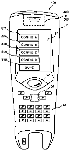
constant through the time the trigger signal remains active, and can be the
imaging assembly
of the imaging module having a longer best focus distance than remaining
imaging
assemblies of the module. When operating in Configuration H (still image
picture taking) or
Configuration I (motion video), terminal 100, in one embodiment, avoids
subjecting captured
frames of image data to decode attempts. Also, in an embodiment summarized in
Table 1,
terminal 100 can avoid energizing for energy conservation purposes light
source bank 1001
and light source bank 1002 when operating in accordance with Configuration I
or H (in some
embodiments, light from banks 1001, 1002 may have little effect when terminal
100 is
17
CA 02633437 2008-06-04
Attorney Docket No. H28277
PATENT
disposed at a substantial distance from a target while being used for picture
taking or motion
video).
[0055] Referring now to Table 2, a set of possible configurations for terminal
100 where
terminal 100 has or is utilizing a single image sensor is shown and described.
In the various
configurations shown in Table 2, terminal 100 is capable of varying imaging
attributes of
successively received frames by varying an illumination profile of terminal
100 between
frames.
[0056] When operating according to Configuration M, each frame received and
processed
by terminal 100 has a full illumination profile wherein each of light source
bank 1001 and
light source bank 1002 is energized during the exposure period corresponding
to each
received frame.
Table 2
FRAMES
CONFIGURATION
1 2 3 4 5 6 7 8 9 10
Illuminafion Illuminafion IlluminaBon Illuminafion Illumina6on Illumina6on
Illuminafion Illumina6on Illumina0on Illuminafion
M Profile Profile Profile Profile Profile Profile Profile Profile Profile
Profile
10010n 10010n 10010n 10010n 10010n 10010n 10010n 10010n 10010n 10010n
1002On 10020n 10020n 10020n 10020n 10020n 10020n 100200 10020n 10020n
Illuminabon Illuminafion Illuminafion Illuminafion Illuminafion Illuminabon
Illumination Illuminetion Illumina6on Illumina0on
N Profile Profile Profile Profile Profile Profile Profile Profile Profile
Profile
10010n 100108 10010n 100108 1001On 100108 10010n 10010(f 1001 On 1001Off
1002 OB 1002 On 1002 OB 1002 On 1002 08 1002 On 1002 0H 1002 On 1002 OB 1002
On
Illumination Illuminafion Illuminatlon Illuminabon Illuminabon Illumination
Illumination Illumina6on Illumina0on Illuminabon
0 Profile Profile Profile Profile Profile Profile Profile Profile Profile
Profile
10010n 1001On 10010n 100108 1001011 10010ft 10010n 10010n 10010n 100108
1002 08 1002 ON 100200 1002 0n 1002 0n 1002 0n 1002 011 1002 00 1002 OfF 1002
On
Illuminabon Illuminafion Illuminabon Illumina0on Illuminafion Illuminafion
Illuminafion Illuminafion Illuminafion Illumination
P Profile Profile Profile Profile Profile Profile Profile Profile Profile
Profile
10010n 10010n 1001 On 10010n 1001 On 1001 nff 1001 On 100108 10010n 1001 Off
1002 On 1002 On 1002 On 1002 On 1002 00 1002 0n 1002 00 1002 0n 1002 01f 1002
On
[0057] When operating according to Configuration N, terminal 100 alternates
between
receiving and processing frames having a first illumination profile and a
second illumination
profile wherein the first illumination profile is characterized by light
source bank 1001 being
energized during a corresponding exposure period and light source bank 1002
being de-
energized. The second illumination profile is characterized by light source
bank 1002 being
energized during a corresponding exposure period and light source bank 1001
being de-
energized. While operating in accordance with Configuration N, a likelihood of
specular
18
CA 02633437 2008-06-04
Attorney Docket No. H28277
PATENT
reflection read errors (including failures) can be expected to be reduced
relative to a
likelihood of read errors in Configuration M. Where terminal 100 is being held
at such
position that emitted light from one of light source bank 1001 or light source
bank 1002 is
being reflected substantially directly back at image sensor 311 to saturate
image sensor 311
operating in Configuration N assures that frames can be received that were
exposed during
exposure periods without the particular light source bank (1001 or 1002)
providing specularly
reflected light being energized. When operating in Configuration N or another
configuration
described herein when an attribute set is changed between frames, switching an
attribute set
between frames may not actually remove a saturated region (a grouping of pixel
locations
having peak or near peak pixel intensity values) from a frame that is received
and subject to
processing; but rather, may change the location of the saturated region.
Changing the
location of a saturated region may, nevertheless, render a decodable indicia
decodable in at
least two ways. For example, if the saturated region is moved to a location
away from a'
representation of decodable indicia, the decodable indicia may be rendered
decodable. Also,
if a saturated region is moved to a different location of a decodable indicia
representation in
the form of a certain type of bar code symbol, the symbol may be rendered
decodable by
combining a part of partial decoding results determined by attempting to
decode each of the
frames. An operator may select Configuration N where specular reflection
(saturation) read
conditions are expected to be encountered. Regarding Configuration 0,
Configuration 0 is
similar to Configuration N except than in Configuration 0, terminal 100
receives and
processes a plurality of frames having a first set of attributes prior to
receiving and processing
a plurality of frames having a second set of attributes.
[0058] Regarding Configuration P, Configuration P is similar to Configuration
N except
terminal 100 is adapted to receive a plurality of commonly attributed frames
prior to
switching to a mode in which a differently attributed frame is received. In
the example
described, frames 1-4 have common full illumination profiles. After frame 4,
the
illumination profiles are characterized by one or the other light source (but
not both) of
illumination light source banks being on during the frame's corresponding
exposure period.
[0059] When operating in Configuration P, terminal 100, after a trigger signal
is made
active can receive and process a predetermined number of frames having a "full
illumination"
(both light source banks 1001 and 1002 on) illumination profile and then if a
decoded
message is not determined prior to a time out period, can switch to a mode in
which terminal
19
CA 02633437 2008-06-04
Attorney Docket No. H28277
PATENT
100 alternately receives frames of image data having first and second
illumination profiles as
described in connection with the description of Configuration N. When
Configuration P is
made active, terminal 100 is adapted to decode under specular reflection read
error
(saturation) conditions but is provisioned so that terminal 100 processes
several frames
having a full illumination profile prior to switching operation into a mode
wherein different
light source banks 1001 and 1002 are selectively energized during subsequent
exposure
periods.
[0060] It has been described that terminal 100 can subject received frames to
decoding
processing. In subjecting a frame of image data to decoding processing,
terminal 100 can
attempt to decode a decodable indicia, e.g., a bar code symbol or an OCR
character. For
example, in attempting to decode a 1D bar code symbol represented in a frame
of image data,
processor 60 can execute the following processes. First, processor 60 can
launch a scan line
in a frame of image data, e.g., at a center of a frame, or a coordinate
location determined to
include a decodable indicia representation. Next, processor 60 can perform a
second.
derivative edge detection to detect edges. After completing edge detection,
processor 60 can
determine data indicating widths between edges. Processor 60 can then search
for start/stop
character element sequences and if found, derive element sequence characters
character by
character by comparing with a character set table. For certain symbologies,
processor 60 can
also perform a checksum computation. If processor 60 successfully determines
all characters
between a start/stop character sequence and successfully calculates a checksum
(if
applicable), processor 60 can output a decoded message. When outputting a
decoded
message, processor 60 can one or more of (a) initiate transfer of the decoded
message to an
external device, (b) initiate display of a decoded message on a display of
terminal 100, (c)
attach a flag to a buffered decoded message determined by processor 60, and
(d) write the
decoded message to an address on long term memory, e.g., 82 and/or 84. At the
time of
outputting a decoded message, processor 60 can send a signal to an acoustic
output device of
terminal 100 (not shown) to emit a beep.
[0061] In attempting to decode a decodable symbol, terminal 100 can, in some
cases,
determine a set of code words of a bar code symbol. Code words of a bar code
symbol are
not complete decoded messages of a bar code symbol but can be combined with
other code
words of a bar code symbol to provide a complete decoded message. A decoded
code word
of a bar code symbol may be regarded as a partially decoded message.
Symbologies which
CA 02633437 2008-06-04
Attorney Docket No. H28277
PATENT
may be decoded to provide code words representing a partial decoded message of
a bar code
symbol include PDF 417, UPC, Datamatrix, QR code, and Aztec, etc.
[0062] In decoding certain symbologies, terminal 100 can be adapted to combine
partial
decoded out results determined from two or more different frames. A partial
decode result
provided by decoding a frame of image data can take the form of a set of code
words.
Terminal 100 can be adapted to determine a first set of code words by
processing a certain
frame of a set of frames received while a trigger signal is active and to
combine the first set
of code words with a second set of code words determined by processing of a
subsequent
frame while the trigger signal remains active. In one embodiment, terminal 100
can be
adapted so that terminal 100 can process a certain frame to determine a first
set of code
words, a subsequent frame to provide a second set of code words, and a further
subsequent
frame to provide a third set of code words. Terminal 100 can further be
adapted to combine
the first, second, and third set of code words to provide a decoded message.
For example,
with reference to a configuration described with reference to Table 1 or 2,
terminal 100 may
process frame 1 to determine a first set of code words and then process frame
2 to determine
a second set of code words and then combine the code words to provide a
decoded message.
[0063] Regarding the terms "certain frame," "subsequent frame," and "further
subsequent
frame," frames 1, 2, and 3 in any of the Configurations described in Tables 1
and 2 are
examples of "certain subsequent" and "further subsequent frames." Frames 1, 4
and 9 are
also examples of frames that may be designated as a "certain frame,"
"subsequent frame,"
and a "further subsequent frame," as well as frames 2, 3 and 7 and so forth.
[0064] For further describing operation of terminal 100 in one embodiment,
Figs. 12 and
13 describe exemplary certain and subsequent frames of image data that may be
received and
subjected to processing by terminal 100. Fig. 12 shows exemplary certain and
subsequent
frames where the frames have different source imaging attributes, and possibly
different
illumination profile imaging attributes. It is seen that the subsequent frame
of Fig. 12 may
have a larger field of view than the certain frame and accordingly
representation 1011 therein
of a certain indicia may be represented with a smaller percentage of frame
pixel values than
the representation 1010 of the certain indicia in the certain frame. It is
further seen with
reference to Fig. 12 that while the certain frame may have a saturation region
1012
preventing decoding representation 1010 corresponding to the certain indicia,
the subsequent
frame may be devoid of a saturation region. With the certain frame having
saturation region
21
CA 02633437 2008-06-04
Attorney Docket No. H28277
PATENT
1012 coincident with the indicia representation 1010 and with the subsequent
frame being
devoid of a saturation region, a subjecting of the certain frame to a decode
attempt may result
in a determination that the indicia corresponding to representation 1010
cannot be decoded
and a subjecting of the subsequent frame to a decode attempt may result in a
successful
decode (a decoded message corresponding to the certain indicia being
determined and
output).
[0065] Fig. 13 shows exemplary certain and subsequent frames where the frames
have
different illumination profiles but a common source attribute. The frames have
common
source and accordingly as expected, the indicia representations 1020, 1021 of
the frames
corresponding to a certain decodable indicia have substantially the same size
and position
between the certain and subsequent frames. Regarding the certain frame, the
certain frame
has a saturation region 1022 coincident with a first part of representation
1020 representing a
first part of a certain indicia. Regarding the subsequent frame, the
subsequent frame also has
a saturation region 1024; however, the position of the saturation region is
shifted relative to
the position of saturation region 1022 as a result of the different
illumination profile of the
subsequent frame. Regarding representation 1020, representation 1020 can be
subject to a
decoding processing decode attempt to provide a first set of code words
representing a partial
decoding result and representation 1021 of a subsequent frame can be subject
to a decoding
processing decode attempt to determine a second set of code words also
representing a partial
decoding result. Terminal 100 can combine the first set of code words and the
second set of
code words to provide a decoded message corresponding to the indicia commonly
represented by representation 1020 and representation 1021 of the certain and
subsequent
frames.
[0066] Terminal components illustrated in Figs. 10 and 11 can be incorporated
in and
supported by a hand held housing. An exemplary hand held housing for
supporting terminal
components is shown and described in Fig. 14 and Fig. 15. As seen in Fig. 15,
a plurality of
circuit boards 402 including motherboard 1402 can be supported on struts 404
extending
from interior walls of housing 11. An imaging module such as imaging module
400 or 500
can be incorporated in and can be supported by housing 11, specifically by
supports 406
extending from an interior wall of housing 11. As indicated, terminal 100 can
be adapted so
that the configurations described in Table 1 and Table 2 are manually user
selectable. For
example, terminal 100 can include graphical user interface displays buttons
802, 804, 806,
22
CA 02633437 2008-06-04
Attorney Docket No. H28277
PATENT
808 corresponding to several of the configuration options ("more" button 810
can be actuated
to access additional buttons corresponding to additional configurations). An
operator can
manually select a designated configuration by actuating (e.g., "clicking on")
a button
corresponding to the desired configuration. In Fig. 14, display 97 is shown as
displaying
Configurations A-D. Terminal 100 can be adapted to display buttons
corresponding to any
configuration described herein, including those described in Table 1 and Table
2.
[0067] Referring now to further aspects of imaging module 400 and imaging
module 500,
imaging module 400 and imaging module 500 can be prepackaged imaging modules,
meaning that they are entirely or substantially entirely assembled into the
form shown in
Figs. 2 and 5, respectively prior to being installed into a terminal housing
such as housing 11
(Figs. 14, 15). When in an assembled form as shown in Figs. 2 and 5,
components of
imaging module 400, 500 are held in a certain position relative to one
another.
[0068] In one aspect of a plural image sensor imaging module, imaging module,
e.g.,
module 400 can be adapted to emulate the controllability and output
characteristics of an
imaging module e.g., module 500 having a single image sensor. For example, as
will be
described further herein imaging module 400 can have a certain number of image
data output
contacts forming a set of image data contacts and image data corresponding to
any one of the
image sensors (e.g., image sensors 111, 211) of the imaging module can be
output through
the set of image data contacts. In one embodiment, a plural image sensor
imaging module
can be provided having a plurality of image sensors and a single set of video
contacts
provided for purposes of asynchronously transmitting image data corresponding
to image
systems generated by each of the image sensors.
[0069] In another aspect, a kit can be provided having a multiple module
supporting
image capture and processing circuit that is adapted to capture and process
image data
corresponding to image signals generated by either one of plural image sensor
imaging
module, e.g., module 400 or a single image sensor imaging module 500. That is,
either one
of imaging module 400 or 500 can be connected to a specifically adapted image
capture and
processing circuit and the specifically adapted image capture and processing
circuit can
receive and process corresponding image signals to generate image data from
the connected
module. A kit can further include a specifically adapted plural image sensor
imaging module
and a particularly adapted single image sensor imaging module which are
specifically
23
CA 02633437 2008-06-04
Attorney Docket No. H28277
PATENT
adapted so that the specifically adapted image capture and processing circuit
can receive and
process image data corresponding to image signals generated by either the
plural image
sensor imaging module or the single image sensor imaging module. Such a kit
can be
utilized by manufacturers of indicia reading terminals (including integrator
manufacturers)
for the manufacture of bar code and other types of indicia reading terminals.
[0070] , A representation of a kit for use by manufacturers of indicia reading
terminals is
shown in Fig. 16. Kit 1500 can comprise a multiple module image capture and
processing
circuit 1510 disposed on a common circuit board 1402 (which can be referred to
as a
motherboard), a set of candidate plural image sensor imaging modules 400, 401
and a set of
candidate single image sensor imaging modules 500, 501. In use, one of imaging
modules
400, 401, 500, 501 can be connected to motherboard 1402 that carries image
capture and
processing circuit 1510. In one embodiment, any one of imaging modules 400,
401, 500, 501
can be connected to motherboard 1402, carrying image capture and processing
circuit 1510,
through a flex connector 1520. It can be seen that kit 1500 can advantageously
reduce
manufacturing and maintenance costs for indicia reading terminal 100. For
example suppose
a customer orders S plural module indicia reading terminals and T single image
sensor indicia
reading terminals. If a custom made image capture and processing circuit were
provided for
each module type, the manufacturer would have to provide S image capture and
processing
circuits for use with the plural image sensor module and T image capture and
processing
circuits for use with the single image sensor module. The manufacturer would
therefore have
to design and manufacture two different image capture and processing circuits.
With use of
kit 1500 design costs can be reduced since only one not two image capture and
processing
circuits are provided. With use of kit 1500, the customer order can be filled
by
manufacturing S+T like manufactured image capture and processing circuits.
Given
principles of economies of scale, the manufacturing costs associated with
providing S+T
commonly manufactured units can be expected to be less than the costs
associated with the
manufacture of S first units and T second units.
[0071] Further aspects of kit 1500 and of a plural image sensor imaging module
400 for
use with kit 1500 are described with reference to Fig. 17, where the
components of module
400 can function in accordance with the corresponding components shown and
described in
connection with Fig. 10 and where the components of image capture and
processing circuit
24
CA 02633437 2008-06-04
Attorney Docket No. H28277
PATENT
1510 can function in the manner of the corresponding components shown and
described in
connection with the circuits of Figs. 10 and 11. While the kit depicted in
Fig. 17 is shown in
assembled form as having image module 400 connected to image capture
processing circuit
1510, it is understood that another imaging module type such as module 401,
500 (having the
components of and functioning in the manner described in connection with Fig.
11), or
module 501 could be connected to image capture and processing circuit 1510. In
one
example, the various types of imaging modules 400, 401, 500, 501 can be
differentiated in
terms of the characteristics of the imaging assembly or assemblies
incorporated therein. For
example, imaging module.400 can have imaging assemblies according to
Embodiment A of
Table A, and imaging module 401 can have imaging assemblies according to
Embodiment B
(or; alternatingly C, or D, or E, or F) of Table A. Imaging module 500 can
have a two
dimensional image sensor and a first fixed best focus distance, while imaging
module 501
can have a linear image sensor and a second fixed best focus distance.
[0072] Fig. 17 shows a specific embodiment of a terminal circuit having a
plural image
sensor imaging module 400 adapted to be in communication with a multi-module
image
capture and processing circuit 1510 which is adapted to receive many different
alternative
candidates and modules which can be of a variety of different embodiments
(types). In the
specific embodiment of Fig. 16 image capture and processing circuit 1510 can
be adapted to
receive plural image sensor imaging modules of any of the embodiments
summarized in
Table A as well as several embodiments of single image sensor imaging modules.
Image
capture and processing circuit 1510 can be adapted so that the components of
image capture
and processing circuit 1510 function in the manner of the corresponding
components
described in connection with the circuits shown in Figs. 10 and 11. For
example, image
capture and processing circuit 1510 can be adapted so that frames of image
data can be
received into RAM 80, and further so that processor 60 can address such frames
for
subjecting such frames to decoding (e.g., bar code decoding for attempting to
decode a bar
code) processing.
[0073] For supporting multiple imaging modules, resources such as software
resources
can be incorporated into image capture and processing circuit 1510. Software
resources for
supporting multiple alternative imaging modules can be suitably stored in non-
volatile
memory 82. For example, first resources can be provided for supporting a first
embodiment
CA 02633437 2008-06-04
Attorney Docket No. H28277
PATENT
(type) of plural image sensor imaging module, second resources can be provided
for
supporting a second embodiment (type) of a plural image sensor imaging module,
third
resources can be provided for supporting a first embodiment (type) of a single
image sensor
imaging module fourth resources can be provided for supporting a second
embodiment (type)
of a single image sensor imaging module and so on. Further, each imaging
module 400, 401,
500, 501 can have a memory storing identifying information for the imaging
module.
Identifying information in one embodiment can be a memory stored serial number
for an
imaging module in one embodiment. In another embodiment, identifying
information for an
imaging module, e.g., module 400, 401, 500, 501 can be a set of two wire
interface addresses
for integrated circuits of an imaging module 400, 401, 500, 501. Each
integrated circuit of an
imaging module that is in communication with two wire interface bus 1540 can
be assigned a
different two wire interface address for use in communicating with the
integrated circuit.
Processor 60 of image capture and processing circuit 1510 can be configured to
execute a
command wherein processor 60 reads the two wire interface addresses of all
integrated
circuits of a connected imaging module e.g., 400, 401, 500, 501 and determines
the type of
the connected module based on the returned address information. In another
embodiment,
identifying information for an imaging module can be image data output by the
imaging
module which can be processed by an image capture and processing circuit for
determining
an identity of a connected image sensor (each candidate imaging module can be
expected to
output image data having unique characteristics detectable with use of image
capture and
processing circuit 1510). Kit 1500 can be provided so that when a specific
imaging module
(which may be plural image sensor or single image sensor) is connected to
image capture and
processing circuit 1510 (e.g., by connecting the module to a ribbon connector
connected to
the image capture and processing circuit 1510) the image capture and
processing circuit 1510
responsively to a module being connected to the image capture and processing
circuit 1510,
reads the identifying information and responsively activates the appropriate
resources (e.g.,
first, second, third, or fourth) depending on which type of imaging module has
been
connected. The resources associated with each imaging module can determine,
e.g., the
available configurations associated with each module, and the behavior of the
imaging
module when operating in accordance with a particular configuration. Kit 1500
can also be
adapted so that image capture and processing circuit 1510 reads identifying
information and
responsively activates appropriate resources in response to receipt of a user
initiated
command input by using a user interface.
26
CA 02633437 2008-06-04
Attorney Docket No. H28277
PATENT
[0074] Aspects of specific examples of a kit for use in manufacturing indicia
reading
terminals are now further described. In one embodiment, as is indicated in
Fig. 18, terminal
100 can be constructed so that dual DMA channels 70 and 70' and dual
processors 60 and 60'
are provided for capture and processing of image data corresponding to image
signals
generated by image sensor 111 and image sensor 211. In the embodiment of Fig.
18, a
common two wire interface bus 1540 is provided for use by processor 60 and
processor 60'.
Processor 60 can utilize bus 1540 for sending imaging commands and parameter
data to
image sensor 111, while processor 60' can utilize common bus 1540 for sending
imaging
commands and parameter data to image sensor 211.
[0075] In the embodiment of Fig. 17 circuit 1510 of reduced cost can be
provided so that
a single DMA channel 70 is provided for capture of image data corresponding to
image
signals generated by each of image sensor 111 and image sensor 211. The
connected
imaging module 400 of Fig. 17 is shown as having a multiplexer 72 receiving
image data
representing light incident on a first image sensor 111 or a second image
sensor 211 as
described e.g., in connection with Fig. 10. As will be described herein,
multiplexer 72 can
output image data for transmission through a set of video contacts. As
indicated by dashed-in
border 1530, DMA unit 70 and processor 60 can be integrated onto a common
processor IC
chip having DMA functionality. DMA unit 70 can also be provided by a dedicated
hardware
element e.g., a field programmable gate array (FPGA) or an application
specific integrated
circuit (ASIC). A processor IC chip having DMA functionality can have an
associated buffer
68, facilitating receipt of asynchronously clocked image data clocked
asynchronously relative
to a master clock of the processor IC chip designated by dashed-in border
1530. One
commercially available integrated circuit chip having integrated DMA
functionality is the
XSCALE PXA27X microprocessor available from Intel, Inc. Another commercially
available integrated circuit chip having integrated DMA functionality is the
FREESCALE
MC9328MXL microprocessor available from Freescale Semiconductor, Inc.
[0076] For feeding image data corresponding to image signals generated by each
of
image sensor 111 and image sensor 211 into the single DMA unit 70, imaging
module 400
can have a connector port 1536. Connector port 1536 can have a plurality of
electrical
contacts e.g., contacts C00-C31 (contacts). In one embodiment, connector port
1536 can be a
27
CA 02633437 2008-06-04
Attorney Docket No. H28277
PATENT
ribbon connector port having a plurality of contacts for detachably receiving
a ribbon
connector 1520. In another embodiment, connector port 1536 can be a pin
connector or a
hole connector of a pin and hole type connector port. Connector port 1536 in
one
embodiment can have a plurality of contacts COO through C31 for transmission
of image data
corresponding to image signals generated by both of image sensor 111 and image
sensor 211,
and for transmission of various control and handshaking signals between
imaging module
400 and image capture and processing circuit 1510. Connector port 1536 as
shown in the
embodiments of Fig. 5, Fig. 9, Fig. 16, is shown as being mounted to an
imaging module
circuit board carrying one or more image sensors and therefore is shown as
being held in a
certain position relative to one or more image sensors. In another embodiment,
connector
port 1536 can be tethered, e.g., via a flex connector to a major body of an
imaging module.
In another embodiment, connector port 1536 in any of the embodiments shown,
can be
deleted and substituted for by an exposed set of electrical contacts.
Circuitry e.g., image
capture and processing circuit 1510 can be connected to an imaging module
having an
exposed set of electrical contacts by soldering to electrical leads to the
exposed set of
electrical contacts.
[0077] A contact layout of an imaging module in one embodiment is summarized
in
Table 3, wherein a number of contacts are provided by contacts enumerated COO -
C3 1.
Contacts as summarized in Table 3 can be e.g., contacts of connector port 1536
or exposed
contacts of an imaging module for soldering to external circuitry.
28
CA 02633437 2008-06-04
Attorney Docket No. H28277
PATENT
Table 3
CONTACT ASSIGNMENT
C00 Ground
CO1 Power
C02 Video
C03 Video
C04 Video
C05 Video
C06 Video
C07 Video
C08 Video
C09 Video
C10 Video
C 11 Video
C12 HSYNC
C13 VSYN
C14 PLCK
C15 Reset
C16 Standby
C17 SDA
C18 SCL
C19
C20
C21
C22
C23
C24
C25
C26
C27
C28
C29
C30
C31
[0078] Regarding the assignment of contacts C00-C31 contacts C02-C011 can be
assigned for carrying image data. For example, if the image data is 10 bit
image data ten (10)
image data contacts (designated "video" contacts in Table 3) can be provided.
If the image
29
CA 02633437 2008-06-04
Attorney Docket No. H28277
PATENT
data is 8 bit image data eight (8) image data contacts can be provided.
Regarding additional
contact assignments of connector port 1536, contact COl can be a.power/enable
contact for
delivering power to imaging module 400 from motherboard 1402, contact COO can
be a
ground contact for carrying a ground path to imaging module 400, and contact
C15 can be a
reset contact for transmitting a reset signal. A reset signal can be
transmitted over contact
C15 to a set of integrated circuits, e.g., integrated circuits 111, 211, 72 of
a connected
imaging module into a reset state. Further, contact C 16 can be a standby
contact. A standby
signal can be transmitted over contact C16 to set integrated circuits, e.g.,
integrated circuits
111, 211, 72, into a standby (low power) state. Referring to contact C12,
contact C13 and
contact C 14, contacts C 12, C 13, C 14 can be contacts for carrying
horizontal (row)
synchronization signals (HSYNC), vertical (frame) synchronization signals
(VSYNC) and
pixel clock (PLCK) signals from image sensor 111 and from image sensor 211.
Such signals
can be received by DMA unit 70 and can be received by camera interface buffer
68 which is
interfaced to DMA unit 70. Row synchronization, frame synchronization, and
pixel clock
signals can be performing timing operations so that frames of image data are
appropriately
written into memory 80 where frames can be addressed for further processing by
processor
60. In one embodiment, a master clock signal can be delivered from processor
integrated
circuit 1530 to imaging module 400. However, in another embodiment, as is
indicated by
imaging module clock 1533, imaging module 400 and image capture and processing
circuit
1510 can have asynchronous clocks.
[0079] Further regarding connector port 1536, connector port 1536 is shown as
including
a single power signal contact CO1. In other embodiments, connector port 1536
can have
additional power signal contacts. For example, where light source banks 1001,
1002, 1003,
1004 might consume substantial power, additional illumination power signal
lead lines might
be provided to avoid noise coupling between illumination image sensor and
power lead lines.
Additional power signal contacts can also reduce a voltage drop across a
connector, e.g., a
flex strip connector connecting image capture and processing circuit 1510 and
an imaging
module, e.g., imaging module 400.
[0080] Contacts C00-C31 can also include two wire interface (TWI) contacts
that form
part of a command carrying digital bus such as two wire interface bus 1540. It
is seen that
the circuit of Fig. 17 including the combined circuitry of imaging module 400
and image
CA 02633437 2008-06-04
Attorney Docket No. H28277
PATENT
capture and processing circuit 1510 can include a two wire interface bus 1540
partially
disposed on imaging module and partially disposed on spaced apart image
capture and
processing circuit 1510 that enables processor 60 to send. commands to various
integrated
circuits of imaging module 400. In one example, two wire interface bus 1540
includes signal
line 1540a (SDA line) for transmitting data and clocking signal line 1540b
(SCL line) for
transmitting a clocking signal. In the example of Table 3, contact C17 forms
part of the data
signal line and contact C18 forms part of the clocking signal line. Data
signal line 1540a can
carry address information commands (e.g., exposure, gain, output enable,
output disable) and
parameters (exposure values, gain values). In the example of Fig. 17, the data
signal line
contact and clocking signal signal line contact can be interfaced to TWI bus
signal lines of
ribbon connector 1520 which in turn are connected to TWI bus signal lines of
connector port
1546 of motherboard 1402 which in turn are interfaced to the portion of TWI
bus 1540 on
motherboard 1402. In one embodiment, two wire interface bus 1540 is provided
by a
PHILLIPS 12C bus.
[0081] Various integrated circuits of imaging module 400; namely, image sensor
111,
image sensor 211, and MUX 72 (provided in the specific embodiment by a field
programmable gate array (FPGA)) can be adapted to interpret and execute the
commands
sent on data signal line 1540a. For controlling image sensor 111 and image
sensor 211 in a
coordinated manner, processor 60 can send various commands on two wire
interface bus
1540. On data signal line 1540a there can be time divided address data,
commands, and
parameter data, the address data indicating which of the integrated circuits
of imaging module
400 will interpret the command. On clock signal line 1540b there are
transmitted clocking
signals. For providing a single two wire interface bus 1540 that supports and
which can
transmit commands to a plurality of integrated circuits, e.g., image sensor
integrated circuits
111 and 211, each integrated circuit can be assigned a different two wire
interface address so
that commands and/or parameter data intended for a specific integrated circuit
can be sent to
a specific integrated circuit. The manner in which processor 60 can send
commands over two
wire interface bus 1540 depends on which configuration, e.g., a configuration
as summarized
in Table 1 has been made active. Serially transmitted commands that can be
transmitted on
signal line 1540a can be, e.g., image sensor enable commands, image sensor
disable
commands, exposure commands, gain commands, address data commands (commands).
Parameter data transmitted on data signal line 1540a can be serially
transmitted data.
31
CA 02633437 2008-06-04
Attorney Docket No. H28277
PATENT
[0082] For example, for Configuration C of Table 1 wherein frames from two
different
imaging assemblies can be captured and subject to decoding processing the
following set of
commands, summarized in Table 4 can be initiated by processor 60 and
transmitted through
two wire interface 1540.
Table 4
{
if (SENSOR1_frame)
{
compute newEXP(Sensorl, &nExposurel);
compute newGAIN(Sensor1, &nGainl);
SENSOR.WritelIC(SENSOR1_EXPOSURE_REG,&nExposure1,1);
SENSOR.WritelIC(SENSOR1_ANALOG_GAIN_REG,&nGain1,1);
}
if (SENSOR2_frame)
{
compute newEXP(Sensor2,&nExposure2);
compute newGAIN(Sensor2,&nGain2);
SENSOR.WritelIC(SENSOR2_EXPOSURE_REG,&nExposure2,1);
SENSOR.WritelIC(SENSOR2_ANALOG_GAIN_REG,&nGain2,1);
}
}
[0083] Further regarding the circuit diagram of Fig. 17, two wire interface
bus 1540 can
also be coupled to regulators 74, 76, 174, 176. As noted, regulators 74, 76,
174, 176 can be
adapted to deliver power to light source banks 1001, 1002 and aiming light
source banks
1003, 1004. Coupling two wire interface bus 1540 to regulators 74, 76, 174,
176 enables
light source bank control commands to be transmitted through bus 1540 for
interpretation and
execution by regulators 74, 76, 174, 176, all of which can be equipped with
registers and
microcontrollers for receiving and executing light source bank control
commands.
Additionally a frame synchronization signal (e.g., a VSYNC signal) output by
image sensor
111 and image sensor 211 can be input to regulators 74, 76, 174, 176 so that
operation of
light source banks 1001, 1002 and aiming light source banks 1003, 1004 can be
appropriately
synchronized with the operation of image sensors 111, 211. Also, an exposure
output signal
output from image sensor 111, 211 can be input to regulators 74, 76, 174, 176
for
synchronization between image sensors 111, 211 and light source banks 1001,
1002, 1003,
1004. In a further aspect, imaging module 400 can include a dedicated imaging
module clock
1533 which operates separately and asynchronously relative to a master clock
of a processor
integrated circuit designated by dashed-in border1530. As indicated in the
circuit diagram of
Fig. 17, a clocking signal can be interfaced to image sensor 111, image sensor
211, and
32
CA 02633437 2008-06-04
Attorney Docket No. H28277
PATENT
multiplexer 72. Providing a dedicated imaging module clock 1533 alleviates a
need to
transmit a master clocking signal from image capture and processing circuit
1510 and hence,
alleviates a need to provide an additional signal line in a connector, e.g.,
connector 1520
connecting imaging module 400 and image capture and processing circuit 1510.
[0084] As the number of signal lines of connector port 1536 increase it can be
expected
that electromagnetic interference radiation (EMI) radiating from the signal
lines of ribbon
connector 1520 can increase. Where terminal 100, as shown in the embodiment of
Fig. 18
incorporates a sufficient number of signal lines for simultaneously carrying
image data
corresponding to image sensor 111 and image sensor 211 the EMI radiation level
for
connector 1520 can be expected to be relatively higher than for the embodiment
where the
connector 1520 has sufficient signal lines for alternatingly transmitting
image data
corresponding to image signals generated by image sensor 111 and image sensor
211.
Further, where an imaging module includes one image sensor (as shown in Fig.
19) or a
plurality of image sensors the EMI radiation level can be expected to be
increased as the
resolution of the image sensor image data increases (e.g., from 8 bit
requiring 8 data signal
lines, to 10 bit to 16 bit to 32 bit). [0085] A circuit limiting the amount of
EMI radiation radiating from a connector
connecting terminal imaging module 400 to an image processing circuit 1510 is
described
with reference to Fig. 20. As shown in Fig. 15, an imaging module 400, 401,
500, 501 can be
spaced apart from a motherboard 1402 which carries image capture and
processing circuit
1510. In the embodiment of Fig. 20, an imaging module 400 or 500 having the
components
generally described with reference to the embodiment of Fig. 20 (circuit 1702
of Fig. 20
represents the components within dashed border 1702 of Fig. 17 or
alternatively the
components within dashed border 1702 of Fig. 18 or alternatively, the
components within
dashed border 1702 of Fig. 19) can include a parallel to serial converter 1710
and an image
capture and processing circuit 1510 of terminal 100 can include a serial to
parallel converter
1712 which is interfaced to circuit 1704 representing the components within
dashed-in border
1704 of Fig. 17 or alternatively the components within dashed-in border 1704
of Fig. 18 or
alternatively the components within dashed-in border 1704 of Fig. 19. Parallel
to serial
connector 1710 can receive for conversion a plurality of input data signals,
input in parallel.
Such parallel input data signals can include data signals forming multi-bit
image data values.
Shown as being a component separate from image sensors 111, 211 parallel to
serial,
33
CA 02633437 2008-06-04
Attorney Docket No. H28277
PATENT
converter 1710 can be incorporated into an integrated circuit forming image
sensor 111, 211,
311 (of a single image sensor imaging module). Between converter 1710 and
converter 1712
there can be provided a complementary differential pair interface connector
1716 having a
pair of signal lines transmitting a differential pair of signals. Differential
pair connector 1716
can be connected to differential pair connector port 1711 which receives an
output from
parallel to serial converter 1710 and differential pair connector port 1713
which transfers
differential pair signals to serial to parallel converter 1712. Converter 1710
and converter
1712 can be complementarily adapted so that converter 1712 can process the
received signal
from the differential pair to recover the parallel input data signals input to
converter 1710.
Providing converters 1710, 1712 and connector 1716 can greatly reduce the
number of signal
lines between an imaging module, e.g., imaging module 400, 401, 500, 501, and
an image
capture and processing circuit 1510. Connector 1716 can be provided, e.g., by
a set of
twisted pair signal lines, a Twinax cable, or a set of closely coupled
differential traces of a
flex circuit. Accordingly, a set of differential pair signal lines can be
integrated into ribbon
connector 1520. In another embodiment adapted so that EMI emissions are
reduced, parallel
to serial converter 1710 can be a converter adapted to convert parallel input
data signals to
into a serially output optical signal output by converter 1710 to connector
1716, and
converter 1712 can be a converter adapted to process received serially
transmitted optical
signals to recover the set of parallel data signals received at converter
1710. Connector 1716
in such an embodiment can be a fiber optic cable adapted to transmit a
serially output optical
signal output by parallel to serial converter 1710. Parallel to serial
converter 1710 can be
disposed on an imaging module. For example, one or more circuits forming
parallel to serial
converter 1710 can be mounted to circuit board 402 (Fig. 5) in an example of a
plural image
sensor imaging module or circuit board 502 (Fig. 9) in an example of a single
image sensor
imaging module.
[0086] A small sample of the methods of an apparatus described herein are as
follows.
Al. A hand held indicia reading terminal for reading a decodable indicia
disposed on a
substrate, said hand held indicia reading terminal comprising:
an imaging assembly comprising an image sensor generating image signals and an
imaging lens focusing an image onto an active surface of said image sensor,
the imaging
assembly having a field of view defined on said substrate when an imaging axis
of said
imaging assembly is directed toward said substrate;
34
CA 02633437 2008-06-04
Attorney Docket No. H28277
PATENT
a working memory receiving image data corresponding to said image signals;
a first illumination assembly having a first light source bank directing light
toward
said field of view;
a second illumination assembly having a second light source bank directing
light
toward said field of view;
wherein said terminal is adapted so that when a trigger signal is active said
terminal
receives into said working memory a certain and a subsequent frame of image
data, wherein
each of the certain and subsequent frames has a corresponding exposure period,
wherein said
first frame of image data has a first illumination profile and said subsequent
frame of image
data has a second illumination profile, the first illumination profile being
different than said
second illumination profile, the first illumination profile being
characterized by said first light
source bank being ON and said second light source bank being OFF during said
exposure
period corresponding to said certain frame, said second illumination profile
being
characterized by said first light source bank being OFF and said second light
source bank
being ON during said exposure period corresponding to said subsequent frame of
image data;
wherein said terminal is adapted so that said terminal can process said
certain frame
of image data to determine a first set of code words, process said subsequent
frame of image
data to determine said second set of code words and combine said first and
second set of code
words.
B l. A hand held indicia reading terminal for reading a decodable indicia
disposed on a
substrate, said hand held indicia reading terminal comprising:
an imaging assembly comprising an image sensor generating image signals and an
imaging lens focusing an image onto an active surface of said image sensor,
the imaging
assembly having a field of view defined on said substrate when an imaging axis
of said
imaging assembly is directed toward said substrate;
a working memory receiving image data corresponding to said image signals;
a first illumination assembly having a first light source bank directing light
toward
said field of view;
a second illumination assembly having a second light source bank directing
light
toward said field of view;
a trigger button;
CA 02633437 2008-06-04
Attorney Docket No. H28277
PATENT
wherein said terminal is adapted so that when a trigger signal is active said
terminal
operates in a first mode until a timeout period has expired and then switches
to a second
mode, wherein said terminal is adapted so that said timeout period is
satisfied conditionally
on the condition that said terminal does not determine a decoded message
corresponding to
said decodable indicia prior to said timeout period;
wherein said terminal in said first mode receives into said working memory for
decoding processing a plurality of frames, each frame subject to decoding
processing in said
first mode having a common illumination profile;
wherein said terminal in said second mode varies an illumination profile of
received
frames received for decoding processing in such manner that in said second
mode said
terminal receives into a said working memory a certain and a subsequent frame
of image
data, wherein each of the certain and subsequent frames has a corresponding
exposure period,
wherein said first frame of image data has a first illumination profile and
said subsequent
frame of image data has a second illumination profile, the first illumination
profile being
different than said second illumination profile, the first illumination
profile being
characterized by said first light source bank being ON and said second light
source bank
being OFF during said exposure period corresponding to said certain frame,
said second
illumination profile being characterized by said first light source bank being
OFF and said
second light source bank being ON during said exposure period corresponding to
said
subsequent frame of image data;
wherein said terminal is adapted to subject to decoding processing each of
said certain
and subsequent frames of image data received in said second mode.
Cl. A hand held indicia reading terminal for reading a decodable indicia
disposed on a
substrate, said hand held indicia reading terminal comprising:
a first imaging assembly comprising a first image sensor generating image
signals and
an imaging lens focusing an image onto an active surface of said first image
sensor, the
imaging assembly having a first field of view defined on said substrate when
an imaging axis
of said first imaging assembly is directed toward said substrate;
a second imaging assembly comprising a second image sensor generating image
signals and an imaging lens focusing an image onto an active surface of said
second image
sensor, the imaging assembly having second field of view defined on said
substrate
36
CA 02633437 2008-06-04
Attorney Docket No. H28277
PATENT
overlapping said first field of view when an imaging axis of said second
imaging assembly is
directed toward said substrate;
a working memory, wherein said terminal is adapted so that said terminal can
receive
image data corresponding to image signals generated either by said first image
sensor or said
second image sensor into said working memory;
a first illumination assembly having a first light source bank directing light
toward
said first and second fields of view;
a second illumination assembly having a second light source bank directing
light
toward said first and second fields of view;
wherein said terminal is adapted so that when a trigger signal is active said
terminal
receives into a said working memory for decoding processing a certain and a
subsequent
frame of image data, wherein each of the certain and subsequent frames has a
corresponding
exposure period, wherein said certain frame of image data has a first set of
imaging attributes
and said subsequent frame of image data has a second set of imaging
attributes;
wherein said first set of imaging attributes are characterized by the
following: said
first light source bank is OFF during said exposure period corresponding to
said certain
frame; said second light source bank is ON during said exposure period
corresponding to said
certain frame, and said certain frame of image data comprises image data
corresponding to
image signals generated by said first image sensor; and
wherein said second set of imaging attributes are characterized by the
following: said
first light source bank is ON during said exposure period corresponding to
said subsequent
frame; said second light source bank is OFF during said exposure period
corresponding to
said subsequent frame, and said subsequent frame of image data comprises image
data
corresponding to image signals generated by said second image sensor.
C2. The hand held indicia reading terminal of claim C 1 wherein said first
imaging
assembly and said second imaging assembly have different fixed best focus
distances.
C3. The hand held indicia reading terminal of claim C1, wherein one of said
first and
second image sensors is a monochrome image sensor and a remaining of said
first and second
image sensors is a color image sensor.
37
CA 02633437 2008-06-04
Attorney Docket No. H28277
PATENT
C4. The hand held indicia reading terminal of claim C1, wherein one of said
first and
second image sensors is a linear image sensor and a remaining of said first
and second image
sensors is a two dimensional image sensor.
C5. The hand held indicia reading terminal of claim C1, wherein one of said
first and
second image sensors is a linear monochrome image sensor and a remaining of
said first and
second image sensors is a two dimensional color image sensor.
D1. A hand held indicia reading terminal for reading a decodable indicia
disposed on a
substrate, said hand held indicia reading terminal comprising:
a printed circuit board;
a first imaging assembly comprising a first image sensor generating image
signals and
an imaging lens focusing an image onto an active surface of said first image
sensor, the
imaging assembly having a first field of view defined on said substrate when
an imaging axis
of said imaging assembly is directed toward said substrate, said first image
sensor being
provided by a first integrated circuit chip, said first integrated circuit
chip being mounted to
said printed circuit board;
a second imaging assembly comprising a second image sensor generating image
signals and an imaging lens focusing an image onto an active surface of said
second image
sensor, the imaging assembly having second field of view defined on said
substrate
overlapping said first field of view when an imaging axis of said imaging
assembly is
directed toward said substrate, said second image sensor being provided by a
second
integrated circuit chip, said second integrated circuit chip being mounted to
said printed
circuit board, said printed circuit board being a single printed circuit board
commonly
carrying said first integrated circuit chip and said second integrated circuit
chip; and
a first configuration and a second configuration, the terminal being adapted
so that an
operator can manually select said first configuration and can further manually
select said
second configuration, wherein said terminal when said first configuration is
active operates
according to said first configuration, the terminal further being adapted so
that when said
second configuration is active said terminal operates in accordance with said
second
configuration;
wherein said terminal is adapted so that when a trigger signal and said first
configuration and said trigger signal are active, said terminal receives into
said working
38
CA 02633437 2008-06-04
Attorney Docket No. H28277
PATENT
memory for decoding processing a plurality of frames of image data, each of
said plurality of
frames of image data representing light incident on a select one of said first
image sensor and
said second image sensor, wherein said terminal does not receive into said
working memory
for decoding processing frames of image data representing light incident on an
image sensor
other than said select one of said first image sensor and said second image
sensor when said
first configuration is active;
wherein said terminal is further adapted so that when said second
configuration and a
trigger signal are active, said terminal receives into said working memory for
decoding
processing a certain and a subsequent frame of image data, wherein each of the
certain and '
subsequent frames has a corresponding exposure period, wherein said certain
frame of image
data represents light incident on said first image sensor and wherein said
subsequent frame of
image data represents light incident on said second image sensor.
D2. The hand held indicia reading terminal of claim Dl, wherein said first
imaging
assembly and said second imaging assembly have different fixed best focus
distances.
D3. The hand held indicia reading terminal of claim D1, wherein one of said
first and
second image sensors is a monochrome image sensor and a remaining of said
first and second
image sensors is a color image sensor.
D4. The hand held indicia reading terminal of claim D1, wherein one of said
first and
second image sensors is a linear image sensor and a remaining of said first
and second image
sensors is a two dimensional image sensor.
D5. The hand held indicia reading terminal of claim Dl, wherein one of said
first and
second image sensors is a linear monochrome image sensor and a remaining of
said first and
second image sensors is a two dimensional color image sensor.
El. A hand held indicia reading terminal for reading a decodable indicia
disposed on a
substrate, said hand held indicia reading terminal comprising:
a first imaging assembly comprising a first image sensor generating image
signals and
an imaging lens focusing an image onto an active surface of said first image
sensor, the
39
CA 02633437 2008-06-04
Attorney Docket No. H28277
PATENT
imaging assembly having a first field of view defined on said substrate when
an imaging axis
of said imaging assembly is directed toward said substrate;
a support assembly for carrying said imaging lens of said first imaging
assembly, said
imaging lens of said first imaging assembly having a plurality of lens
elements said support
assembly carrying each of said plurality of lens element;
a second imaging assembly comprising a second image sensor generating image
signals and an imaging lens focusing an image onto an active surface of said
second image
sensor, the imaging assembly having second field of view defined on said
substrate
overlapping said first field of view when an imaging axis of said imaging
assembly is
directed toward said substrate;
wherein said support assembly carrying said imaging lens of said first imaging
assembly further carries said imaging lens of said second imaging assembly,
said imaging
lens of said second imaging assembly having a plurality of lens elements, said
support
assembly being a one piece support assembly commonly supporting a first set of
lens
elements forming a lens assembly of said first imaging assembly and a second
set of lens
elements forming a lens assembly of said second imaging assembly;
a first configuration and a second configuration, the terminal being adapted
so that an
operator can manually select said first configuration and can further manually
select said
second configuration, wherein said terminal when said first configuration is
active operates
according to said first configuration, the terminal further being adapted so
that when said
second configuration is active said terminal operates in accordance with said
second
configuration;
wherein said terminal is adapted so that when a trigger signal and said first
configuration are active said terminal receives into said working memory for
decoding
processing a plurality of frames of image data each of said plurality of
frames of image data
representing light on a select one of said first image sensor and said second
image sensor,
said terminal not receiving for decoding processing frames of image data
representing light
on a remaining of said first or second image sensors wherein said first
configuration is active;
wherein said terminal is adapted so that when said trigger signal and second
configuration are active, said terminal receives into said working memory for
decoding
processing a certain and a subsequent frame of image data, wherein each of the
certain and
subsequent frames has a corresponding exposure period, wherein said certain
frame of image
CA 02633437 2008-06-04
Attorney Docket No. H28277
PATENT
data represents light incident on said first image sensor and wherein said
subsequent frame of
image data represents light incident on said second image sensor.
F 1. A hand held indicia reading terminal for reading a decodable indicia
disposed on a
substrate, said hand held indicia reading terminal comprising:
a first imaging assembly comprising a first image sensor generating image
signals and
an imaging lens focusing an image onto an active surface of said first image
sensor, the
imaging assembly having a first field of view defined on said substrate when
an imaging axis
of said imaging assembly is directed toward said substrate;
a second imaging assembly comprising a second image sensor generating image
signals and an imaging lens focusing an image onto an active surface of said
second image
sensor, the imaging assembly having second field of view defined on said
substrate
overlapping said first field of view when an imaging axis of said imaging
assembly is
directed toward said substrate;
a working memory, wherein said terminal is adapted so that said terminal can
receive
image data corresponding to image signals generated either by said first image
sensor or said
second image sensor into said working memory;
a first illumination assembly having a first light source bank directing light
toward
said first and second fields of view;
a second illumination assembly having a second light source bank directing
light
toward said first and second fields of view;
wherein said terminal is adapted so that when a trigger signal is active said
terminal
operates in a first mode until a timeout period has expired and then switches
to a second
mode, wherein said terminal is adapted so that said timeout period is
satisfied conditionally
on the condition that said terminal does not determine a decoded message
corresponding to
said decodable indicia prior to said timeout period;
wherein said terminal in said first mode receives a plurality of frames of
image data
for decoding processing, each of said plurality of frames of image data
received in said first
mode having an illumination profile characterized by said first and second
light source banks
being ON during each exposure period corresponding to one of said plurality of
frames;
wherein said terminal in said second mode varies an illumination profile of
received
frames received for decoding processing in such manner that in said second
mode said
terminal receives into a said working memory a certain and a subsequent frame
of image
41
CA 02633437 2008-06-04
Attorney Docket No. H28277
PATENT
data, wherein each of the certain and subsequent frames has a corresponding
exposure period,
wherein said certain frame of image data has a first illumination profile and
said subsequent
frame of image data has a second illumination profile, the first illumination
profile being
different than said second illumination profile, the first illumination
profile being
characterized by said first light source bank being ON and said second light
source bank
being OFF during said exposure period corresponding to said certain frame,
said second
illumination profile being characterized by said first light source bank being
OFF and said
second light source bank being ON during said exposure period corresponding to
said
subsequent frame of image data.
F2: The hand held indicia reading terminal of claim Fl, wherein said first
imaging
assembly and said second imaging assembly have different fixed best focus
distances.
F3. The hand held indicia reading terminal of claim Fl, wherein one of said
first and
second image sensors is a monochrome image sensor and a remaining of said
first and second
image sensors is a color image sensor.
F4. The hand held indicia reading terminal of claim F1, wherein one of said
first and
second image sensors is a linear image sensor and a remaining of said first
and second image
sensors is a two dimensional image sensor.
F5. The hand held indicia reading terminal of claim F1, wherein one of said
first and
second image sensors is a linear monochrome image sensor and a remaining of
said first and
second image sensors is a two dimensional color image sensor.
G1. A hand held indicia reading terminal for reading a decodable indicia
disposed on a
substrate, said hand held indicia reading terminal comprising:
a first imaging assembly comprising a first image sensor generating image
signals and
an imaging lens focusing an image onto an active surface of said first image
sensor, the
imaging assembly having a first field of view defined on said substrate when
an imaging axis
of said imaging assembly is directed toward said substrate;
a second imaging assembly comprising a second image sensor generating image
signals and an imaging lens focusing an image onto an active surface of said
second image
42
CA 02633437 2008-06-04
Attorney Docket No. H28277
PATENT
sensor, the imaging assembly having second field of view defined on said
substrate
overlapping said first field of view when an imaging axis of said imaging
assembly is
directed toward said substrate;
a working memory, wherein said terminal is adapted so that said terminal can
receive
image data corresponding to image signals generated either by said first image
sensor or said
second image sensor into said working memory;
a first illumination assembly having a first light source bank directing light
toward
said first and second fields of view;
a second illumination assembly having a second light source bank directing
light
toward said first and second fields of view;
wherein said terminal is adapted so that when a trigger signal is active said
terminal
operates in a first mode until a timeout period has expired and then switches
to a second
mode, wherein said terminal is adapted so that said timeout period is
satisfied conditionally
on the condition that said terminal does not determine a decoded message
corresponding to
said decodable indicia prior to said timeout period;
wherein said terminal in said first mode receives a plurality of frames of
image data
for decoding processing, each of said plurality of frames of image data
received in said first
mode representing light incident on said first image sensor;
wherein said terminal in said second mode varies a source of received frames
received
for decoding processing in such manner that in said second mode said terminal
receives into a
said working memory for decoding processing a certain and a subsequent frame
of image
data, wherein said certain frame represents light incident on said first image
sensor, and
wherein said subsequent frame represents light incident on said second image
sensor.
G2. The hand held indicia reading terminal of claim G1, wherein said first
imaging
assembly and said second imaging assembly have different fixed best focus
distances.
G3. The hand held indicia reading terminal of claim G1, wherein one of said
first and
second image sensors is a monochrome image sensor and a remaining of said
first and second
image sensors is a color image sensor.
43
CA 02633437 2008-06-04
Attorney Docket No. H28277
PATENT
G4. The hand held indicia reading terminal of claim G1, wherein one of said
first and
second image sensors is a linear image sensor and a remaining of said first
and second image
sensors is a two dimensional image sensor.
G5. The hand held indicia reading terminal of claim G 1, wherein one of said
first and
second image sensors is a linear monochrome image sensor and a remaining of
said first and
second image sensors is a two dimensional color image sensor.
H1. A hand held indicia reading terminal for reading a decodable indicia
disposed on a
substrate, said hand held indicia reading terminal comprising:
a printed circuit board;
a first imaging assembly comprising a first image sensor generating image
signals and
an imaging lens focusing an image onto an active surface of said first image
sensor, the
imaging assembly having a first field of view defined on said substrate when
an imaging axis
of said imaging assembly is directed toward said substrate, said first image
sensor being
provided by a first integrated circuit chip, said first integrated circuit
chip being mounted to
said printed circuit board;
a support assembly for carrying said imaging lens of said first imaging
assembly, said
imaging lens of said first imaging assembly having a plurality of lens
elements said support
assembly carrying each of said plurality of lens element;
a second imaging assembly comprising a second image sensor generating image
signals and an imaging lens focusing an image onto an active surface of said
second image
sensor, the imaging assembly having second field of view defined on said
substrate
overlapping said first field of view when an imaging axis of said imaging
assembly is
directed toward said substrate, said second image sensor being provided by a
second
integrated circuit chip, said second integrated circuit chip being mounted to
said printed
circuit board, said printed circuit board being a single printed circuit board
commonly
carrying said first integrated circuit chip and said second integrated circuit
chip;
wherein said support assembly carrying said imaging lens of said first imaging
assembly further carries said imaging lens of said second imaging assembly,
said imaging
lens of said second imaging assembly having a plurality lens elements, said
support assembly
being a one piece support assembly commonly supporting a first set of lens
elements forming
44
CA 02633437 2008-06-04
Attorney Docket No. H28277
PATENT
a lens assembly of said first imaging assembly and a second set of lens
elements forming a
lens assembly of said second imaging assembly;
wherein said terminal is adapted so that when a trigger signal is active said
terminal
receives into said working memory for decoding processing a certain and a
subsequent frame
of image data, the certain frame of image data representing light incident on
said first image
sensor, the subsequent frame of image data representing light incident on said
second image
sensor; and
wherein said terminal is adapted so that said terminal can process said
certain frame
of image data to determine a first set of code words, process said subsequent
frame of image
data to determine said second set of code words and combine said first and
second set of code
words.
11. A hand held indicia reading terminal for reading a decodable indicia
disposed on a
substrate, said hand held indicia reading terminal comprising:
a first imaging assembly comprising a first image sensor generating image
signals and
an imaging lens focusing an image onto an active surface of said first image
sensor, the
imaging assembly having a first field of view defined on said substrate;
a second imaging assembly comprising a second image sensor generating image
signals and an imaging lens focusing an image onto an active surface of said
second image
sensor, the imaging assembly having a second field of view defined on said
substrate
overlapping said first field of view when an imaging axis of said imaging
assembly is
directed toward said substrate;
wherein said terminal is adapted so that when a trigger signal is active said
terminal
receives into said working memory for decoding processing a certain and a
subsequent frame
of image data, the certain frame of image data representing light incident on
said first image
sensor, the subsequent frame of image data representing light incident on said
second image
. sensor; and
wherein said terminal is adapted so that said terminal can process said
certain frame
of image data to determine a first set of code words, process said subsequent
frame of image
data to determine said second set of code words and combine said first and
second set of code
words.
CA 02633437 2008-06-04
Attorney Docket No. H28277
PATENT
12. The hand held indicia reading terminal of claim Il, wherein said first
imaging
assembly and said second imaging assembly have different fixed best focus
distances.
13. The hand held indicia reading terminal of claim Il, wherein one of said
first and
second image sensors is a monochrome image sensor and a remaining of said
first and second
image sensors is a color image sensor.
14. The hand held indicia reading terminal of claim 11, wherein one of said
first and
second image sensors is a linear image sensor and a remaining of said first
and second image
sensors is a two dimensional image sensor.
15. The hand held indicia reading terminal of claim 11, wherein one of said
first and
second image sensors is a linear monochrome image sensor and a remaining of
said first and
second image sensors is a two dimensional color image sensor.
J1. A hand held indicia reading terminal for reading a decodable indicia
disposed on a
substrate, said hand held indicia reading terminal comprising:
a first imaging assembly comprising a first image sensor having a plurality of
pixels
and generating image signals and an imaging lens focusing an image onto an
active surface of
said first image sensor, the imaging assembly having a first field of view
defined on said
substrate, wherein said first image sensor is a monochrome image sensor;
a second imaging assembly comprising a second image sensor having a plurality
of
pixels generating image signals and an imaging lens focusing an image onto an
active surface
of said second image sensor, the imaging assembly having second field of view
defined on
said substrate overlapping said first field of view when an imaging axis of
said imaging
assembly is directed toward said substrate, wherein said second image sensor
is a color image
sensor having color filter elements formed over pixels of said plurality of
pixels;
a color processing module for processing an input raw color frame of image
data into
a monochrome frame of image data;
wherein said terminal is adapted so that when a trigger signal is active said
terminal
receives into said working memory for decoding processing a certain and a
subsequent frame
of image data, the certain frame of image data representing light incident on
said first image
46
CA 02633437 2008-06-04
Attorney Docket No. H28277
PATENT
sensor, the subsequent frame of image data representing light incident on said
second image
sensor; and
wherein said terminal is adapted so that said terminal selectively avoids
activating
said color processing module when said certain frame of image data is received
into said
working memory and selectively activates said color processing module when
said
subsequent frame of image data is received into said working memory.
J2. The hand held indicia reading terminal of claim J1, wherein said first
imaging
assembly and said second imaging assembly have different fixed best focus
distances.
B. The hand held indicia reading terminal of claim J1, wherein one of said
first and
second image sensors is a monochrome image sensor and a remaining of said
first and second
image sensors is a color image sensor.
J4. The hand held indicia reading terminal of claim J1, wherein one of said
first and
second image sensors is a linear image sensor and a remaining of said first
and second image
sensors is a two dimensional image sensor.
J5. The hand held indicia reading terminal of claim Jl, wherein one of said
first and
second image sensors is a linear monochrome image sensor and a remaining of
said first and
second image sensors is a two dimensional color image sensor.
K1. A hand held indicia reading terminal for reading a decodable indicia
disposed on a
substrate, said hand held indicia reading terminal comprising:
a printed circuit board;
a first imaging assembly comprising a first image sensor generating image
signals and
an imaging lens focusing an image onto an active surface of said first image
sensor, the
imaging assembly having a first field of view defined on said substrate when
an imaging axis
of said imaging assembly is directed toward said substrate, said first image
sensor being
provided by a first integrated circuit chip, said first integrated circuit
chip being mounted to
said printed circuit board;
47
CA 02633437 2008-06-04
Attorney Docket No. H28277
PATENT
a support assembly for carrying said imaging lens of said first imaging
assembly, said
imaging lens of said first imaging assembly having a plu'rality of lens
elements said support
assembly carrying each of said plurality of lens element;
a second imaging assembly comprising a second image sensor generating image
signals and an imaging lens focusing an image onto an active surface of said
second image
sensor, the imaging assembly having second field of view defined on said
substrate
overlapping said first field of view when an imaging axis of said imaging
assembly is
directed toward said substrate, said second image sensor being provided by a
second
integrated circuit chip, said second integrated circuit chip being mounted to
said printed
circuit board, said printed circuit board being a single printed circuit board
commonly
carrying said first integrated circuit chip and said second integrated circuit
chip;
wherein said support assembly carrying said imaging lens of said first imaging
assembly further carries said imaging lens of said second imaging assembly,
said imaging
lens of said second imaging assembly having a plurality of lens elements, said
support
assembly being a one piece support assembly commonly supporting a first set of
lens
elements forming a lens assembly of said first imaging assembly and a second
set of lens
elements forming a lens assembly of said second imaging assembly;
wherein said terminal is adapted so that when a trigger signal is active said
terminal
receives into a working memory for decoding processing a certain and a
subsequent frame of
image data, the certain frame of image data representing light incident on
said first image
sensor, the subsequent frame of image data representing light incident on said
second image
sensor;
a direct memory access unit (DMA unit), wherein said terminal is adapted so
that
image data representing light incident on said first image sensor is routed
through said DMA
unit for receipt of said certain frame of image data into said working memory,
the terminal
further being adapted so that image data representing light incident on said
second image
sensor is routed through said DMA unit for receipt of said subsequent frame of
image data.
48
CA 02633437 2008-06-04
Attorney Docket No. H28277
PATENT
AA1. An imaging module comprising:
a first image sensor having a first image sensor array;
a first imaging lens assembly disposed optically forwardly of first image
sensor, the
first imaging lens assembly and said first image sensor defining a first
imaging assembly;
a second image sensor having a second image sensor array, wherein each of said
first
image sensor and said second image sensor are formed as integrated circuits
and wherein
each of said first image sensor and said second image sensor can interpret and
execute
commands serially transmitted on a data signal line of a digital bus, wherein
said first image
sensor is assigned a first address enabling addressing of said first image
sensor via said
digital bus, and wherein said second image sensor is assigned a second address
enabling
addressing of said second image sensor via said digital bus, the first address
being different
from said second address;
a second imaging lens assembly disposed optically forwardly of said second
image
sensor, the second imaging lens assembly and said image sensor forming a
second imaging
assembly, the first imaging assembly having a first field of view, the second
imaging
assembly having a second field of view, said imaging module being adapted so
that said first
field of view and said second field of view at least partially overlap on a
substrate;
a printed circuit board carrying at least one of said first image sensor and
said second
image sensor; and
a plurality of contacts including a plurality of video contacts, the plurality
of video
contacts for carrying image data corresponding to image signals generated by
each of said
first image sensor and said second image sensor, the plurality of contacts
also having a data
signal line contact forming part of a data signal line for serially
transmitting commands to
each of said first image sensor and said second image sensor.
AA2. The imaging module of claim AA1, wherein said printed circuit board is a
common
printed circuit board commonly carrying said first image sensor and said
second image sensor
and wherein said imaging module further includes a support commonly supporting
said first
imaging lens assembly and said second imaging lens assembly.
AA3. The imaging module of claim AA1, wherein said imaging module is adapted
so that
transmitted on said data signal line partially formed by said data signal line
contact, said
commands being selected from the group consisting of output enable commands
for said
first image sensor, exposure control commands for said first image sensor gain
control
49
CA 02633437 2008-06-04
Attorney Docket No. H28277
PATENT
commands for said first image sensor, output enable commands for said second
image sensor,
exposure control commands for said second image sensor and gain control
commands for
said second image sensor.
AA4. The imaging module of claim AAI, wherein said digital bus is a two wire
interface
bus.
AA5. The imaging module of claim AAl, wherein said plurality of video contacts
include a
first set of video contacts dedicated for transmitting image data
corresponding to image
signals generated by said first image sensor and a second set of video
contacts dedicated for
transmitting image data corresponding to image signals generated by said
second image
sensor.
AA6. The imaging module of claim AAI, wherein said imaging module is adapted
so that
through certain of said plurality video contacts there can be transmitted
image data
corresponding to both image signals generated by said first image sensor and
image data
corresponding to image signals generated by said second image sensor.
AA7. The imaging module of claim AAI, wherein said imaging module is adapted
so that
through each of said plurality of video contacts there can be transmitted
image data
corresponding to both image signals generated by said first image sensor and
image data
corresponding to image signals generated by said second image sensor.
AA8. The image module of claim AAI, wherein said imaging module is adapted so
that
said plurality of contacts are formed on a connector port, wherein said
connector port is held
in a certain position relative to said first image sensor and said second
image sensor.
AA9. The imaging module of claim AAl, wherein said printed circuit board
commonly
carries a first image sensor and a second image sensor, the module further
having a single
piece support assembly for supporting components of both said first imaging
lens assembly
and said second imaging lens assembly, the single piece support assembly being
supported on
said circuit board, wherein said imaging module further includes a first light
source bank and
a second light source bank, the imaging module being adapted so that light
emitted by said
CA 02633437 2008-06-04
Attorney Docket No. H28277
PATENT
first light source bank is projected into positions on said substrate within
each of said first and
second fields of view, the imaging module further being adapted so that light
emitted by said
second light source bank is projected into positions on said substrate within
each of said first
and second fields of view.
BB 1. An indicia reading terminal comprising:
an imaging module having one or more image sensors, a printed circuit board
and at
least one imaging lens assembly, wherein circuitry of said imaging module
outputs digitized
multi-bit image data;
an image capture and processing circuit having a processor and an addressable
memory addressable by said processor, the memory for retaining frames of image
data
corresponding to image signals generated by said imaging module;
a parallel to serial converter disposed on said imaging module and receiving
said
digitized multi-bit image data;
wherein said image capture and processing circuit includes a serial to
parallel
converter, the terminal further including a complementary differential pair
connector
facilitating communication between said parallel to serial and said serial to
parallel converter,
the parallel to serial converter outputting a complementary differential pair
signal, the serial
to parallel converter recovering said multi-bit image data being input to said
parallel to serial
converter and outputting data for retaining in said memory; and
a hand held housing incorporating both of said imaging module and said image
capture and processing circuit.
BB2. The terminal of claim BB 1, wherein said connector is provided by a set
of twisted
prior signal lines.
BB3. The terminal of claim BB 1, wherein said connector is provided by Twinax
cable.
BB4. The terminal of claim BB 1, wherein said connector is included in a
ribbon connector
including address signal lead lines for communicating signals between said
image capture
and processing circuit and said imaging module.
51
CA 02633437 2008-06-04
Attorney Docket No. H28277
PATENT
BB5. The terminal of claim BB1, wherein said image capture and processing
circuit is
disposed on a motherboard spaced apart from said imaging module.
BB6. The terminal of claim BBl, wherein said parallel to serial converter is
integrated into
an integrated circuit forming an image sensor of said imaging module.
CC1. An image capture and processing circuit for use in an indicia reading
terminal, the
image capture and processing circuit comprising:
a memory and a processor, the memory for retaining frames of image data that
can be
processed by said processor, the image capture and processing circuit being
adapted to
receive either of a first imaging module or a second imaging module;
first resources stored in said memory for supporting operation of said image
capture
and processing circuit when said first imaging module is connected to said
image capture and
processing circuit;
second resources stored in said memory for supporting operation of said image
capture and processing circuit when said second imaging module is connected to
said image
capture and processing circuit;
said terminal being adapted so that either of said first resources and said
second
resources can be activated; and
wherein said first imaging module is a plural image sensor imaging module and
wherein said second imaging module is a single image sensor imaging module,
wherein said
first resources when active adapt said image capture and processing circuit to
support
operation of said first imaging module and wherein said second resources when
active adapt
said image capture and processing circuit to support operation of said second
imaging
module.
CC2. The circuit of claim CC1, wherein said terminal is adapted so that
resources
corresponding to a particular imaging module can be activated responsively to
an imaging
module being connected thereto.
CC3. The circuit of claim CC1, wherein said terminal can be actuated
responsively to a user
initiated command.
52
CA 02633437 2008-06-04
Attorney Docket No. H28277
PATENT
DD1. An image capture and processing circuit for use in an indicia reading
terminal, the
image capture and processing circuit comprising:
a memory and a processor;
the memory for retaining frames of image data that can be processed by said
processor;
the image capture and processing circuit being adapted to receive either of a
first
imaging module or a second imaging module;
first resources stored in said memory for supporting operation of said image
capture
and processing circuit when said first imaging module is connected to said
image capture and
processing circuit;
second resources stored in said memory for supporting operation of said image
capture and processing circuit when said second imaging module is connected to
said image
capture and processing circuit;
said terminal being adapted so that either of said first resources and said
second
resources can be activated; and
wherein said first imaging module is a first type of a plural image sensor
imaging
module and wherein said second imaging module is second type of a plural image
sensor
imaging module, and wherein each of said first resources and second resources
when active
adapt said image capture and processing circuit to support operation of a
plural image sensor
imaging module.
DD2. The circuit of claim DD1, wherein said terminal is adapted so that
resources
corresponding to a particular imaging module can be activated responsively to
an imaging
module being connected thereto.
EE1. A kit for use in manufacturing indicia reading terminals, said kit
comprising:
an image capture and processing circuit including a memory for retaining
frames of
image data and a processor that can address said memory for processing of-said
frames;
a first imaging module having first and second image sensors and optics for
focusing
images onto said first and second image sensors, the first imaging module
having a plurality
of video contacts, said first imaging module having a multiplexer receiving
image data
representing light incident on said first and second image sensors of said
first imaging
53
CA 02633437 2008-06-04
Attorney Docket No. H28277
PATENT
module and outputting image data for transmission through said plurality of
video contacts of
said first imaging module;
a second imaging module having a single image sensor and optics for focusing
images
onto said single image sensor, the second imaging module also having a
plurality of video
contacts;
wherein said image capture and processing circuit is adapted to receive one of
said
first imaging module and said second imaging module at a given time; and
wherein said plurality of video data contacts of said first imaging module is
equal to a
number of video contacts of said second imaging module.
EE2. The kit of claim EE1, wherein said image capture and processing circuit
is capable of
reading identifying information from either of said first imaging module or
said second
imaging module.
FF1. An imaging module comprising:
a first image sensor;
a second image sensor;
a printed circuit board for carrying at least one of said first and second
image sensor;
optics for focusing images onto said first image sensor and said second image
sensor;
a connector port for outputting image data, the connector port having a
plurality of
video contacts; wherein said imaging module is adapted so that said first
image sensor, said
second image sensor, and said connector port are held in certain positions
relative to one
another; and
wherein said imaging module is adapted so that said imaging module can output
through certain contacts of said plurality of video contacts image data
corresponding to image
signals generated by either one of said first image sensor or said second
image sensor so that
a number of said plurality of video contacts is less than a sum of a bit
resolution of image
data corresponding to image signals generated by said first image sensor and a
bit resolution
of image data corresponding to image signals generated by said second image
sensor.
FF2. The imaging module of claim FFl, wherein said imaging module is adapted
to send
identifying information of said module to an external circuit when connected
to said external
circuit.
54
CA 02633437 2008-06-04
Attorney Docket No. H28277
PATENT
FF3. The imaging module of claim FF2, wherein said identifying information is
an imaging
module serial number.
FF4. The imaging module of claim FF2, wherein said identifying information is
image data
that can be processed by said external circuit.
FF5. The imaging module of claim FF 1., wherein said connector port is mounted
on said
printed circuit board.
FF6. The imaging module of claim FF1, wherein said imaging module is adapted
so that
said connector port is maintained in a certain position relative to said
circuit board.
GG1. A kit for use in manufacturing indicia reading terminals, said kit
comprising:
an image capture and processing circuit including a memory for retaining
frames of
image data and a processor that can address said memory for processing of said
frames;
a first imaging module having first and second image sensors and optics for
focusing
images onto said first and second image sensors, the first imaging module
having a plurality
of video contacts, said first imaging module having a multiplexer receiving
image data
representing light incident on said first and second image sensors of said
first imaging
module and outputting image data for transmission through said plurality of
video contacts of
said first imaging module;
a second imaging module having a single image sensor and optics for focusing
images
onto said single image sensor, the second imaging module also having a
plurality of video
data contacts;
wherein said image capture and processing circuit is adapted to receive one of
said
first imaging module and said second imaging module at a given time; and
wherein said first imaging module is adapted so that said first imaging module
can
output through certain contacts of said plurality of video contacts of said
first imaging
module image data corresponding to image signals generated by either one of
said first image
sensor and said second image sensor of said first imaging module.
GG2. The kit of claim GG1, wherein a number of said plurality of video
contacts of said
first imaging module is equal to a number of said plurality of video contacts
of said second
image sensor.
CA 02633437 2008-06-04
Attorney Docket No. H28277
PATENT
HH1. An imaging module for use in decoding a decodable indicia disposed on a
substrate,
said imaging module comprising:
a printed circuit board commonly carrying a first 'image sensor and a second
image
sensor;
a first imaging lens assembly for focusing images onto said first image
sensor;
a second imaging lens assembly for focusing images onto said second image
sensor;
a single piece support assembly for supporting components of both said first
imaging
lens assembly and said second imaging lens assembly, the single piece support
assembly
being supported on said circuit board;
wherein said first image sensor and said first imaging lens assembly define a
first
imaging assembly having a first field of view;
wherein said second image sensor and said second imaging lens assembly define
a
second imaging assembly having a second field of view;
wherein said imaging module is adapted so that said first field of view and
said
second field of view can be defined in at least partially overlapping relation
on said substrate;
wherein said imaging module includes a first light source bank, the imaging
module
being adapted so that light emitted by said first light source bank is
projected into positions
on said substrate within each of said first and second fields of view; and
wherein said imaging module includes a second light source bank, the imaging
module being adapted so that light emitted by said second light source bank is
projected into
positions on said substrate within each of said first and second fields of
view.
HH2. The imaging module of claim HH1 wherein each of said first light source
bank and
said second light source bank are mounted on said circuit board carrying said
first and second
image sensor.
56
CA 02633437 2008-06-04
Attorriey Docket No. H28277
PATENT
111. An indicia reading terminal comprising:
an imaging module having one or more image sensors, a printed circuit board
and at
least one imaging lens assembly, wherein circuitry of said imaging module
outputs digitized
multi-bit image data;
an image capture and processing circuit having a processor and an addressable
memory addressable by said processor, the memory for retaining frames of image
data
corresponding to image signals generated by said imaging module;
a parallel to serial converter disposed on said imaging module and receiving
for
conversion said digitized multi-bit image data;
wherein said image capture and processing circuit includes a serial to
parallel
converter, the terminal further including a fiber optic cable facilitating
communication
between said parallel to serial and said serial to parallel converter, the
parallel to serial
converter outputting an optical signal for transmission on said fiber optic
cable, the serial to
parallel converter recovering said multi-bit image data being input to said
parallel to serial
converter and outputting data for retaining in said memory; and
a hand held housing incorporating both of said imaging module and said image
capture and processing circuit.
115. The terminal of claim II1, wherein said image capture and processing
circuit is
disposed on a motherboard spaced apart from said imaging module.
[0087] While the present invention has been particularly shown and described
with
reference to certain exemplary embodiments, it will be understood by one
skilled in the art
that various changes in detail may be effected therein without departing from
the spirit and
scope of the invention as defined by claims that can be supported by the
written description
and drawings. Further, where exemplary embodiments are described with
reference to a
certain number of elements it will be understood that the exemplary
embodiments can be
practiced utilizing less than the certain number of elements.
57