Note : Les descriptions sont présentées dans la langue officielle dans laquelle elles ont été soumises.
CA 02636094 2011-11-04
66446-734
I
MOUNTING STRUCTURE OF SEMICONDUCTOR OPTICAL
ELEMENT
BACKGROUND OF THE INVENTION
Field of the present invention
The present invention relates to a mounting structure of a
semiconductor optical element, and more particularly to a mounting
structure of a semiconductor optical element configured to take out an
optical output from an opposite side to a PLC (Planar Lightwave Circuit).
Description of Related Art
With the advent of the broadband era, various optical devices are
used in the optical transmission system. In the trunk system, the
introduction of the WDM (Wavelength Division Multiplexing)
transmission system has been increasing.
In recent years, the use of the DWDM apparatus (dense wavelength
division multiplexing apparatus), which enables higher speed
transmission by multiplexing tens of optical wavelengths, has also been
spread. In each WDM transmission system, a light source is required
for each optical wavelength, and hence the number of necessary light
sources is remarkably increased in correspondence with the higher
multiplexing.
Further, in recent years, the ROADM (Reconfigurable Optical
Add/Drop Multiplexers) configured to add or drop an arbitrary
wavelength at each node has been studied in order to be commercialized.
In the optical access system, various module structures have been
CA 02636094 2008-06-25
2
proposed in order to realize a lower cost optical module. The structures
used in the optical access system are roughly classified into two types.
The one is a structure in which full duplex communication is
realized in such a way that a beam splitter is introduced in a module and
that different wavelengths are used for the incoming and outgoing
transmission. In this structure, the beam splitter in which a
wavelength filter is introduced, a semiconductor laser, and a light
receiving element are introduced in the module. However, in this
structure, because of the complicated module structure and the need for
strict alignment accuracy, it is considered to be difficult to satisfy the
demand of low cost.
As the other structure, in order to provide an optical module at low
cost, there is proposed a structure in which a semiconductor laser and a
light receiving element are mounted on a platform with a quartz
waveguide formed therein.
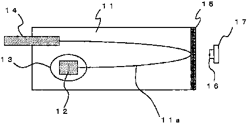
Fig. 1 shows an example of the structure of the latter optical
module. A branching waveguide is formed by a PLC. An optical fiber
14 is mounted, without being adjusted, on a PLC platform 11 by using a
V-groove. By this method, the optical fiber core and the waveguide lla
can be positioned at a micrometer level. Further, a semiconductor laser
12 and the optical fiber 14 can be coupled to the waveguide at a sub-
micrometer level, without the need of optical axis alignment, in such a
way that a mark pattern formed on the semiconductor laser 12 and a
mark pattern formed on the PLC platform 11 are matched with each
other by using infrared transmitted light.
In the optical module configured in this way, all the work of optical
axis alignment can be automated. This greatly contributes to reducing
the production cost of the optical module.
The optical module is configured such that an optical filter 15 is
arranged at a returning portion of the waveguide 1la, and that only light
CA 02636094 2008-06-25
3
of a specific wavelength is returned at the returning portion and light of
the other wavelengths is received by a PD 16 supported by a PD carrier
17.
As a device in which the passive alignment is used, there is a
wavelength tunable laser as shown in Fig. 2. This device is regarded as
a key device of the WDM transmission system and is energetically
studied in many research institutes. In the structure shown in Fig. 2,
three stages of ring resonators 24 are connected in series on a PLC
platform 21, and the waveguide is configured to be turned back by a
waveguide mirror 25.
A wavelength tunable operation is realized by performing phase
control in such a way that the refractive index is locally changed by
energizing a heater formed in the each ring resonator. One of the ring
resonators is adjusted to match a predetermined period (for example, a
period of ITU grid), so that a highly precise wavelength locking operation
is realized. An SOA (Semiconductor Optical Amplifier) 22 with phase
control, which is a type of the semiconductor optical element, is mounted
on the PLC platform 21 with high precision by the passive alignment.
As advantages of this structure, there are listed highly reliable
operation based on a structure with no movable portion, production cost
reduction based on a simple structure realized by integrating functions
as a wavelength tunable laser into one chip, and the like.
Usually, when a semiconductor optical element is mounted by the
passive alignment, Fresnel reflection is caused at a connection position
because of a difference in the refractive index between the waveguide
and the semiconductor optical element. In order to prevent the
reflection, there is used a refractive index matching gel with a refractive
index close to the refractive index of the waveguide of the PLC platform.
In the example shown in Fig. 2, even when a non-reflection coating is not
applied to the waveguide, it is possible to realize a stable operation with
CA 02636094 2008-06-25
4
little ripple in such a way that the non-reflection coating is not applied to
air but is applied to the refractive index matching gel 23 to thereby
prevent the reflection.
In Japanese Patent Laid Open Publication No. 2001-272582, there
is disclosed an invention in which a structure configured to make the end
of an adhesive layer recede to the inside from a light emitting surface is
adopted, and in which it is thereby prevented that the end of the
adhesive layer is extended to be raised to the emitting surface side and
projects in the optical path so as to shield the emitted light.
SUMMARY
The viscosity of the refractive index matching gel is generally low.
Thus, even when the refractive index matching gel is applied to only the
vicinity of the connection point between the waveguide and the SOA with
phase control, the gel is spread over a wide area. Therefore, in the case
where the refractive index matching gel is used, even when the end of
the coating area is set to the inside of the light emitting surface as in the
invention disclosed in Japanese Patent Laid Open Publication No. 2001-
272582, a part of the gel may be turned to reach the light emitting
surface, so as to thereby prevent the light emission. That is, a part of
gels may also be turned to reach the light emitting section of the SOA
with phase control. In this case, there is a possibility that the front
surface reflectance is made lower than a design value, or that the
efficiency of coupling with the optical fiber is lowered by deformation of
the light emitting surface.
In this way, the turning of the refractive index matching gel causes
a characteristic change and causes to lower the yield. In the case where
light is directly taken from the semiconductor optical element mounted
by the passive alignment as in the above described wavelength tunable
laser, it is important in particular to avoid the turning of the refractive
CA 02636094 2011-11-04
66446-734
index matching gel.
Some embodiments of the present invention have been made in view of
the above described problem. An exemplary object of some embodiments of the
present invention is to provide a mounting structure of a semiconductor
optical
5 element, in which structure the turning of the refractive index matching gel
is
prevented.
To this end, according to an aspect of the present invention, there is
provided a mounting structure of a semiconductor optical element, in which
structure
signal light emitted from one end of the semiconductor optical element mounted
to a
platform with an optical waveguide formed therein is made incident on the
optical
waveguide and is then again made incident on the semiconductor optical element
to
be emitted from the other end of the semiconductor optical element, wherein
the
semiconductor optical element is mounted to the platform in a state where the
other
end is projected from the platform, and wherein a refractive index matching
gel is
arranged between the one end of the semiconductor optical element and the
optical
waveguide.
According to one aspect of the present invention, there is provided a
semiconductor optical device comprising: a platform having a cross-section in
which
the platform is missing an exterior corner, the platform having an upper
horizontal
surface, a lower horizontal surface, and a middle horizontal surface between
the
upper and the lower horizontal surfaces, the platform having a left vertical
surface, a
right vertical surface, and a middle vertical surface between the left and the
right
vertical surfaces, the middle horizontal surface meeting the middle vertical
surface to
define an interior corner corresponding to the exterior corner missing in the
platform;
a mounting structure on the middle horizontal surface of the platform; an
emitting
semiconductor optical element attached to the mounting structure, the optical
element attached to the mounting structure in such a way that a left side of
the optical
CA 02636094 2011-11-04
66446-734
5a
element protrudes from the left vertical surface of the platform, an upper
side of the
optical element protrudes from the upper horizontal surface of the platform, a
first gap
is defined between a bottom side of the optical element and the middle
horizontal
surface of the platform, and a second gap is defined between a right side of
the
optical element and the middle vertical surface of the platform; and, a
refractive index
matching gel disposed at least within the first and the second gaps in such a
way that
at least the left side of the optical element remains at least substantially
uncovered by
the gel.
BRIEF DESCRIPTION OF THE DRAWINGS
Fig. 1 is a view showing a configuration of a common optical module;
Fig. 2 is a view showing a configuration of a wavelength tunable laser in
which ring resonance circuits are used;
Fig. 3 is a view showing a configuration of a semiconductor laser
according to a first exemplary embodiment in which the present invention is
preferably implemented;
Fig. 4 is a view showing a configuration of the semiconductor laser
according to the first exemplary embodiment; and
Fig. 5 is a view showing a configuration of a semiconductor laser
according to a second exemplary embodiment in which the present
CA 02636094 2008-06-25
6
invention is preferably implemented.
EXEMPLARY EMBODIMENT
[First Exemplary Embodiment]
There will be described a first exemplary embodiment in which the
present invention is preferably implemented.
Fig. 3 and Fig. 4 show a mounting structure of a semiconductor
optical element according to the present embodiment. An SOA 2 with
phase control is mounted on a PLC platform 1 by the passive alignment.
The passive alignment technique is a technique in which the positioning
is performed by using a mark pattern formed on the PLC substrate
surface and a mark pattern of an LD chip, and which eliminates the need
of optical axis alignment previously performed in manufacturing an
optical module and greatly improves the cost and the lead time for
producing the module.
In order to match the height of a waveguide 1la formed in the PLC
platform 1 with the height of a waveguide 2a formed in the SOA 2 with
phase control, pedestals 6 are arranged between the SOA 2 with phase
control and the PLC platform 1.
In the waveguide la coupled to the SOA 2 with phase control, three
stages of ring resonators 4 are formed. Further, the waveguide la is
configured to be turned back by a waveguide mirror 5, so that a
wavelength tunable operation is performed.
The end surface of the SOA 2 with phase control mounted by the
passive alignment is projected from the end surface of the PLC platform
1. With this configuration, even when a refractive index matching gel 3
with low viscosity is used, it is possible to prevent the refractive index
matching gel 3 from being turned to reach the light emitting end surface,
and thereby possible to prevent change in the oscillation characteristics
and deterioration in the coupling characteristics with the fiber.
CA 02636094 2008-06-25
7
With the configuration in which the end surface of the light taking-
out element (SOA 2 with phase control) is projected from the PLC
platform 1 in this way, it is possible to prevent the refractive index
matching gel 3 from being turned to reach the end surface of the element.
Thereby, it is possible to stabilize the oscillation characteristics and to
realize excellent coupling characteristics with the fiber with high yield.
[Second Exemplary Embodiment]
There will be described a second exemplary embodiment in which
present invention is preferably implemented.
Fig. 5 shows a configuration of a modulator integrated wavelength
tunable laser in the case where a modulator 7 is mounted as another
chip by the passive alignment in addition to the SOA 2 with phase
control. The configuration of the second exemplary embodiment is
almost the same as that of the first exemplary embodiment, but is
different in that the modulator 7 is further provided.
In this configuration, the oscillation characteristics can be more
stabilized as the reflectance of the emitting end of the modulator 7 is
reduced. For this reason, when the refractive index matching gel 3 is
brought into contact with the emitting end surface of the modulator 7,
the reflectance of the emitting end of the modulator is increased, so that
the oscillating operation of the wavelength tunable laser is made
unstable. In addition, the coupling characteristics with the fiber may be
deteriorated by the deformation of the emitting end surface.
In order to prevent such faults, it is configured such that the end
surface of the light taking-out modulator 7 is projected from the PLC
platform 1. This prevents the refractive index matching gel 3 from
being brought into contact with the emitting end surface of the
modulator 7, so that the stable operation and the excellent coupling
characteristics with the fiber can be realized.
In this way, with the configuration in which the end surface of the
CA 02636094 2008-06-25
8
light taking-out element (modulator 7) is projected from the PLC
platform 1, it is possible to prevent the refractive index matching gel 3
from being turned to reach the end surface of the light taking-out
element. Thereby, it is possible to stabilize the oscillation
characteristics and to realize excellent coupling characteristics with the
fiber with high yield.
Note that the above described embodiments are examples in which
the present invention is preferably implemented, but the present
invention is not limited to these.
For example, the each embodiment as described above is configured
such that the wavelength tunable operation is performed by using the
three stages of ring resonators, but the number of stages of ring
resonators can be arbitrarily set. Further, as long as the wavelength
tunable operation can be performed, the ring resonator need not be
necessarily used.
Further, the each embodiment as described above is configured
such that the SOA with phase control is used as an example of a
semiconductor optical element. However, it is needless to say that the
present invention can be applied to all semiconductor optical elements
including a semiconductor laser.
In this way, various modifications are possible within the scope and
spirit of the present invention.