Note : Les descriptions sont présentées dans la langue officielle dans laquelle elles ont été soumises.
CA 02637038 2008-07-11
WO 2007/089341 PCT/US2006/048020
APPARATUS AND METHODS FOR PACKAGING INTEGRATED CIRCUIT CHIPS
WITH ANTENNAS FORMED FROM PACKAGE LEAD WIRES
Technical Field of the Invention
The present invention generally relates to apparatus and methods for
integrally
packaging semiconductor IC (integrated circuit) chips with antenna structures
that are formed
using chip package lead wires, to thereby provide highly-integrated
radio/wireless
communications systems for millimeter wave applications.
Background
Technological innovations in wireless systems and devices have lead to
widespread
development of wireless network applications for wireless PAN (personal area
network),
wireless LAN (local area network), wireless WAN (wide area network), cellular
networks,
and other types of wireless communication systems. To enable wireless
communication
between devices in a wireless network, the devices must be equipped with
receivers,
transmitters, or traiisceivers, as well as antennas that can efficiently
radiate/receive signals.
transmitted to/from other devices in the network.
Conventional radio communication systems are typically constructed using
discrete
components that are individually encapsulated and/or mounted with low
integration levels on
printed circuit boards; packages or substrates. For example, FIG. 1
schematically illustrates a
conventional radio communication system (10). The system (10) comprises a
leaded chip
package (11) =with an,integrated circuit chip (12) and protruding package
leads (13). The
package=leads-(13) are connected to interconnect structures (14) that are
formed-on. a PCB
(printed circuit board) or printed wiring board, for example. The interconnect
structures (14) -
provide electrical connections to a transmitter or receiver antenna (15) (such
as a printed
antenna structure formed on the board level). The electrical interconnects
(14) are typically
built using expensive and bulky wave guides and/or package-level or board-
level micro strip
str.uctures.
There is an increasing market dernand,, however, for more compact radio
communication systems with integrated transmitter/receiver/transceiver and
antenna systems,
which provide high-performance, high data transmission rate, high-volume, low-
power
consumption, low cost, and low weight solutions. Indeed, current communication
systems
require high performance antenna systems that provide, e.g., wide bandwidth,
high-gain, and
high-efficiency operating characteristics. As the operating frequency
increases, the
1
CA 02637038 2008-07-11
WO 2007/089341 PCT/US2006/048020
manufacture and assembly of conventional waveguide front-ends become more
difficult. In
this regard, innovations in semiconductor fabrication and packaging
technologies, coupled
with requirements for higher operating frequencies, have made it practically
feasible for
integrating antennas with RF integrated circuits to provide highly integrated
radio
i communication systems.
Summary of the Invention
In general, exemplary embodiments of the invention include apparatus and
methods
for integrally packaging semiconductor IC (integrated circuit) chips with
antennas that are
formed using chip package leads as radiating elements, to thereby provide
highly-integrated
radio/wireless communications systems for millimeter wave applications.
In one exeinplary embodiment, an electronic apparatus includes an IC
(integrated
circuit) chip and an antenna system, wherein the IC chip and antenna system
are -integrally
packaged together in a leaded chip-scale package. The antenna system includes
an antenna
having a radiating element that is formed from a package lead wire. The
radiating element
may be a straight lead wire, a lead wire having at least one bend or an
inverted gull wing lead
wire, for example. In another exemplary embodiment, the antenna includes a
tuning element
formed from a package lead wire disposed in proximity to the radiating
element.
In yet another exemplary embodiment, the apparatus includes an integrated
antenna feed
network having an on-chip feed structure formed on- an active surface of the
IC chip and a
wire bond connecting the on-chip feed structure to one end of the radiating
element. The on-
chip feed structure may be a CPW (coplanar waveguide which includes a center
conductor
wire bond connected to the radiating element of the antenna, and first and
second ground
elements disposed bn, and spaced apart from, opposite edges of the center
conductor. The
antenna system my have a tuning element formed from a lead wire disposed in
proximity to
the radiating element, wherein the tuning element is wire bonded to one of the
first and
second ground elements of the CPW.
In another exemplary embodiment, the on-chip feed structure includes a
balanced
differential feed line including first and second coplanar feed lines, wherein
the radiating
element of the antenna is wire bonded to the first feed line. The antenna may
further
) comprise a second radiating elernerit wire bonded to the second feed line,
wherein the =first
and second radiating element together form a balanced antenna structure such
as a dipole. In
another embodiment,. the antenna may include a tuning element formed from a
lead wire
2
CA 02637038 2008-07-11
WO 2007/089341 PCT/US2006/048020
disposed in proximity to the radiating element, wherein the tuning element is
wire bonded to
the second feed line.
In another exemplary embodiment of the invention, a wireless communication
apparatus is provided; which includes a printed circuit board, and a chip
package mounted to
the printed circuit board. The chip package comprises an IC (integrated
circuit) chip and
antenna system integrally packaged together in a leaded chip-scale package,
wherein the
antenna system comprises an antenna having a radiating element that is formed
from a
package lead wire. In another embodiment, the printed circuit board includes a
metallic
ground structure that functions as an antenna ground element, a radiation
reflector, or both.
- In various embodiments of the invention, the radiating element may be a
straight,
open-ended lead wire that extends substantially parallel to, and spaced apart
from, a metallic
ground element, or the radiating element may be a close-ended lead wire having
a bent
portion connected-to the metallic ground element, or the radiating element may
be an open-
ended inverted gull wing lead wire disposed over the metallic ground element.
In other
exemplary embodiments of the invention, the antenna may include one or more
close-ended
and/or open-ended tuning elements disposed in proximity to one or more
radiating elements.
These and other exemplary embodiments, aspects, objects, features and
advantages of
the present invention will be described or become apparent from the following
detailed
description of exerimplary embodiments, which is to be read in connection with
the
accompanying drawings. Brief Description of the Drawings
FIG. I schematically illustrates a conventional radio communication system.
FIG. 2 is a high-level schematic illustration of an apparatus for integrally
packaging an
IC chip and antenna structure formed from one or more package lead wires,
according to an
i exemplary embodiment of the invention.
FIGs. 3A and 3B schematically illustrate an electronic package apparatus
according to
an exemplary embodiment of the invention, for integrally packaging an IC chip
and antenna
structure formed Trom one or more package lead wires.
FIGs. 4A and 4B depict exemplary layout and structural dimensions for the
exemplary
) package structure of FIGs. 3A and 3B to form an integrated radio
communication system
operating at a frequency of about 60GHz.
3
CA 02637038 2008-07-11
WO 2007/089341 PCT/US2006/048020
FIGs. 5A and 5B schematically illustrate a grounded coplanar wave guide
structure
according to an exemplary embodiment of the invention.
FIG. 6A schematically illustrates an integrated antenna system according to an
exemplary embodiment of the invention.
FIG. 6B graphically illustrates a simulated return loss of the antenna
structure of FIG.
6A.
FIG. 6C graphically illustrates a simulated radiating efficiency of the
exemplary
antenna system of FIG. 6A.
FIG. 7A schematically illustrates an integrated antenna system according to an
exemplary embodiment of the invention.
FIG. 7B graphically illustrates a simulated return loss of the antenna
structure of FIG.
7A.
FIG: 8A schematically illustrates an integrated antenna system according, to
an
exemplary embodiment of the invention.
FIG. 8B graphically illustrates a simulated return loss of the antenna
structure of FIG.
8A.
FIG. 9A schematically illustrates an integrated antenna system according to an
exemplary embodiment of the invention.
FIG. 9B graphically illustrates a simulated return loss of the antenna
structure of FIG. 9A. FIGs..1 UA and l OB schematically illustrate an
integrated antenna system according to
an exemplary. embodiment of the invention. FIG. l OC graphically illustrates a
simulated return loss of the antenna structure of
FIGs. 10A-B. .
Detailed Description of Exemplary Embodiments
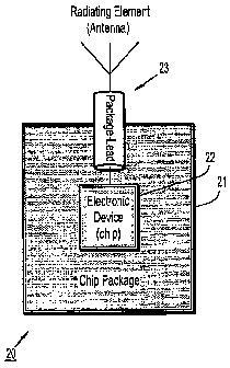
FIG: 2 is. a high-level schematic illustration of an apparatus for integrally
packaging
IC chips and antennas according to an exemplary embodiment of the invention.
In particular,
FIG. 2 depicts an apparatus (20) comprising a chip scale package structure
(21) comprising an
IC chip (22) and antenna (23) that is formed from one or more package lead
wires of a lead
frame of the package (21). The IC chip (22) may comprise a radio communication
system-
on-chip including an integrated receiver, transmitter or transceiver system,
which operates at
millimeter wave frequencies (e.g., 20 GHz and greater). The IC chip (22) may
comprise other
4
CA 02637038 2008-07-11
WO 2007/089341 PCT/US2006/048020
integrated RF active or passive devices/circuits such as antenna feeds,
transmission lines, low
noise amplifiers, filters, etc.
In accordance with exemplary embodiments of the invention, various types of
leaded
package technologies can be used to form package lead frame structures having
one or more
package lead wires that are sized, shaped and/or arranged to form an antenna
structure. In
general, leaded chip packages are typically named based on the shape of the
lead wires, e.g.,
gull-wing leads, S-leads, C-leads, or straight I-leads. During a chip
packaging process, the
package lead wires are typically shaped after a package molding process. The
package lead
wires are initially formed as straight wires that are mechanically supported
with a metal ring
attached to the component body, which protects the lead wires from damage
during handling.
Subsequently, the ring is excised using a suitable tool and the package leads
are shaped using
a universal trim and form device.
It is to be appreciated that during a lead forming process, one or more lead=
wires can
be sized, shaped and arranged to form an antenna structure having desired
antenna
characteristics such ag resonant operating frequency, radiation efficiency,
gain,- operation
bandwidth, etc. The lead wire(s) can be designed with a given length such that
most of the
lead wire(s) protrudes from, and is not covered by, lossy insulation material
that is used to
form the package fnold (or encapsulation). Indeed, lead wires can be shaped
and sized to as
radiating elements which protrude from the package structure such that most of
the antenna
area is surrounded by air.
In other exemplary embodiments described in further detail, antenna.structures
with.
lead wire antenna elements can be designed in conjunction with board-level
ground planes
and/or ground connections, if necessary. In particular, depending on the
application, lead
wire antenna elements can be terminated on the board-level with an open or
short circuit to
provide required boundary conditions. A board-level ground plane can be used
as a ground
termination for an antenna lead wire elements, can operate as an antenna
ground plane for
monopole radiators, and can operate as a reflecting surface to direct
radiation in a given
direction.
In other exemplary embodiments of the invention described in detail below,
antenna
structures can,be formed using one or more grounded or open-ended lead wire
elements
(tuning elements) that are disposed =in proximity to a radiating lead wire
element for purposes.
of tuning the antenna to achieve desired antenna properties. The lead wire
tuning -elements
CA 02637038 2008-07-11
WO 2007/089341 PCT/US2006/048020
can be sized, shaped and arranged for purposes of controlling antenna
impedance, increasing
antenna bandwidth, control antenna radiation patterns, etc.
FIGs. 3A and 3B schematically illustrate an electronic package apparatus (30)
according to an exemplary embodiment of the invention, for integrally
packaging an IC chip
and antenna structure formed from one or more package lead wires. FIG. 3A is a
top plan
view of the apparatus (30) and FIG. 3B is a side-view of the apparatus (30)
along line 3B-3B
in FIG. 3A. The apparatus (30) comprises a package mold (31) (or package
encapsulation), a
carrier substrate (32) (or package frame structure), an IC chip (33), a
plurality of package lead
wires (34), (35), (36), and wire bond connections (37, (38). The electronic
package (30) is
depicted as being mounted to a PCB (printed circuit board) (39) having a
metallic ground
plane (39a) on a surface thereof. The metallic ground plane (39a) can serve as
an antenna
ground plane and/or radiation reflector.
The carrier substrate (32) and lead wires (34), (35) and (36) are part of a
metallic lead
frame structure that is formed using known techniques (e.g., etching,
stamping). The die
paddle (32) serves to mechanically support the IC chip (33) during package
manufacture. The
IC chip (33) is backside mounted to the substrate (32) during a die mounting
process using
known techniques. The IC chip (33) (or die) may comprise an integrated radio
communications system (e.g., receiver, transmitter, transceiver, etc.). The
lead wires (34),
(35) and (36) are connected to appropriate bond pads on the active surface of
the chip (33) by
wire bonds (37) and (38) during a wire bonding process. The lead wires (34)
provide I/O
connections and power supply connections between external wiring/pads on
the'PCB (39) and
BEOL (Back-end-of-line) pads/wiring on the active surface of the IC chip (33).
Further, in the exemplary embodiment of FIGs. 3A and 3B, the package lead wire
(36)
is formed to operate.as a radiating element of an antenna structure. The
package lead wire
(36) is shaped as an inverted gull-wing lead, although this is merely
exemplary and other lead
wire shapes are possible to form antenna radiating elements. In other
exemplary embodiments
of the inventibn, a-plurality of lead wires can be formed as radiating
elements to. construct'
various types of antenna. structures including, for example, antenna arrays or
multi-band
antennas,=etc.
- As noted above, antenna structures according to exemplary embodiments of the
invention can bc formed using one or more grounded or open ended lead wire
elements that
are disposed in proximity to a radiating lead wire element for purposes of
tuning the antenna
~ 6 ,
CA 02637038 2008-07-11
WO 2007/089341 PCT/US2006/048020
to achieve desired antenna properties. For example, in the exemplary
embodiment of FIGs.
3A/3B, the lead wires (35) may be used as antenna tuning elements disposed on
either side of
the radiating element (36) and connected to the ground plane (39a) of the PCB
(39). The lead
wire elements (35) are sized, shaped and arranged for purposes of controlling
antenna
impedance, increasing antenna bandwidth, control antenna radiation patterns,
etc. In the
exemplary embodiment of FIGs. 3A/3B, the antenna structure with radiating
element (36) and
tuning elements (35) is formed in conjunction with the board-level ground
plane (39a) formed
on the PCB (39), where the radiating element (36) is open-ended with respect
to the ground
plane (39a) and the tuning elements (35) having terminating ends that are
short-circuited to
the ground plane (39a) (or ground pads/contacts). Again, depending on the
application, the
lead wires that form an antenna structure can be terminated on the board-level
with an open
or short circuit to provide required boundary conditions. Antenna structures
according to
other exemplary embodiments of the invention which utilize board-level ground
structures
will be discussed below with reference to the exemplary embodiment depicted in
FIGs. 6A,
7A, 8A, 9A and 10A, for example.
According to 'further embodiments of the invention, integrated chip-to-antenna
connections are realized in an impedance-controlled fashion by feed networks
that are
constructed with bond wires and on-chip feed structures to provide a desired
anterina input
impedance. For example, antenna feed networks according to exemplary
embodiments of the
invention include ori-chip feed structures, such as CPW (coplanar wave guide);
differential
feed lines; etc, which are formed as part of BEOL metallization of an IC chip,
and bond wires
to 'connect the on-chip feed structures to lead wire antenna elements.
Integrated antenna
systems'having on chip feed structures that are formed from on-chip feed
structures and bond.
wires according to exemplary embodiments of the invention will be discussed
below with
reference'to the exemplary embodiments depicted in FIGs. 6A, 7A, 8A, 9A and
10A, for
example. . .
FIGs. 4A and 4B illustrate dimensions of the electronic package apparatus (30)
depicted in FIGs. 3A and 3B, for constructing an integrated radio
communications system that
operates at a fundamental frequency of about 60GHz. In the exemplary
embodiment, the
package mold (31) is depicted as having a thickness of 1 mm, a length of 5 mm,
and a
package offset of 100 microns. The package mold (31) can be formed of a
material (plastic,
epoxy) preferably having a relatively low dielectric constant and relatively
low dielectric loss.
7
CA 02637038 2008-07-11
WO 2007/089341 PCT/US2006/048020
The lead wire elements (34), (35) and (36) are formed of copper (or other
suitable metallic
material) and have a width of 300 microns, while the width of the bond wire
(37) is 50
microns. The ground plane (39a) formed on the surface of the PCB (39) is
disposed below
the antenna lead wire elements (35) and (36). The overall length of the lead
wire elements
(35) and (36) is 2.2 mm and are separated by a pitch of 500 microns. The
length of an upper
bent portion (36a) of the element (36), which has an exemplary length of 600
microns, affects
the resonant frequency. The 1.2 mm spacing between the upper bent portion
(36a) and the
ground plane (39a) affects the bandwidth of the antenna. The antenna lead wire
elements (35),
(36) are connected to an antenna feed network formed by bond wires (37) and an
on-chip feed
structure (e.g., CPW) on the active surface of the chip (33).
FIGs. 5A and 5B schematically illustrate an antenna feed structure according
to an
exemplary erimbodiment of the invention. In particular, FIGs. 5A and 5B
illustrate coplanar
waveguide (CPW) structure for implementing an unbalanced feed network for
feeding
antenna structures formed with package lead wires, according to an exemplary
embodiment of
the invention. FIG. 5A is a plan view of a CPW feed (50) structure which
comprises a center
conductor (50a) separated from a pair of ground elements (50b, 50c). The
elements (50a, 50b
and 50c) of the CPW (50) are coplanar (formed on same plane). The CPW (50) can
be formed
on-chip as part of an upper metallization layer of a BEOL interconnect
structure. FIG. 5B
schematically'illustrates the CPW feed structure embedded in a center plane
region (50') 6f a
dielectric medium (51). The dielectric medium (51) is disposed over a ground
plane (59a) of
a PCB (59).. ,
Computer simulations were performed for a CPW feed structure having the
exemplary
structural diniensions shown in FIGs 5A and 5B to provide a 75 ohm CPW. In the
exemplary
embodiment of FIG. 5A, the ceinter conductor (50a) was defined having a length
of 500
microns and width of 100 microns. The ground elements (50b) and (50c) were
defined
having similar dimensions length x=width of 500 microns x 500 microns. The
center
conductor (50a) was spaced apart from each ground element (50b) and (50c) by
50 microns.
In FIG. 513; the dielectric medium (51) was defined having a thickness of lmm
and spaced
apart from the grourid plane (59a) by 100 microns. The CPW feed structure (50)
was spaced '
apart from the ground plane (59a) by a distance of 600 microns. The dielectric
medium (51)
was defined as being.formed of a material with a dielectric constant of 2.7
and loss tangent of
0.04. ~
8
CA 02637038 2008-07-11
WO 2007/089341 PCT/US2006/048020
It is to be appreciated that a CPW structure, such as depicted in FIG. 5A,
together with
wire bonds, can be used to form antenna feed networks for unbalanced feeding
of antennas
that are formed from lead wire elements. For instance, various antenna systems
designed
with open-ended and grounded lead wire antenna elements fed by CPW feed
networks, will
be discussed with reference to the exemplary embodiments of FIGs. 6A, 7A, 8A
and 9A. For
purposes of determining electrical performance, properties and characteristics
of the
exemplary CPW fed antenna structures of FIGs. 6A, 7A, 8A and 9A, computer
simulations
were performed based on exemplary dimensions of the antenna elements and feed
structures
depicted in FIGs. 6A, 7A, 8A and 9A for a fundamental operating frequency of
about 60GHz.
The results of the computer simulations will be discussed below with reference
to FIGs. 6B,
6C, 7B, 8B and 9B. For each of the computer simulations, the antenna CPW feed
structures
in FIGs. 6A, 7A, 8A. and 9A were assumed to be embedded in a dielectric medium
and spaced
from a ground plane as per the exemplary dimensions and dielectric
characteristics as
discussed with reference to FIG. 5B.
FIG. 6A schematically illustrates an integrated antenna system according to an
exemplary embodiment of the invention. In particular, FIG. 6A illustrates an
antenna feed
network (60) comprising a CPW structure (61) and wire bond (62), which feeds
an antenna
structure comprising a-radiating element (65). In the exemplary embodiment,
the radiating
element (65) is a straight, open-ended package lead wire that is disposed
parallel. to and
separated from a ground plane (64). The CPW structure (61) comprises a center
conductor
(61 a) and adjacent *ground elements (61b) and (61c). The wire bond (62)
provides an
electrical connection between the center conductor (61a) of the CPW (60) and
one end (fed
end) of the lead wire radiating element (65). The antenna feed network (60)
and fed end of
the radiating element'(65) are embedded within a dielectric medium (63).
FIG. 6A illustfates exemplary layout and structural dimensions that were
defined for ~
computer simulation of the antenna system of FIG. 6A for an operating
frequency of about 60
GHz. In FIG.= 6A, the antenna element (65) was defined having a length of 2050
microns. In
the exemplary embodiment, the length LI, which includes the wire bond (62) and
a portion of
element (65) (embedded in the dielectric (63)) is selected to be about one-
quarter wavelength
- of the operating f~equency, and the length L2 is selected to be about one-
half wavelength of
the operating frequeney. The elements of the CPW structure (61) were defined
to have the.
same planar dimensions as discussed with reference to FIG. 5A, with the CPW
structure (61)
9
CA 02637038 2008-07-11
WO 2007/089341 PCT/US2006/048020
being disposed from side of the dielectric medium (63) by 1500 microns. The
dielectric
medium (63) was defined having that thickness and spacing dimensions as
depicted in FIG_
5B.
0
FIGs. 6B and 6C illustrate simulation results for the exemplary antenna system
of
FIG. 6A. In particular, FIG. 6B graphically illustrates a simulated return
loss of the antenna
structure normalized to 31 Ohms and, in particular, the simulated return loss
(S 11) in dB for a
frequency range of 50 - 70 GHz. The simulation results in FIG. 6B illustrate a
bandwidth of
at least 4 GHz, wherein bandwidth is defined based on the frequency range for
which S>> was
measured to be about -10dB or better. FIG. 6C graphically illustrates a
simulated radiating
efficiency of the exemplary antenna system of FIG. 6A over the frequency range
of 50 - 70
GHz. The results of the simulation illustrate a radiation efficiency of 80% or
better over the
frequency range of 59-64 GHz.
FIG. 7A schematically illustrates an integrated antenna system according to
another
exemplary einbodiment of the invention. In particular, FIG. 7A illustrates an
antenna feed
network (70) comprising a CPW structure (71) and wire bond (72), which feeds
an antenna '
comprising radiating element (75). In the exemplary embodiment, the radiating
element (75)
is a grounded lead wire having a straight portion of length L disposed
parallel to and
separated from a ground plane (74), and an unfed (terminating) end that is
bent toward and
connected to the ground.plane (74). The CPW structure (71) comprises a center
conductor.
(71 a) and adj acent ground elements (71 b) and (71 c): The wire bond (72)
provides an
electrical connection between the center conductor (71a) of the CPW (70) and
one end of the
lead wire radiating element (75). The antenna feed network (70) and fed end
portion of the
radiating element (75) are embedded within a dielectric medium (73). Unlike
the antenna
structure in FIG. 6A, 'where the radiation pattern has only one horizontal
polarization, the .
antenna in FIG. 7A has both horizontal and vertical polarizations.
FIG. 7A illustrates exemplary layout and structure dimensions that were
defined for
computer simulation of the antenna system of FIG. 7A for an operating
frequency of about 60
GHz. In FIG. 7A, the antenna element (75) was defined having a length L of
3050 microns. In
the exemplary embodiment, the length L1, which includes the wire bond (72) and
a portion of
- element (75) (embedded in the dielectric (73)) is selected to be about one-
quarter wavelength
of the operating frequency, and the length L2 is selected to be about three-
quarters
wavelength of the. operating frequency. The CPW structure (71) was defined
being disposed '
CA 02637038 2008-07-11
WO 2007/089341 PCT/US2006/048020
from side of the dielectric structure (73) by 1500 microns, but having a
narrower dimension
of 600 microns (as compared to the 1200 microns of the CPW structure (60) of
FIG. 6A). The
dielectric medium (73) was defined having the exemplary thickness and spacing
dimensions
as depicted in FIG. 5B.
FIG. 7B illustrates the simulation results for the exemplary antenna system of
FIG.
7A. In particular, FIG. 7B graphically illustrates a simulated return loss of
the antenna
structure normalized to 37 Ohms and, in particular, the simulated return loss
(S11) in dB for a
frequency range of=50 - 70 GHz. The simulation results in FIG. 7B illustrate a
bandwidth of
at least 2.5 GHz, wherein bandwidth is defined based on the frequency range
for which SI~
was measured to be about -10dB or better.
FIG. 8A schematically illustrates an integrated antenna system according to
another =
exemplary embodiment of the invention. In particular, FIG. 8A illustrates an
antenna feed
network (80)-comprising a CPW structure (81) and wire bonds (82) and (87),
which feeds an
antenna =structure eomprising a radiating element (85) and a tuning element
(86) formed from
package leads.. The CPW structure (81) comprises a center conductor (81 a) and
adjacent
ground elements .(81 b) and (81c). The wire bond (82) provides an electrical
connection
between the center conductor (81a) of the CPW (80) and one end of the
radiating element
(85). The wire bond (87) provides an electrical connection between the ground
element (81b)
of the=CPW (80) and the tuning element (86). The antenna feed network (80) and
fed ends of
the radiating and tpning elements (85) and (86) are embedded within a
dielectric medium =
(83).
In the exemplary embodiment of FIG. 8A, the radiating element (85) is an open-
ended, straight package lead wire that is disposed parallel to and separated
from a ground
plane (84). Moreover, the tuning element (86) is an open-ended straight
package lead wire
that extends parallel to, and spaced apart from, both the ground plane (84)
and the antenna
radiating element (85). As compared to the antenna system of FIG. 6A, the
antenna system of
FIG. 8A includes the tuning element (86) disposed in proximity to the
radiating =element (85).
as a means'to adjust the antenna resonate frequency and impedance due to the
EM coupling
between the'anteiina elements (85) and (86).
FIG. 8A illustrates exemplary layout and structure dimensions that were
defined for '=
computer simulation of the antenna system of FIG. 8A for an operating
frequency of about 60
GHz. In FIG.= 8A, the antenna radiating element (85) was defined having a
length of 2050
~ 11
CA 02637038 2008-07-11
WO 2007/089341 PCT/US2006/048020
microns and the antenna tuning element (86) was defined having a length of
1500 microns.
Moreover, the dimensions of the ground elements (81b) and (81c) of the CPW
structure (81)
were dissimilar, with the ground element (81b) connected to the tuning antenna
element (86)
being wider than the ground element (81 c). The dielectric medium (83) was
defined having
the exemplary thickness and spacing dimensions as depicted in FIG. 5B.
FIG. 8B illustrates the simulation results for the exemplary antenna system of
FIG.
8A. In particular, FIG. 8B graphically illustrates a simulated return loss of
the antenna
structure normalized to 31 Ohms and, in particular, the simulated return loss
(S11) in dB for a
frequency range of 50 - 70 GHz. The simulation results in FIG. 8B illustrate a
bandwidth of
at least 4GHz, wherein bandwidth is defined based on the frequency range for
which S iI was
measured to be about -10dB or better. Comparing the simulation results
depicted in FIGs. 6B
and 8B, it is shown. that the additional lead wire tuning element (86)
proximately disposed to
the radiating element (85) results in a shift in the antenna resonate
frequency and impedance.
FIG. 9A schematically illustrates an integrated antenna system according to
another
exemplary embodiment of the invention. In particular, FIG. 9A illustrates an
antenna feed
network (90) comprising a CPW structure (91) and wire bonds (92), (97) and
(99), which
feeds ari antenna structure comprising a radiating element (95) and tuning
elements (96) and
(98) formed by package lead wires. The CPW structure (91) comprises a center
conductor=
(91a) and adjaceiit ground elements (91b) and (91c). The wire bond (92)
provides an
electrical connection between the center conductor (91a) of the CPW (91) and
one end of the
radiating element (95). The wire bond (97) provides an electrical connection
between the
ground element (91b) of the CPW (91) and the antenna tuning element (96). The
wire bond
(99) provides =an electrical connection between the ground element (91 c) of
the CPW (91) =and
the antenna tuning element (98). The antenna feed network (90) and fed ends of
the radiating.
and tuning elemepts (95), (96) and (98) are embedded within a dielectric
medium (93).
In the exemplary embodiment of FIG. 9A, the radiating element (95) is formed
from
an open-ended, straight lead wire that is disposed parallel to and separated
from a ground
plane (94). Moreover, the tunirig elements (96) and (98) are formed from open-
ended straight
lead wires that extend parallel to the ground plane (94) and on opposite sides
of the antenna
radiating element (95). As compared to the antenna system of FIG. 8A, the
antenn'a system of
FIG. 9A includes a,plurality of tuning elements (96) and (98) disposed in
proximity to, and on
opposite sides of, the radiating element (95) as a means to adjust the antenna
resonate
12 =
CA 02637038 2008-07-11
WO 2007/089341 PCT/US2006/048020
frequency and impedance due to the EM coupling between the antenna elements
(95) and (96)
and (98).
FIG. 9A illustrates exemplary layout and structure dimensions that were
defined for
computer simulation of the antenna system of FIG. 9A for an operating
frequency of about 60
i GHz. In FIG. 9A, the antenna element (95) was defined having a length of
2050 microns and
the antenna tuning elements (96) and (98) were defined having a length of 1500
microns.
Moreover, the dimensions of the ground elements (91b) and (91 c) of the CPW
structure (91)
were similarly defined. The dielectric medium (93) was defined having the
exemplary
thickness and spacing dimensions as depicted in FIG. 5B.
FIG. 9B illustrates the simulation results for the exemplary antenna system of
FIG.
9A. In par ticular, FIG. 9B graphically illustrates a simulated return loss of
the antenna
structure normalized to 31 Ohms and, in particular, the simulated return loss
(S11) in dB for a
frequency range of 50 - 70 GHz. The simulation results in FIG. 8B illustrate a
bandwidth of
at least 2.5GH4 wherein bandwidth is defined based on the frequency range for
which S>
was measured to be about -10dB or better. Comparing the simulation results
depicted in FIGs.
6B, 8B and 9B, it is shown that the additional lead wire element (99)
proximately disposed'to
the radiating element (92) results in a shift in the antenna resonate
frequency and impedance.
FIGs.= l0A and l OB schematically illustrate an integrated antenna system
according to
another exemplary embodiment of the invention. In particular, FIG. 10A
illustrates an.
antenna feed network (1000) comprising a balanced differential feed lines
(1001) and wire
bonds'(1002) and (1007), which feeds an antenna structure comprising a
radiating element
(1005) and a tuning element (1006) formed from package leads. The differential
feed
structure (1001)=comprises two coplanar feed lines (1001a) and (1001b). The
wire bond
(1002) provides an electrical connection between differential line (1001 a)
and one end of the
radiating element (1005). The wire bond (1007) provides an electrical
connection between
the differential line (1001b) and the tuning element (1006). The antenna feed
network (1000)
and fed ends of the.radiating and tuning elements (1005) and (1006) are
embedded within a
dielectric medium (1003).
FIG: l OB is a perspective view of the exemplary antenna system of FIG. l 0A.
In the
exemplary embodiment of FIG: IOB, the radiating element (1005) is an open-
ended, package
lead wire that is shaped as an inverted gull wing lead having a straight
portion (1005a), and
bent portions (1005b) and (1005c), Moreover, the tuning element (1006) is an
close-ended
13 .
CA 02637038 2008-07-11
WO 2007/089341 PCT/US2006/048020
package lead wire having a straight portion (1006a) which extends parallel to,
and spaced
apart from, both the ground plane (1004) and the portion (1005a) of the
radiating element
(1005). In addition, the tuning element (1006) has a bent portion (1006b)
which extends
down from the end of the straight portion (1006a) towards the ground plane
(1004) and
contacts the ground plane (1004).
FIGs. 10A and 10B illustrate exemplary layout and structure dimensions that
were
defined for computer simulation of the antenna system for an operating
frequency of about 60
GHz. In FIG. 10A, the antenna radiating element (1005) was defined having a
length (in the x
direction) of 1300+200+200 microns and the antenna tuning element (1006) was
defined
having a length (in the x direction) of 1300+200 microns. Moreover, the
balanced feed lines
(1001 a, 1001 b) are 'separated by a pitch of 150 microns (where the pitch can
be modified to
tune the feed line impedance). An exemplary offset distance was defined to.be
175 microns.
This offset distance can be varied to adjust a separation between (1005) and
(1006) to thereby
tweak the antenna performance. An exemplary length of 400.microns was defined
between
the wirebonds (10fJ2) and (1007) in the "x" direction between feedline (1001)
and lead wires
(1005, 1006) (which length can be varied to change the antenna resonant
frequency.) The
dielectric.medium (1003) was defined having the exemplary thickness and
spacing
dimensions as depicted in FIG. 5B.
FIG: l OC illustrates the simulation results for the exemplary antenna system
of FIGs.
10A and 10B: In particular, FIG. l OC graphically illustrates a simulated
return loss of the
differential fed antenna structure normalized to 150 Ohms and, in particular,
the simulated
return loss (S 11) in dB for a frequency range of 50 - 70 GHz. The simulation
results in FIG. -
l OC illustrate a bandwidth of at least 6 GHz, wherein bandwidth is defined
based on the
frequency range for which S11 was measured to be about -10dB or better.
Comparing the
simulation results depicted in FIGs. 6B, 7B, 8B, 9B and 10C, it is shown that
the differential -
fed antenna structure provides a relatively wider operating bandwidth mainly
due to the
relatively large separation between the radiating element (1005) and the
ground plane (1004).
In another exemplary embodiment of the invention, the antenna framework of
FIGs.
10A and l OB can be modified such that element (1006) is not grounded, but
rather the
elemeints (1005) and (1006) are formed into a balanced antenna structure such
as a dipole
antenna fed by the balanced differential line. For example, the leads (1005)
and (1006) can.
14
CA 02637038 2008-07-11
WO 2007/089341 PCT/US2006/048020
be bent away from each other in opposite directions in the y direction to form
a half-
wavelength dipole radiator.
The integrated antenna systems discussed above are merely exemplary
embodiments
to illustrate the use of package lead wires to form antenna structures. Based
on the teachings
herein, one of ordinary skill in the art can readily envision other
embodiments in which one or
more lead wires can be formed to operate as antenna radiating elements to form
antenna
structures including, for example, antenna arrays and multiband antenna
structures and
wherein one or more package lead wires are formed to operate as antenna tuning
elements to
control antenna impedance, to increase antenna bandwidth or control antenna
radiation
patterns. The exemplary antenna structures discussed above are meant to
illustrate the
flexibilities of the antenna design with lead wires, and should not be
construed as limiting the
scope of the claimed inventions. For instance, in the exemplary embodiments of
FIGs. 8A
and 9A, the tuining elements can be formed instead as radiating elements
having resonant
frequencies that enable multi-band operation. By way of specific example, in
FIG. 8A, the
elements (85) and (86) can be separate radiating elements having resonant
frequencies in
different frequency bands to provide dual-band operation, and the elements
(95), (96) and
(98) in FIG. 9A can be separate radiating elements having resonant frequencies
in different
frequeney bands to provide tri-band operation:
Those of ordinary skill in the art will readily appreciate the various
advantages
associated with antennas and integrated antenna packages according to
embodiments of the
invention. For instance, exemplary antenna designs which are integrally
fornied using
package lead wires using known techniques enables high-volume antenna
manufacturing
capability. Moreover, integrated IC packages according to exemplary
embodiments of the
invention enable antennas to be integrally packaged with IC chips such as
transceiver chips,
which provide compact designs with very low loss between the transceiver and
the=antenna.
Moreover, the use of integrated antenna/IC chip packages according to the
present invention
saves significant space, size, cost and weight, which is a premium for
virtually any
commercial or military application.
Although exemplary embodiments have been described herein with reference to
the
accompanying drawings for purposes of illustration, it is to be understood
that the present
invention is not limited to those precise embodiments, and that various other
changes and
CA 02637038 2008-07-11
WO 2007/089341 PCT/US2006/048020
modifications may be affected herein by one skilled in the art without
departing from the
scope of the invention.
16