Note : Les descriptions sont présentées dans la langue officielle dans laquelle elles ont été soumises.
CA 02637228 2008-07-15
WO 2007/117187
PCT/SE2006/050065
A METHOD AND APPARATUS FOR REDUCING FREQUENCY MEMORY EPI-ECTS IN RF POWER
AMPLIFIERS
TECHNICAL FIELD OF THE INVENTION
The present invention relates to power amplifying techniques in general and to
a method and
apparatuses for reducing frequency memory effects in (RE) power amplifiers in
particular.
DESCRIPTION OF RELATED ART
Power amplifiers are indispensable components in a communication system and
are known to
add more or less distortion to the signal they are designed to amplify,
especially in
multicarrier telecommunications systems (e.g. WCDMA) which are particularly
sensitive to
distortion. The reason for this is that power amplifiers have a non-linear
input-output signal
characteristic. This results in a broadened spectrum around the desired
amplified signal, and
an unwanted in-band component of the signal, which lead to bad system
performance.
To overcome this problem of distortion or to decrease the effects of non-
linearity, several
linearization schemes could be used. One such linearization scheme is known as
feed-
forward, where a signal is injected after the amplifier that cancels the non-
idealities. Another
linearization scheme usually used is to predistort (modify) the signal at the
input of the
amplifier in order to give an undistorted amplified signal at the output of
the amplifier. This
technique is called predistortion. There are many available predistortion
techniques to choose
from.
The U.S. patent No. 5.606.286 describes a predistortion technique in which a
radio frequency
signal is divided into three different parts which are individually exposed to
different amounts
of distortion and then recombined to form a single predistortion signal.
In the U.S. patent No. 4,453,133 predistortion components are developed by an
amplifying
device similar to a power amplifier, the linearity of which it is desirable to
improve.
CA 02637228 2008-07-15
WO 2007/117187
PCT/SE2006/050065
An additional problem with RF amplifiers used in multicarrier
telecommunications systems
(e.g. WCDMA) is the current consumption, or efficiency. A widebancl signal has
an average
power that is normally much smaller than the peak power and the efficiency of
a conventional
amplifier drops rapidly when the power is reduced. This can however be
countered by using
es,. a Doherty amplifier which is known to have better efficiency at backoff.
A Doherty
amplifier is described in W. I-I. Doherty, "A new high efficiency power
amplifier for
modulated waves," Proc. IRE, vol. 24, no. 9, pp. 1163-1182, Sept. 1936.
Memory effects are another problem related to power amplifiers that can no
longer be
ignored. Moreover, higher power amplifiers such as those used in wireless base
stations
exhibit memory effects. Memory effects typically appear as a non-symmetrical
spectrum
around the carrier at the output of a power amplifier. That is, although the
carrier (desired
signal) spectrum is perfectly symmetrical, the spurious spectrum coming from
distortion may
be non-symmetrical with respect to the center of the carrier. The cause of
memory effects can
be electrical or electro-thermal as suggested in Joel Vuolevi, et al.
"Measurement Technique
For Characterizing memory Effects in RF Power Amplifiers", Dept. of Electrical
Engineering
and Infotech Oulu, IEEE 2000. pp.195-.198.
The methods used to handle non-linearity do not take into account memory
effects of a power
amplifier. In other words, distortion itself is not a memory effect, but any
non-constant
distortion behaviour at different modulation frequencies can be regarded as
one. As the term
"memory effects" indicates, there is dependence not only on the present input
or sample, but
also on previous inputs or samples of the signal.
In modern power amplifiers, memory effects are more pronounced due to
fundamental drain
voltage variations that occur because of non-constant i.e. frequency dependent
load-
impedance to the amplifier. These drain voltage variations occur because a
load matching
network of an amplifier used to transform the load impedance of the amplifier
is composed of
reactive components. making the matching network frequency dependent.
CA 02637228 2008-07-15
WO 2007/117187
PCT/SE2006/050065
As a result, the drain voltage over the load matching network becomes
frequency dependent
which leads to variations in the drain voltage. In addition, because a
transistor gain is very
sensitive to variations in the drain voltage, a drain current generated by the
transistor also
becomes frequency dependent.
There is a theoretical way of designing a predistorter that takes care of all
memory effects.
This is called the Volterra series. The Volterra series is an extension to the
well-known Taylor
series, which can be used as a predistorter for memoryless amplifiers. The
Volterra series.
however also takes into account time-delayed terms that may quite accurately
model the
predistortion. and may therefore be used to suppress the distortion spectrum.
However, a
Volterra series quite rapidly gets large in terms of the number of possible
terms in the
expansion.
One common way of implementing_ memory in a predistorter is to cascade
memoryless non-
linear functions with linear filters. The Wiener and Hammerstein models are
examples of
possible realizations of this type of predistorter with memory.
Another approach of parameterizing a predistorter with memory is suggested in
the
international patent application WO 2004/086607. The advantage of the method
described in
this prior art is that it drastically reduces the number of parameters. In
this prior art, instead of
a multi-dimensional function of complex variables, only a number of single-
dimensional
functions of a real variable are used. Each function can be implemented in
several ways, e.g.
as a polynomial or by interpolation into a look-up table.
Yet another way of implementing a memory predistorter is to use a multi-
dimensional table.
addressed by filtered versions of the input signal power as described in the
international
patent application WO 01/05026.
CA 02637228 2013-05-29
4
SUMMARY OF THE INVENTION
None of the above mentioned prior art predistorters take variations in the
drain
voltage into account in a manageable way and are therefore not able to
compensate
for memory effects caused by such variations in a satisfactory way.
Therefore, in view of the above shortcomings of conventional predistortion
schemes,
there is a need for a predistortion apparatus that will compensate for memory
effects
due to variations in the drain voltage more accurately than the conventional
predistortion apparatuses.
An object of the invention is thus to provide a method and arrangements for
predistorting an input signal of a power amplifier in such a way as to
compensate for
memory effects caused by fundamental frequency drain voltage variations in RF
power amplifiers.
According to a first aspect of the invention, the above stated problem is
solved by
means of a predistorter for reducing frequency memory effects in a RE power
amplifier. The predistorter according to the invention has a predistorter
input signal
and an output signal. The predistorter has first means for generating a first
signal
component, wherein said first signal component is an estimate of a drain
current of
said amplifier, and wherein said first means includes a linear filter. The
predistorter
further comprises second means for generating a second signal component as a
function of said first signal component and at least one first gain function,
which at
least one first gain function represents the sensitivity of the power
amplifier and is a
function of the amplitude of a selected time-delayed version of said first
signal
component. The predistorter also comprises third means for generating a third
signal
component as a function of a conjugate of said first signal component and at
least one
second gain function, which at least one second gain function represents the
sensitivity of the power amplifier and is a function of the amplitude of said
selected
time-delayed version of said first
CA 02637228 2008-07-15
WO 2007/117187
PCT/SE2006/050065
signal component. The predistorter further comprises fourth means for
combining at least said
second signal component and said third signal component to form said output
signal.
According to a second aspect of the invention, the above stated problem is
solved by means of
5 a method for reducing frequency memory effects in a RF power amplifier
using a predistorter
having an input signal and an output signal. The method comprises the steps
of: generating a
first signal component by estimating a drain current of said power amplifier
using a linear
filter: generating a second signal component as a function of said first
signal component and
at least one first gain function: wherein said at least one first gain
function represents the
sensitivity of the power amplifier and is a function of the amplitude of a
selected time-delayed
version of said first signal component: generating a third signal component as
a function of a
conjugate of said first signal component and at least one second gain
function, which at least
one second gain function represents the sensitivity of the power amplifier and
is a function of
the amplitude of said selected time-delayed version of said first signal
component: and
generating an output signal by combining at least said second signal component
and said third
signal component.
According to a third aspect of the invention, the above stated problem is
solved by means of a
base station. which base station includes a predistorter that reduces
frequency memory effects
in a RF power amplifier of said base station.
An advantage with the present invention is that a more accurate predistorter
is provided that
effectively compensate for memory effects caused by variations in a drain
voltage of an
amplifier.
Another advantage with the present invention is that the predistorter can
better correct for
dynamic non-linearities. especially those generated by highly efficient
amplifiers. such as
Doherty or Chireix amplifiers, since highly efficient amplifiers are more
sensitive to memory
effects. especially those attributed to drain voltage variations.
CA 02637228 2008-07-15
WO 2007/117187 6
PCT/SE2006/050065
Another advantage with some embodiments of the present invention is that the
predistorter
has faster tracking capabilities with enough degrees of freedom resulting in a
more efficient
power amplifier that can more accurately adapt to changes in memory effects.
Another advantage with some embodiments of the present invention is that the
relatively few
adjustable parameters give faster convergence speed for an adaptive
predistorter.
Yet another advantage is that the predistorter according, to the present
invention is fairly
simple to implement, and does not require complex calculations to be
performed.
Another advantage is that the predistorter according to the invention can
easily be combined
with other predistorters as will be described and illustrated.
The present invention will now be described in more details by means of
preferred
embodiments and with reference to the accompanying drawings.
BRIEF DESCRIPTION OF THE DRAWINGS
Fig. 1 is a diagram illustrating_ the non-linear input-output signal
characteristics of a power
amplifier.
Fig. 2 is a schematic diagram illustrating the spectrum of the signal
amplified by a non-linear
power amplifier.
Fig. 3 is a schematic diagram illustrating the principle of predistortion.
Fie. 4 is a schematic diagram illustrating the spectrum of the signal
amplified by a power
amplifier with memory.
Fig. 5 is a schematic diagram illustrating the principles of a Doherty
amplifier.
CA 02637228 2008-07-15
7
WO 2007/117187
PCT/SE2006/050065
Fig. 6 is a schematic diagram illustrating the efficiency of a Doherty
amplifier.
Fig. 7 is a schematic representation of a simplified conventional power
amplifier.
Fig. 8 is a schematic block diagram of an exemplary embodiment of a model of a
power
amplifier used to derive a predistorter according to the present invention.
Fig. 9 is schematic block diagram of a first embodiment of a predistorter
according to the
present invention.
Fig. 10 is a schematic block diagram of a second embodiment of a predistorter
according to
the present invention.
Fig 11 is a flow chart of a method according to the present invention.
Fig. 12 is a schematic block diagram of an exemplary embodiment of a base
station including
a power amplifier provided with a predistorter according to the present
invention.
Fig 13 is a schematic block diagram of an exemplary embodiment of a
combination of a
predistorter according to the present invention with a prior art predistorter.
DETAll .FD DESCRIPTION OF PREFERRED EMBODIMENTS
-)5
Fig. 1 illustrates the non-linear input-output signal characteristic of a
power amplifier. At low
input signal amplitudes the amplifier is almost linear, but at higher
amplitudes it becomes
more and more nonlinear until it is saturated. This nonlinearity appears as a
broadened
spectrum around the desired amplified signal (and as an unwanted inband
component of the
signal), as illustrated in Fig. 2. To overcome this problem of nonlinearity,
power amplifiers
are usually connected to a linearizer. Of all linearization techniques,
digital predistortion is
CA 02637228 2008-07-15
8
WO 2007/117187
PCT/SE2006/050065
among the most commonly used. A predistorter is a functional block that
precedes the PA to
give an undistorted amplified signal at the output of the amplifier as
illustrated in Fig. 3. In
Fig. 3. a power amplifier 9 is preceded by a predistorter 10. By letting the
predistorter 10 and
the amplifier 9 form a system 11 for which an output y, of the predistorter is
the input of the
amplifier, linearity is obtained for the whole system. A graph 12 illustrates
that an input signal
Z2 of the system 11 is a linear function of an input x, to the system 11. In
practice, it is seldom
possible to accomplish a perfect inverse to the nonlinearity of the amplifier.
Different
methods of approximation are then used to obtain a predistorter that at least
increases
linearity, even if it can not achieve a completely linear system.
Memory effects are another problem related to power amplifiers that can no
longer be
ignored. Moreover, higher power amplifiers such as those used in wireless base
stations
exhibit memory effects. Memory effects typically results in a non-symmetrical
spectrum
around the carrier at the output of a power amplifier, as illustrated in Fig.
4. That is. although
the carrier (desired signal) spectrum is perfectly symmetrical, the spurious
spectrum coming
from the distortion may be non-symmetrical with respect to the center of the
carrier.
As mentioned earlier, highly efficient power amplifiers are more sensitive to
memory effects
especially for RF power amplifiers with large fundamental drain voltages, such
as the Doherty
amplifier. Fig. 5 illustrates schematically the principles of a Doherty
amplifier.
A Doherty amplifier consists of two amplifiers called the main amplifier and
the peak
amplifier. The main and peak amplifiers are illustrated as equally large, even
though they do
not have to be of equal size. As illustrated in Fig. 5. the two amplifiers are
connected by a
quarter-wave transmission line with characteristic impedance Z0. The output of
the peak
amplifier is additionally connected to a load as shown in Fig. 5. It is here
assumed that both
amplifiers act as ideal controlled generators, i.e. the output currents (ii
and are proportional
to an input drive signal. If we now assume that the optimal load resistance of
one of the
amplifiers is Rom. then, the load resistance should equal Rõp1/2, so that the
maximum
deliverable power is twice that of a single amplifier. The role of the
transmission line is to
transform the load resistance to 21?õ,,, at the output of the main amplifier.
If we assume that the
CA 02637228 2008-07-15
9
WO 2007/117187
PCT/SE2006/050065
output impedance of the main amplifier is infinite, the impedance seen by the
peak amplifier
will be zero due to the impedance inverting characteristics of the
transmission line.
At a low output level, the peak amplifier is completely turned off and
presents infinite output
impedance. This means that the RF voltage on the main amplifier (vj) rises
twice as fast when
we increase the current (ii) as for a conventional amplifier (the load
resistance is 2Rop, as
compared to Rõpt). giving about twice the efficiency. At some point, called
the transition point,
this voltage has reached its maximum, with a corresponding maximum in
efficiency. When
saturation is reached, the Doherty amplifier starts driving current from the
peak amplifier,
which is transformed through the transmission line to a voltage on the main
amplifier. By
selecting the phase of i2 to lag 90 degrees behind that of ij. the voltage
contribution to I,/ from
the peak amplifier will be 180 degrees out of phase from the contribution from
the main
amplifier. This means that the voltage I,/ remains constant as we gradually
increase ij and
Since the load resistance seen by the peak amplifier is zero. the voltage 177
is not affected by i?,
but will instead equal Rõp,ii. The resulting efficiency of a Doherty amplifier
is illustrated in
Fig. 6.
Usually an amplifier becomes more sensitive to drain voltage variations when
the RF drain
voltage is close to saturation which for a conventional amplifier only happens
at peak powers,
but for a Doherty amplifier, the main amplifier voltage reaches saturation
already at the
transition point. In other words. the suggested solution of the present
invention is particularly
suitable for reducing the effects of variations in the drain voltages for a
Doherty amplifier and
a conventional amplifier. The invention is also particularly suitable for all
other types of
power amplifiers that operates with high RF voltages at backoff. such as a
Chierex amplifier.
A Chireix amplifier is described in H. Chireix. "High pow' outphasing
modulation-. Proc.
IRE. vol. 23. no. 2, pp. 1370-1392. Nov. 1935.
In order to achieve the desired results using a predistortion technique and a
predistorter. it is
of crucial importance to understand the behaviour of an amplifier very
accurately so that
determination of the input signal will generate the correct and desired output
signal. It is thus
important to know what output signal is generated by a particular input
signal. i.e. it is
CA 02637228 2008-07-15
WO 2007/117187
PCT/SE2006/050065
important to determine a model of the power amplifier. Only by knowing this it
is possible to
determine what input signal should be given to the power amplifier (PA) to
generate the
particular wanted output signal. In other words. the goal here is to find a
good model to
approximate the inverse of the power amplifier, in the sense that parameter
extraction and
5 system implementation are straightforward and the predistorter in
accordance with present
invention is robust making the power amplifier such as a Doherty. a Chierex or
a conventional
amplifier much more efficient.
The embodiments of the invention will now be described based on a conventional
amplifier as
10 illustrated in Fig. 7. although, any other type of amplifiers comprising
a transistor/transistors
could be used. Furthermore, the present invention will only focus on memory
effects
generated by fundamental frequency effects, not baseband or harmonics,
although, the
resulting predistorter can to some extent compensate for effects due to these
frequencies as
well.
Fig. 7 illustrates a schematic view of a conventional amplifier comprising a
transistor which
input voltage is vg a matching network [Z] supplied with a drain voltage vd
and a drain
current id. The amplifier is also composed of a load represented by RI, which
usually
represents an antenna in a base station of a communication system.
As explained earlier, drain voltage variations occur because a load matching
network [Z] of
an amplifier used to transform the load impedance of the amplifier is composed
of reactive
components. making the matching network frequency dependent.
As a result, the drain voltage lid over the load matching network IZJ becomes
frequency
dependent which leads to variations in the drain voltage vd . Furthermore,
because a transistor
gain is very sensitive to variations in the drain voltage, a drain current id
also becomes
frequency dependent.
A model of the power amplifier as illustrated in Fig. 7 will now be derived,
which model is
further used to derive an expression of the inverse behaviour of the
amplifier. Using this
CA 02637228 2008-07-15
I
WO 2007/117187
PCT/SE2006/050065
derived expression, a predistorter according to the present invention capable
of reducing
frequency memory effects in the RF power amplifier is determined.
If we assume that the only source of memory effects is the load matching
network [Z] (or
drain filter), the model of the power amplifier can then be given by the
following equations:
d ['d = g[111, d[nI) (1)
1,,,[11] -=ddlin]= d[n ¨ in] (2)
V [Ili = ZIdE1111= is In¨ in]
(3)
where, id [n] in equation (1) represents the drain current of the amplifier:
v,[n] represents the
drain voltage and vd [n] is the drain voltage of the amplifier. It is here
assumed that all signals
are sampled, since the implementation will probably be digital in most cases.
However, a person skilled in the art appreciates that the implementation could
be analogue.
According to equation (1), the drain current i d[n] is represented as a
nonlinear function of the
gate voltage 1,, [n] and the drain voltage vd [n].
The drain voltage vd [n] and the output voltage I,/ [n] of the power amplifier
are further given
by the matching network and the drain current according to equations (2) and
(3) respectively.
This matching network is assumed to be substantially linear. i.e. it is
assumed to comprise
mostly linear components (such as transmission lines, capacitors and
inductances). The
matching network IZ] is here characterized by the impulse responses Zim and Z
id as
illustrated in Fig. 7. Z55 represents the frequency dependent impedance of
both the load R1
and the matching network [Z] as seen from the transistor drain and Z id
represents the trans-
impedance (also frequency dependant) from the transistor drain to the output
node. The term
CA 02637228 2008-07-15
12
WO 2007/117187
PCT/SE2006/050065
transistor drain is here used to mean the package internal drain connection to
the die, not the
package external connection point.
If we assume that the changes in drain voltage vd1n1 introduced by the memory
(or frequency
dependence) in the matching network are small, which is usually the case since
the amplifier
is constructed to have a substantially flat frequency response, a complex
series expansion of
the drain current function id
can be developed. For sufficiently small memory or similarly
small variations, all terms with higher order in (5,Iii] than one can be
neglected. It should be
noted that it is possible to use higher order approximation as will be
described later,
The drain current ijnI can thus be rewritten according to equation (4) below
[n] g r [n]) (5,. [n] = gi(lvg [n 1) [}=
gv ml) (4)
where, functions g ,[n l) and g4/8 [n
I) represent the trans-conductances or gain
functions of the power amplifier and 6, [n] represents the small variations in
the drain voltage
around some bias point. This bias point or linearization point can for example
be selected to
be the drain voltage resulting from the k-th delayed tap of the drain matching
filter, although
any other suitable bias point or linearization point could be used. The drain
voltage variations
is given according to equation (5) below
8,11/1= rd1111¨ Zdd1k1' dinl= E zd, id in ¨ ml (5)
m.k
As can be noted from equation (5) above, the bias point or linearization point
has been chosen
as suggested above.
Using (3). (4) and (5), a recursive (i.e. each 'd depends on the current gate
voltage vg and the
previous drain current id) definition of the PA model is given, which in
accordance with the
CA 02637228 2008-07-15
13
WO 2007/117187
PCT/SE2006/050065
present invention models memory effects caused by drain voltage variations. By
further
truncating this recursion. we can obtain yet another approximation of the
drain current
function i d[111 according to equation (6) below
id Id= i._, [n ¨ k I' : q oily gin ¨ k 1)-f.( Lz. im 1- v., In - mi - in -
k I)+
(6)
+ E [Z mind. r ein - id = v;,[n ¨ k j = ,ii ,(11. .,,[n ¨ k I)
mxk
The derived PA model can further be generalized by replacing the product of
the filter
coefficient Zdd and the-gi functions where i = 0,1.2 with nonlinear FIR
filters represented by
ki,õ 1.g In ¨ k 1) and k,õ, k [n ¨ k I) in equation (7) below
id[n]= v g[11 ¨ kl' ,i- cp(' , In -k1)+ L,õ in - mi. k(1, [n ¨ kl)+
m*k (7)
+ Ey; k, -'1,1. i,;[n ¨k] = k (11'w ki ¨ ki)
trik
It should be noted that the generalized expression of the drain current
function id[n] given by
equation (7) has the advantage of being linear in the g-functions 1,01,,,In -k
I), 11õ,(117g111-kl)
and k.,. ri, [II - k I), making it easier to adapt.
A schematic representation of an embodiment of a PA model 90 based on equation
(6) is
illustrated in Fig. 8. As can be seen from Fig. 8. a delay block has been
introduced to
compensate for bulk delay in Zdd. This is similar as selecting a different
bias point, namely
the drain current resulting from the correspondingly delayed tap, zdd Ik I,
which can be
advantageous if the initial tap of Zdd is small.
CA 02637228 2008-07-15
14
WO 2007/117187
PCT/SE2006/050065
It is also clear from Fig. 8 that the input to the power amplifier is võ, ,
which is the gain
voltage. Using vg as an input to the power amplifier, a desired drain current
id is obtained
using equation (6).
Thus, the goal of a predistorter in accordance with the present invention is
to determine which
input should the power amplifier have when an input to the predistorter
according to the
present invention is known.
Let, us first assume that _v is a known input to the predistorter according to
the present
invention, and that x provides a good estimate of the PA output voltage if the
predistorter
converges. Using the same procedures as for the PA model, an estimate of the
drain current
function id denoted id [n] , can be derived using the inverse of the
filter given by equation
(3):
idini= Lz11i,,,i=4,- in] (8)
,n=0
Next, an estimate of the drain voltage variations 6;.[n]. denoted 8J n]. , is
determined by using
equation (5) and an estimate of the drain current function id[ni as given by
equation (9)
below:
('Sµ =
-nil (9)
nik
Using equations (8) and (9), a series expansion of the gate voltage function
1,, [ti] similar to
the series expansion introduced earlier in equation (4) gives us the following
expression that
defines a predistorter in accordance with a first embodiment of the present
invention:
vg1/71- [n ¨ ki. kl)+ - kl)+ .f.2,; -
(10)
CA 02637228 2008-07-15
WO 2007/117187
PCT/SE2006/050065
The function jo(li(fin - I) in equation (10) represents the memoryless
behaviour of the
amplifier. i.e. its output is the memoryless large-signal gain of the
predistorter, and id[n¨
represents a selected time-delayed version of the estimate of the drain
current id. The
5 functions fdin - k I) and fAid [II - ki) describes the amplifiers
sensitivity to fluctuations in the
drain voltage for different output amplitudes.
Note that when designing a predistorter according to equation (10), the
functions Mid [111),
fl(lid[n]). f4d[11.1) and the filter Zdd should preferably be chosen or
adapted in such a way as
10 to optimize the quality of the power amplifier output when its input is
the predistorter output.
Similar to the PA model defined in equation (6). the predistorter given by
expression (10) can
further be generalized by replacing the product of the filter Zdd and
functions fi [11 - kl) and
fAidin-kl) by nonlinear FIR filters, which leads to the following expression
of the gate
15 voltage function:
[id d[11 ¨ ki= fo(lid[n - ki)+ E ¨ tnl= himW d[11 ¨ k 1) +
(11)
+ [17 ¨ ini=i;t1,1 - ki= 112,n(id[il - k I)
mxk
where fclid[n - k 1) again describes the memoryless behaviour of the
predistorter (c.f. fo in
equation (10)). and hiõ d[n¨k.1) and h2õ11dIn-ki) represent the sensitivity of
the power
amplifier and are functions of lid - k I , which is the amplitude of the
selected time-delayed
version of the estimate of the drain current id. Note that the functions J.,
and ./.2 given above
in equation (10) have been replaced by several functions hiõ, and h21,
respectively, one for
each tap of Zdd.
CA 02637228 2008-07-15
16
WO 2007/117187 PCT/SE2006/050065
The gate voltage function V,: [// given by equation (11) defines the output of
the predistorter
according to a second embodiment of the present invention. This gate voltage
is also the
desired input to the power amplifier PA according to equation (6) or equation
(7).
Note that the generalized expression of the gate voltage v., [n] as given by
equation (11) has
the advantage of being linear in fo('d - k I), and //(Ild In -
making the
predistorter according to the invention much easier to adapt. Also, because
foIlid En -k1),
illõ, lid - k I), and
=12,. lid - kl) are implemented using nonlinear filters, the predistorter
according to the invention is fairly simple to implement and does not require
complex
calculations to be performed.
As mentioned earlier, it is not necessary to stop the series expansion after
the first order,
higher order terms can be included as well. Equation (12) below represents an
expression of
the gain voltage or similarly the predistorter that includes second order
terms:
v [n] [n]= In1)+ [I7]= [110+ c^S:,[n]=id2 [n] = fz(lid[I71)+
d = 0 d I d
(12)
+ (5,7 ' f3Td[111)+1(3.,[111- = id[ni' .1._,Td[i 11) + :[110- = d3
[n] = f d [111)
A similar generalisation as in equation (11) can also he derived for this
predistorter as well,
but is not included here.
Fig. 9 illustrates a predistorter 100 according to a first embodiment of the
invention. This
predistorter is based on equations (8), (9) and (10). All signal names
correspond to those
signals given by these equations. The predistorter in Fig. 9 comprises a first
functional block
1 for generating an estimate id of the drain current i d using in this case a
first linear FIR filter
Zo; a second functional block 2 to generate an estimate c;.õ of the drain
voltage variations 8õ,
also by using in this case a linear FIR filter Zdd : a third functional block
3 generating a signal
CA 02637228 2008-07-15
17
WO 2007/117187
PCT/SE2006/050065
v3 for compensating for delay in Zdd corresponding to the delay k in equation
(10) and
which signal v3 is a function of the amplitude of a selected time-delayed
version of 1d ; a
fourth functional block 4 for generating a signal v, as a function of the
signal vs and a gain
(or sensitivity) function fo representing the memoryless behaviour of the
amplifier; a fifth
functional block 5 to generate a signal 1,5 as a function of both the drain
voltage variations
and a gain function f, representing the sensitivity of the power amplifier and
being in itself a
function of the signal v3; a sixth functional block 6 to generate a signal v6
as a function of the
conjugate of the drain voltage variations the square of the signal vs and a
gain function
f. representing the sensitivity of the power amplifier and being in itself a
function of the
signal vs; and a seventh functional block 7 to combine the output signals v,
v5. and v, from
the functional blocks 4, 5 and 6 respectively in order to generate the desired
output gain
voltage I), when the input signal to the predistorter is x. The output voltage
signal is further
transmitted as an input to an amplifier in order to reduce memory effects in
accordance with
the present invention.
Using equation (10). the output signal vn, can be divided into three signal
components
represented in Fig. 9 by the signals v, V5 and v6 respectively, where
r
= d ¨ k] = f 0(11 d[11
¨ kl) is the output from the functional block 4;
v5 = fi ¨kl) is the output from
the functional block 5, and
v, = 37. [I] = I [n ¨ Id= f,V,[n-ki) is the output from the functional block 6
or similarly,
v4= v3fAvd)
vs S,E'll= A (Iv31)
V6 = [n = V; = f2 (IV31)
CA 02637228 2008-07-15
18
WO 2007/117187
PCT/SE2006/050065
where, 1,, = ¨ k]
Thus. the output signal v, from the functional block 7 is given by:
v v4 ) + v_ + v
6
v4, v5. vo of equation 10 are also defined here as. the zero-th order term;
the first order term:
and the conjugate first order term respectively.
Note that functions 1.,=0.1.2lidln - k I) represented in Fig. 9 in the
functional blocks 4. 5 and 6
can easily be implemented using look-up tables LUTs (with or without
interpolation);
expanded using polynomials or by any other suitable means.
In many cases, the linear distortion of the output signal of an amplifier is
sufficiently small to
begin with, and does not have to be compensated. In such case, the FIR filter
Zo can be
omitted from the implementation. Also. it can sometimes be enough to include
first order term
,[n] = f4d[11 ¨k. neglecting the conjugate term 6':Eni,, - kl= - kl)
(equivalent to
settingf, = 0).
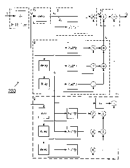
Fig. 10 illustrates a predistorter 200 according to a second embodiment of the
present
invention.This predistorter 200 is based on equation (8) and equation (11)
which is a
generalisation of predistorter 100 given by equation (10). All signal
components correspond
to those signals given by equation (8) and equation (11).
As depicted in Fig. 10. the predistorter 200 according to this second
embodiment includes a
first functional block 1 for generating an estimate
of the drain current id . which
corresponds to the first functional block 1 of the predistorter 100 in fig.
9.. The predistorter
200 further includes a functional block 8 for generating a signal vs as a
function of the
estimate id of the drain cuiTent and gain functions /110 , hi] - hi 2 = which
represent the
sensitivity of the power amplifier and depend on the amplitude of a selected
time-delayed
version v, of the estimate 1d= A further functional block 9 of the
predistorter 200 is arranged
CA 02637228 2008-07-15
19
WO 2007/117187
PCT/SE2006/050065
to generate a signal vs, as a function of a conjugate of the estimate id, and
gain functions /1,0,
Ii,. IL,2, which represent the sensitivity of the power amplifier and depend
on the amplitude
of the selected time-delayed version v3 of the estimate id. The predistorter
200 also
comprises a functional block 7. corresponding to the functional block 7 of the
predistorter
100. for combining the signals v8 and r, to form the output signal r=
Using equation (11), the output signal 1,, can also here be divided into three
signal
components represented in Fig. 10 by signals v, . v8 and r respectively, where
v, folli(,ln¨k1) is the output from the functional block 4 (similar for
both Fig. 9 and Fig_.
10):
. f .
vs = L In] = hi,õ(lid r ¨ k 1) . is the output from the functional
block 8; and
nr.k
= L7. =.=-)
tdr ¨ j= ij[n ¨ 112,õ(lid[n ¨ k 1) is the output from the
functional block 9.
or similarly.
v4 = v3f0 (11'30
V8 = Lid [n ¨ Id = him (IV 31)
ntz-qc
1
V9 = l, [fl¨ mj=v: = h 1)
2rn 3
trrAk
where again, v3 = id[11-1:1
Thus. the output signal vg is given by:
vg V4 + 38 + V9
The predistorter 200 of Fig. 10 differs from the predistorter 100 of Fig. 9 in
the following:
CA 02637228 2008-07-15
WO 2007/117187
PCT/SE2006/050065
The functional block 2 and the functional block 5 in Fig. 9 have been combined
into a
nonlinear FIR filter represented by the functional block 8 in Fig. 10.
The functional block 2 and the functional block 6 in Fig. 9 have been combined
into a
nonlinear FIR filter represented by the functional block 9 in Fig. 10.
5
These combinations may easily be implemented if the functional block 2 of Fig.
9, which is
used to generate the estimate of drain voltage variations given by equation
(9), is realized with
only a few filter coefficients, and if each of these filter coefficients
(constant) is replaced with
the output from a function.
As illustrated in Fig. 10. the functional blocks 8 and 9 include only a few
taps, which is a
further advantage of this embodiment of the invention since relatively few
number of taps are
easier both to implement and to adapt.
Thus. when implementing a predistorter in accordance with the present
invention a trade-off
between efficiency and complexity must be taken into consideration when
choosing the
number of taps. However, a person skilled in the art appreciates that any
number of taps could
be used.
Finally, explicit absolute abs value block in Fig. 9 have been embedded in
function blocks fo
and h.,.
Normally, no tap in functional block 2 of Fig. 9. and functional blocks 8 or 9
of Fig. 10 arc
selected to have the same total delay as functional block 3. This is shown in
the equations
above as well wherein the sums of equations (9). (10), and (11) delay /n is
selected to be
different from a selected delay k (i.e. m # k) . On the other hand, if extra
redundancy is not a
concern this restriction could be ignored.
Fig. 11 illustrates a method for reducing the memory effects in a RF power
amplifier using a
predistorter having an input signal .v and an output signal
according to the second aspect
of the invention.
CA 02637228 2008-07-15
21
WO 2007/117187
PCT/SE2006/050065
At step Si, a first signal component id is generated by estimating a drain
current of the
amplifier using a linear filter.
At step S2. a second signal component v8 is generated as a function of the
first signal
component id and at least one first gain function ko ,Ii , k2,
, which at least one first gain
function ko , hõ, k2, f, represents the sensitivity of the power amplifier
and is a function of
the amplitude of a selected time-delayed version v3 of said first signal
component id.
At step S3, a third signal component v, is generated as a function of a
conjugate of the first
signal component id and at least one second gain function /120, h, h22, L.
which at least
one second gain function km . //21, 112, . t2 represents the sensitivity of
the power amplifier
and is a function of the amplitude of the selected time-delayed version v3 of
said first signal
component id.
Finally, at step S5. an output signal v, is generated and fed to the amplifier
by combining at
step S4 at least the second signal component vs and the third signal component
v, .
Fig. 12 is a schematic block diagram of a third aspect of the invention
wherein a base station
10 including a power amplifier provided with a predistorter in accordance with
the present
invention is illustrated. In Fig. 12 elements that are not necessary for
understanding the
invention have been omitted. such as for instance modulators and D/A
converters, and other
base station components. According to Fig. 12. an input signal x is forwarded
to a
predistorter 20 in accordance with the present invention. The predistorter
output signal v, is
further forwarded to a power amplifier 30. and the amplified signal is fed to
an antenna.
Predistorting the input signal x effectively reduces frequency memory effects
in the power
amplifier in accordance with the present invention.
As mentioned above, a predistorter in accordance with any described embodiment
of the
present invention has the advantage that it can easily be combined with other
prior art
predistorters. Fig. 13 illustrates such a combination 300, where a
predistorter in accordance
with the embodiment of the present invention as shown in Fig.. 10 is combined
with a prior art
CA 02637228 2008-07-15
WO 2007/117187
PCT/SE2006/050065
predistorter as described in the international patent application WO
2004/086607. As depicted
in Fig. 13, the FIR filter Zo has been omitted. In addition, the gain
functions /7100 I (11)
Iii, 11) = h70(I1) = /1-21(11) , 1122 (11) of Fig. I() have been replaced by
look-up-tables LLITs that
take an address as an input. This address is generated in a separate block and
is separately
delayed. The outputs from LUT tables hi , /1h, h2, are here directly deduced
from the
new invention, while functions (10 and a, are deduced from prior art described
in the
international patent application WO 2004/086607. Furthermore, the functional
delay block 3
in Fig,. 9 or in Fig. 10 has been included into the functional blocks 8 and 9
of Fig. 10.
A person skilled in the art appreciates that the predistorter of the present
invention can also be
adaptive since the property of the amplifier could change over time, i.e. the
amplifier's
properties might be affected by factors such as ageing or changes in the
properties of the
amplifier's surroundings and using an adaptive predistorter will prevent any
deterioration of
the amplifier.
As mentioned earlier, an amplifier becomes more sensitive to drain voltage
variations when
the RF drain voltage is close to saturation which for a conventional amplifier
only happens at
peak powers. but for a Doherty amplifier, which has higher efficiency,
saturation happens
much earlier. This is due to the fact that in a Doherty amplifier, only one
drain voltage is close
to saturation making the Doherty amplifier more sensitive to frequency memory
effects at this
drain voltage. Therefore, the predistorter according to the present invention
is particularly
suitable for reducing the effects of variations in the drain voltages for a
Doherty amplifier.
However, the person skilled in the art appreciates that the predistorter of
the present invention
will effectively reduce frequency memory effects in other type of amplifiers.
It is also apparent to a person skilled in the art that the predistorter
according to the present
invention can be realised in many different ways. This predistorter can be
realised in hardware
with means of digital circuits or as software in a signal processing circuit.
CA 02637228 2008-07-15
?:3
WO 2007/117187
PCT/SE2006/050065
Furthermore. although the present invention has been described with reference
to a FIR filter
structure, it is also possible to use the same principles for an IIR (Infinite
Impulse Response)
filter structure. or a combination of FIR and HR filter structures. Thus. the
most 2eneral filter
structure in which the invention may be implemented is a discrete time filter
structure.
It will be understood by those skilled in the art that various modifications
and changes may be
made to the present invention without departure from the scope thereof, which
is defined by
the appended claims.