Note : Les descriptions sont présentées dans la langue officielle dans laquelle elles ont été soumises.
CA 02640990 2008-10-14
PATENT
81088-361486
TI7'LE
PARALLEL GAPPED FERRI7'E CORF,
BACKGROUND OF THE INVENTION
Field of the Invention
[00011 The present invention generally relates to a core utilized in
transformers and
inductors, and in particular to a parallel gapped ferrite core. Transformers
and inductors
utilizing the core of the present invention find applications in various
electronic circuits,
including switching power supplies.
Description of Related Art
100021 Not all of the power input to a transformer or inductor is delivered to
a load
coupled to the inductor or transformer. The difference between the input power
and the output
power is the loss, which is often manifested as heat. Three types of loss are
associated with an
inductor or transformer. They are copper loss, core loss, and fringing loss.
(0003J I'he core loss is dependent on the core material and the flux density
property of
the core material. The core loss is a fixed loss.
[00041 Copper loss is based the AC and DC resistance of the windings. The
copper loss
is related to the current demand of the load to which the inductor or
transformer is coupled. If
the core is an inductor, the AC resistance of the winding assists in
generating the copper loss.
100051 When designing a transformer or inductor core, a gap is utilized to
store energy.
Fringing loss is the blooming of the flux lines across the gap. Energy builds
up in a core and can
be released into the windings of the transformer or the inductor. Fringing
losses (caused by the
fringing flux lines across the gap) cause stray flux lines around the gap.
These stray flux lines
create eddy currents which impinge on the windings of the transformer or
inductor.
Accordingly, it is desired to minimize the fringing loss of the core.
100061 Fig. 1 A illustrates a top perspective view of a core according to the
prior art. The
transformer core includes a I-bar core 110, a printed circuit board 120, and
an E-core 130. The
printed circuit board 120 includes cutouts to allow a center leg 131 and end
sections 132 of the
E-core 130to pass through the circuit board 120 without contacting the circuit
board 120.
100071 Fig. 1 B illustrates a top view of the core of Fig. IA. The I-bar core
110 is
positioned on top of the printed circuit board 120. Fig. 1 C illustrates a
cross-sectional view of
1
6004366191.DOC
CA 02640990 2008-10-14
PATENT
81088-361486
Fig. 1B along the line A-A 112. Referring to Fig. 1C, a gap 135 is formed
between a center leg
131 of an E-core 130 and the I-bar core I 10. The gap 135 may be formed
because a center
section 131 of the E-core 130 has been machined or cut down to ensure there is
no contact
between the center section 131 of the E-core and the 1-bar core 110. The gap
135 allows a core
to carry DC currents and prevent saturation. The gap 135 also sets the
inductance. Fig. 1 D
illustrates magnetic flux lines 150 and 152 in two locations. Fig. I D is a
side cross-sectional
view of the transformer taken across line A'-A'. In a perfect core utilized in
either a transformer
or inductor, the magnetic flux lines 150 travel across the gap 135 as desired.
Flux lines 152 are
fringing flux lines. Instead of traveling straight across the gap 135, the
fringing flux lines 152
fringe out when traveling from the E-core 130 to 1 10. The fringe flux lines
impinge upon the
circuit board 120 at an angle approaching 90 degrees. In other words, the
fringe flux lines are
substantially perpendicular to the circuit board 120 and the windings therein,
thus inducing the
eddy currents. The windings are planar with the circuit board 120 and as
illustrated in Fig. ID,
the fringing flux lines 152 travel in a horizontal direction across the
circuit board 120. These
create eddy currents caused by the fringing flux lines and decrease the
efficiency of the
transformer or inductor.
[0005] Fig. 2A illustrates a top perspective view of a second embodiment of a
transformer core according to the prior art. The core may be referred to as a
distributed gap
core. The distributed gap core 200 may include an I-bar core 210, a spacer
215, a printed circuit
board 220, and an E-core 230. The I-bar core 210 is positioned on top of the
spacer 215 which
is positioned on top of the printed circuit board 220. The printed circuit
board 220 includes
cutouts to allow a center leg 131 and end sections 132 of the E-core 230 to
pass through the
circuit board 220 without contacting the circuit board 220. Fig. 2B
illustrates a top view of the
distributed gap core according to the prior art. Fig. 2B illustrates the
positioning of [-bar core
210, the spacer 215, and the printed circuit board 220 in the distributed gap
core 200. This
confIguration is referred to as a distributed gap core because the spacer 215
fonns a gap between
not only the center leg 231 and the I-bar core 210 but also between the end
sections 232 and the
1-bar core 210. The spacer may be made of a dielectric material or a non-
magnetic material.
100091 Fig. 2C illustrates a side cross-sectional view of the core according
to the prior
art. The cross-sectional view of Fig. 2C is taken along line B-B 223 of Fig.
2B. As illustrated in
Fig. 2C, the [-bar core 210 is positioned on top of the spacer 215 and the
spacer 215 is
positioned on top of the printed circuit board 220. In an embodiment of the
invention, the spacer
215 is also positioned on top of and contacting portions of the E-core 230,
specifically the center
2
600436619 I . DOC
CA 02640990 2008-10-14
PATENT
81088-361486
leg 231. A gap 255 is formed between the E-core 230 and the printed circuit
board 220. 11ie
gap 255 results in magnetic flux lines and fringing flux lines being
generated. Fig. 2D illustrates
fringing flux lines generated by the gap in the distributed gap transformer
core according to the
prior art, Fig. 2D is a cross-sectional view taken along line B'-B' of Fig.
2B. As illustrated in
Fig. 2D, the fringing flux lines 250 generated by the gap 255 travel in a
horizontal direction
across the printed circuit board. The fringing flux lines 250 impinge upon the
circuit board 120
at angle approaching 90 degrees. The fringing flux lines 250 are substantially
perpendicular to
the circuit board and windings therein. These flux lines 250 are generated by
the gap 255
between the I-bar core 210 and the center leg 231 of the E-core 230. As
illustrated in Fig. 2,
there are gaps 265 and 275 created between the end sections 232 of the E-core
230 and the I-bar
core 210. Fringing flux lines are generated by the gaps 265 and 275 and are
represented by
numerals 260 and 270. The fringing flux lines 250, 260 and 270 create eddy
currents in the
windings of the transfonner or inductor. Eddy currents decrease the efficiency
of the windings
in the transfonner or inductor, which result in decreased overall efficiency
of the transformer or
inductor.
3
600436619 1. DOC
CA 02640990 2008-10-14
Aft
PATENT
81088-361486
BRIEF DESCRIPTION OF THE DRAWINGS
100101 Fig. 1 A illustrates a top perspective view of a core according to the
prior art;
100111 Fig_ 1 B illustrates a top view of the core of Fig_ 1 A;
100121 Fig. IC is a side cross-section view taken across line A - A of Fig.
1B;
[0013] Fig. ID illustrates magnetic flux lines generated by a gap in the core;
[00141 Fig. 2A illustrates a top perspective view of a second embodiment of a
core
according to the prior art;
[0015) Fig. 2B illustrates a top view of the distributed gap core of Fig. 2A;
[0016) Fig. 2C illustrates a side cross-sectional view taken across the line B
- B of Fig.
2B;
[0017) Fig. 2D illustrates flux lines generated by a gap in the core of Fig.
2A;
[0018J Fig. 3A illustrates an exploded view of a transformer core according to
an
embodiment of the invention;
[0019) Fig. 3B illustrates a top view of the transformer core of Fig. 3A;
[0020] Fig. 3C illustrates a side cross-sectional view taken across the line C-
- C of Fig.
3B;
[0021) Fig. 3D illustrates flux lines generated by a gap in the core of Fig.
3A;
[0022) Fig. 3E illustrates a top view of a core including variable width gaps
according to
an embodiment of the invention;
100231 Fig. 3F illustrates a side cross-sectional view taken across the line D-
D of Fig.
3E;
[00241 Fig. 4 illustrates a core including a parallel gapped core and
distributed gap core
according to an embodiment of the invention; and
[00251 Figure 5 illustrates a block diagram of a power adapter system with a
transformer
and an inductor utilizing a core of the present invention.
DETAILED DESCRIPTION OF THE INVENTION
[00261 A core, as discussed below, may be utilized in an inductor (i.e., an
inductor core)
or a transformer (i.e., a transformer core). The core may be made of a number
of materials
including alloys, amorphous iron power, manganese-zinc ferrite, molybdenum
permalloy
powder, nickel-zinc ferrite, sendust, and silicon steel. In the description
below, the core may be
referred to as a transformer core, but the description equally applies to an
inductor core.
4
600436619 I . DOC
CA 02640990 2008-10-14
PATENT
81088-361486
100271 In the description below and corresponding drawings, the windings are
described
and illustrated as being disposed on a printed circuit board. The description
equally applies to
other windings that are located or positioned on any surface that is between
two magnetic
elements (e.g., cores, gapping plates, frames, core portions). For example,
the windings may be
formed on a stamped conductor sheets that is placed between two insulating
sheets or the
windings may be wire wrapped around an insulating spool.
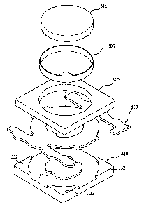
100281 Fig. 3A illustrates an exploded view of a transformer core according to
an
embodiment of the invention. In an embodiment of the invention, the
transformer core includes
a gapping plate 315, a spacer 305, a frame core 310, a printed circuit board
320 and a bottom
core 330. Illustratively, the bottom core 330 may be an E-shaped core. In an
embodiment of the
invention, the frame core 310 may be rectangular- or square-shaped. The frame
core may also
be circular, an oval, a hexagon or other shapes. A portion or section of the
frame core 310 may
be cut out or removed from the frame core. In an embodiment of the invention
illustrated in
Figs 3A and 3B, a circular portion of the frame core 310 is cut out.
100291 In an embodiment of the invention, the gapping plate 315 may be
constructed
from the cutout portion of the frame core 310. In the embodiment of the
invention illustrated in
Fig. 3A, the result is a circular gapping plate 315. Illustratively, the
diameter of the circular
gapping plate 315 may be smaller, by a predetermined amount, than the diameter
of the cutout
part of the frame core 310. This may be created by the enlarging a size of the
hole in the frame
core 310 or by grinding down the edge of the gapping plate 315. A circular gap
is created
between the gapping plate 315 and the frame core 3 10 because of the different
diameter sizes.
In an embodiment of the invention, a spacer 305 may be placed in a portion of
the gap to ensure
that the gapping plate 315 maintains a fixed position with respect to the
frame core 310. The
spacer may be constructed of a dielectric material or a non-magnetic material.
In this
embodiment of the invention, the spacer 305 forms the gap which generates flux
lines and
fringing flux lines. The printed circuit board 320 may include cutouts to
allow a center leg 331
and end sections (or legs) 332 of the E-core to pass through the printed
circuit board 320.
[0030) Fig. 3B illustrates a top view of the transformer core of Fig. 3A. The
gapping
plate 315 is placed inside the cutout of the frame core 310. Both the gapping
plate 315 and
frame core 310 rest on top of the printed circuit board 320. The spacer 305
may fill the gap
between the outer circumference of the gapping plate 315 and the inner
circumference of the
frame core 3 10.
600436619_ i . DOC
CA 02640990 2008-10-14
AML
PATENT
81088-361486
100311 Fig. 3C illustrates a cross-sectional view of the transformer core
around a printed
circuit board according to an embodiment of the present invention. The cross-
section is taken
across line C-C 342 of Fig. 3B. The bottom core 330 is positioned below the
printed circuit
board 320. A center leg 33 1 of the bottom core 330 passes through a cutout in
the printed circuit
board 320. In an embodiment of the invention, the center leg 331 of the bottom
core 330 may
contact the gapping plate 315. In this embodiment of the invention, there is
no gap between the
center leg 331 of the bottom core 330 and the gapping plate 315. Because there
is no gap, there
are no fringing flux lines flowing horizontally across windings on the printed
circuit board 320.
No eddy currents are created and thus the efficiency of the windings is
improved over the prior
art. Under other operating conditions, there may be minimal fringing flux
lines. As illustrated
in Fig. 3C, the gap 350 is a vertical air gap and lies above a portion of the
printed circuit board
340. The gap 350 is an area between the gapping plate 315 and the frame core
330 that exists
after the cutout has been removed. The spacer 305 forms the gap 350. In this
embodiment of
the invention, there is no gap between either the frame core 310 or the
gapping plate 315 and the
printed circuit board 240. Likewise, there is no gap between the printed
circuit board 320 and
the bottom core 330.
[0032] Fig. 3D is a cross-sectional view of the transformer core illustrated
in Figs. 3A,
3B and 3C according to an embodiment of the invention. Fig. 3D is taken across
line C'-C' of
Fig. 3B. As is illustrated in Fig. 3D, there is no gap between the end
sections 332 of the bottom
core 330 and the frame core 310. There is also no gap between the center leg
331 of the bottom
core 330 and the gapping plate 315. A gap 350 exists between the gapping plate
315 and the
frame core 310. As illustrated in Fig. 3D, two gaps 350 exist in this cross-
sectional view, e.g.,
one on the left side of the core and one on the right side of the core.
Fringing flux lines 355
radiate away from the gap(s) 350 in a vertical direction. The fringing flux
lines 355 are
radiating in planes parallel with the windings on the circuit board 320. In
this embodiment of
the invention, vertically radiating fringing flux lines 355 (or parallel
radiating flux lines) do not
interfere with windings on the printed circuit board 320 of the transformer
and do not create
eddy currents. Under other operating conditions, vertically radiating flux
lines 355 interfere
minimally with windings of the printed circuit board 320 of the transformer
and create small
magnitude eddy currents. Accordingly, the windings of the printed circuit
board 320 operate
efficiently and the transformer suffers minimal losses due to fringing loss in
the embodiment of
the invention illustrated in Fig. 3D.
6
600436619 I . DOC
CA 02640990 2008-10-14
PATENT
81088-361486
100331 In an embodiment of the invention, the spacer 305 may be made of
plastic.
Alternatively, the spacer 305 may be made of any non-conductive and non-
magnetic material.
Any suitable insulating material may be utilized to construct the spacer. In
embodiments of the
invention, the thickness of the vertical gap (e.g., vertical gap 350) may be
10 hundredths of an
inch (i.e., 0.010 inches). The thickness may vary depending on the application
in which the core
is utilized and may have a thickness in the range of 0.001 inches to 0.1
inches.
100341 Fig. 3E illustrates a top view of a core embodying the invention with a
variable
width gap according to an embodiment of the invention. Fig. 3E illustrates a
gapping plate 370,
a spacer, fotming gaps 381, 382, 383, and 384, a frame core 380 and a circuit
board 385. As
noted above with regard to Fig. 38, the gapping plate 370 may be rectangular-
or circular-
shaped. Similarly, the frame core 380 may have the shape of an oval, a circle,
a square, a
rectangle, or other shapes. In this embodiment of the invention, the gap
formed by the spacer
375 has a variable width. A core having the variable gap width may be utiiized
in transfotrners
or inductors, such as swinging inductors. Fig. 3E illustrates a spacer having
a thin width 381 on
a top side of the core and a thin width 382 on the left side of the core. The
widths 381 and 382
may be the same dimension or may be different dimensions. The spacer (which is
the gap) 375
has a thicker width 383 on the right hand side of the core and a thicker width
384 on the bottom
side of the core. The widths 383 and 384 are larger in size than the widths
381 and 382. The
widths 383 and 384 may be the same magnitude or may be different magnitudes.
100351 Fig. 3F illustrates a cross-sectional view of a transformer core taken
along a line
D-D of Fig. 3E. The core in Fig. 3F includes the gapping plate 370, the frame
core 380, the
circuit board 385 and the bottom core 390. As is illustrated in Fig. 3F, the
width of the gap 382
is smaller than the width of the gap 383. This results in fringing flux lines
that radiate in parallel
planes from windings on the circuit board. In Fig. 3F, the fringing flux lines
are represented by
reference numerals 391 and 392. In this embodiment of the invention, the
parallel radiating
fringing flux lines 391 and 392 do not interfere with windings on the printed
circuit board 385 in
the core and do not generate eddy currents. Under other operating conditions,
the parallel
radiating fringing flux lines 391 and 392 minimally interfere with the
windings and create small
eddy currents. Accordingly, the windings of the printed circuit board 385
operate efficiently and
the transformer suffers minimal losses due to fringing loss in the embodiment
of the invention
illustrated in Figs 3E and 3F.
[00361 Fig. 4 illustrates a cross-sectional view of a core embodying the
invention and
also embodying the distributed gap topology. In this embodiment of the
invention, gaps 470 are
7
600436619 1. DOC
CA 02640990 2008-10-14
Ask.
PATENT
81088-361486
present between 1) the frame core 410 and the end sections 432 of the bottom
core 430 and 2)
the gapping plate 415 and the center leg 431 of the bottom core. These gaps
470 generate flux
lines 460 that radiate in a horizontal direction across the printed circuit
board 420. Gaps 450 are
also present between the gapping plate 415 and the core frame 410. Gaps 450
create fringing
flux lines 455 which radiate in a plane parallel with the surface of the
circuit board away from
the gap 450. The parallel radiating fringing flux lines do not generate large
eddy currents and
minimally interfere with the operation of the transformer or inductor because
of the small or
non-existent eddy currents that are generated.
100371 The core may be made of a number of pieces. In an embodiment of the
invention, the core may include a number of sections. The core may include a
first magnetic
section, a second magnetic section and a third magnetic section. "The second
magnetic core
section lies above the first magnetic core portion. In this embodiment of the
invention, the
second magnetic core section may have a hole having a first circumference. The
third magnetic
core section lies above the first magnetic core portion. In an embodiment of
the invention, the
third magnetic core section may lie in a plane parallel to or substantially
parallel to the second
magnetic core section. The third magnetic core section has a second
circumference. The second
circumference is less than the first circumference which creates a gap between
the second
magnetic core section and the third magnetic core section. The gap generates
magnetic flux
during operation of the core which results in flux lines and fringing flux
lines. The fringing flux
lines radiate in a direction perpendicular to the first magnetic core section.
These fringing flux
lines radiate in planes parallel to the plane which includes the windings on
the circuit board. In
an embodiment of the invention, the magnetic flux radiates in a direction
perpendicular or
substantially perpendicular to the second magnetic core sections and the third
magnetic core
sections. In an embodiment of the invention, the first magnetic core section
may include a
number of pieces of core material. Illustratively, the first magnetic core
section may include a
center piece and a number of end pieces attached to the base. The center piece
may be located in
a position where the center piece is under the third magnetic core section. In
an embodiment of
the invention, the center piece may contact the third magnetic core section.
100381 Figure 5 illustrates a block diagram for a power adapter 500. An AC
power
source 510 may deliver an AC input voltage. For example, the AC input voltage
may be 90 --
264 Volts AC and may be operating at between 44 and 470 Hz. Altematively, a DC
power
source 520 may deliver a DC voltage. For example, the DC voltage may power
range from 1 I-
16 Volts DC.
8
600436619 1. DOC
CA 02640990 2008-10-14
PATENT
81088-361486
[00391 If the AC input power source 510 is used in a power adapter 500, the AC
power
source 510 may be filtered by utilizing an input EMI filter 525. The EMI
filter 525 rejects both
differential and common mode generated noise. The filtered input voltage
exiting from the EMI
filter 525 is rectified by the input rectifier 530 and may become a haversine
waveform. The
output of the input rectifier 530 is provided to a switching circuit 540. A
control circuit 545 may
control operation of the switching circuit 540. The rectified voltage is
switched to a transformer
550 embodying the invention. The transfonner receives the switched recrified
voltage at the
primary winding 551 and induces current to the secondary winding 553 of the
transformer. The
voltage at the secondary winding 553 is rectified and filtered by a rectifier
555 to provide an
intennediate bus voltage, which is represented by reference number 560.
(0040) The DC power source 560 is used to power a high efficiency voltage
doubler
circuit 575. The voltage doubler circuit 575 may include an auto-transformer
circuit. The
voltage doubler circuit 575 effectively doubles the input voltage to provide
power to the
intermediate bus 560 when operating on the DC input voltage In an embodiment
of the
invention, the voltage doubler circuit 575 (including the auto-transformer
circuit) is included in
a cable 570 connected between the DC power source 520 and the power adapter
body 515.
[00411 The output voltage for the power adapter 500 is provided by a high
efficiency
synchronous buck regulator 580. The buck regulator 580 derives power from the
intermediate
bus 560. The buck regulator 580 may be programmable. The buck regulator 580
may be able to
output a voltage from, for example, 0- 25 volts. This may be referred to as
being capable of
zero up operation.
[00421 While the description above refers to particular embodiments of the
present
invention, it will be understood that many modifications may be made without
departing from
the spirit thereof. The accompanying claims are intended to cover such
modifications as would
fall within the true scope and spirit of the present invention. The presently
disclosed
embodiments are therefore to be considered in all respects as illustrative and
not restrictive, the
scope of the invention being indicated by the appended claims, rather than the
foregoing
description, and all changes which come within the meaning and range of
equivalency of the
claims are therefore intended to be embraced therein.
9
600436619 1 DOC