Note : Les descriptions sont présentées dans la langue officielle dans laquelle elles ont été soumises.
CA 02642258 2013-12-04
METHODS AND SYSTEMS FOR SIMULTANEOUS REAL-TIME MONITORING
OF OPTICAL SIGNALS FROM MULTIPLE SOURCES
STATEMENT REGARDING FEDERALLY SPONSORED RESEARCH
[0001] Portions of this invention were made under NHGRI Grant No. RO1
HG003710-01, and the United States Goverment may have rights to such
inventions.
BACKGROUND OF THE INVENTION
[0002] Optical detection systems are generally employed in a wide variety
of different
analytical operations. For example, simple multi-well plate readers have been
ubiquitously
employed in analyzing optical signals from fluid based reactions that were
being carried out
in the various wells of a multiwell plate. These readers generally monitor the
fluorescence,
luminescence or chromogenic response of the reaction solution that results
from a given
reaction in each of 96, 384 or 1536 different wells of the multiwell plate.
[0003] Other optical detection systems have been developed and widely
used in the
analysis of analytes in other configurations, such as in flowing systems,
i.e., in the capillary
electrophoretic separation of molecular species. Typically, these systems have
included a
fluorescence detection system that directs an excitation light source, e.g., a
laser or laser
diode, at the capillary, and is capable of detecting when a fluorescent or
fluorescently labeled
analyte flows past the detection region (see, e.g., ABI 3700 Sequencing
systems, Agilent 2100
BioAnalyzer and ALP systems, etc.)
[0004] Still other detection systems direct a scanning laser at surface
bound analytes
to determine where, on the surface, the analytes have bound. Such systems are
widely used in
molecular array based systems, where the positional binding of a given
fluorescently labeled
molecule on an array indicates a characteristic of that molecule, e.g.,
complementarity or
binding affinity to a given molecule (See, e.g., U.S. Patent No. 5,578,832).
[0005] Not withstanding the availability of a variety of different types
of optical
detection systems, the development of real-time, highly multiplexed, single
molecule analyses
has given rise to a need for detection systems that are capable of detecting
large numbers of
different events, at relatively high speed, and that are capable of
deconvolving potentially
1
CA 02642258 2013-12-04
. .
s
complex, multi-wavelength signals. The present invention meets these and a
variety of other
needs.
BRIEF SUMMARY OF THE INVENTION
[0006] Various embodiments of this invention provide a method of
monitoring a
plurality of spectrally distinct optical signals from a source of optical
signals, comprising:
passing the plurality of optical signals through an optical system that is
configured to image
each of the plurality of spectrally distinct optical signals onto an imaging
detector that
comprises a plurality of pixels, wherein an image of each spectrally distinct
optical signal has
a shape of an aggregate group of pixels that is characteristic of optical
signal's spectral
characteristics; imaging the plurality of optical signals onto the imaging
detector; and
identifying each optical signal by the shape of the aggregate group of pixels
characteristic of
that optical signal.
[006A] Various embodiments of this invention provide a system for
monitoring a
plurality of different optical signals from a source of optical signals,
comprising: a substrate
having at least a first source of optical signals disposed thereon, the source
of optical signals
including a plurality of spectrally distinct optical signals; an optical
system positioned to
receive the plurality of different optical signals from the at least first
source of optical signals
and differentially image each of the plurality of different optical signals
onto an imaging
detector that comprises a plurality of pixels such that an image of each of
the different optical
signals has a shape of an aggregate group of pixels that is characteristic of
the spectrally
distinct optical signal; an imaging detector; and a processor for processing
signal data from
the imaging detector, wherein the processor is configured to identify the
spectrally distinct
optical signal by the shape of the aggregate group of pixels characteristic of
that optical
signal.
[0007] The present invention is generally directed to systems and
methods for
monitoring a number of different optical signals from a number of different
and discrete
sources of such signals. The methods and systems are particularly useful in
monitoring
chemical and biochemical reactions of interest from an array of reaction
regions on a substrate
where such reactions are taking place. Of particular interest are the use of
these methods and
2
CA 02642258 2013-12-04
systems in such analytical operations involving relatively high speed, low
level signal
generation as is found in single molecule analyses, e.g., in nucleic acid
sequencing reactions.
[0008] In one aspect, the invention provides methods and systems for
monitoring one
or more optical signals from a substrate having at least a first signal source
disposed thereon.
The methods typically comprise imaging the optical signal onto an imaging
detector that
comprises a plurality of pixels. The signal data from a first set of pixels is
then subjected to a
first data process, wherein the first set of pixels correspond to at least a
portion of the imaged
signal. The signal data from a second set of pixels different from the first
set of pixels is
subjected to a second data process different from the first data process. The
output of at least
the first data process is then recorded to monitor the optical signal.
[0009] Relatedly, the systems of this aspect of the invention comprise a
substrate
having at least a first source of optical signals disposed thereon, an optical
train positioned to
receive optical signals from the at least first source of optical signals and
image the optical
signals onto a imaging detector, an imaging detector comprising a plurality of
pixels, the
detector positioned to receive the image of the optical signals on a first set
of pixels in the
plurality of pixels, and a processor programmed to process signal data from
the detector to
monitor the optical signals. In accordance with this aspect of the invention,
at least one of the
detector or processor are configured to process signal data from the first set
of pixels in a first
data process and data from a second set of pixels in the plurality of pixels
different from the
first set of pixels in a second data process different from the first data
process.
[0010] In another aspect, the invention again provides methods and
systems for
monitoring an optical signal from a source of optical signals. The methods of
this aspect of
the invention comprise imaging the optical signal onto a plurality of pixels
on an imaging
detector,
2a
CA 02642258 2008-08-12
WO 2007/095119 PCT/US2007/003570
followed by combining signal data from the plurality of pixels, and processing
the combined
signal data to monitor the optical signal.
[0011] The systems of this aspect typically comprise a substrate having
at least a first
source of optical signals disposed thereon, an optical train positioned to
receive optical signals
from the at least first source of optical signals and image the optical
signals onto an imaging
detector, an imaging detector comprising a first plurality of pixels, the
detector positioned to
receive the image of the optical signals on a second plurality of a pixels in
the first plurality of
pixels, and a processor programmed to process signal data from the detector to
monitor the
optical signals. Again, in this aspect of the invention, at least one of the
imaging detector and
processor are configured to combine signal data from the second plurality of
pixels to provide
combined signal data, and process the combined signal data.
[0012] In another aspect of the invention is provided methods and systems
for
monitoring a plurality of spectrally distinct optical signals from a source of
optical signals. The
methods of this aspect of the invention typically comprise passing the
plurality of optical signals
through an optical train that is configured to image each of the plurality of
spectrally distinct
optical signals onto an imaging detector, wherein an image of each spectrally
distinct optical
signal has an image shape characteristic of its spectral characteristics. The
plurality of optical
signals is then imaged onto the imaging detector. Each optical signal is then
identified by its
characteristic image shape to monitor the plurality of spectrally distinct
optical signals.
[0013] The systems of this aspect of the invention typically comprise a
substrate having
at least a first source of optical signals disposed thereon, the source of
optical signals including
plurality of spectrally distinct optical signals. Also included is an optical
train positioned to
receive the plurality of different optical signals from the at least first
source of optical signals
and differentially image each of the plurality of different optical signals
onto an imaging
detector such that an image of each of the different optical signals is
characteristic of the
spectrally distinct optical signal, an imaging detector, and a processor for
processing signal data
from the imaging detector, wherein the processor is configured to identify the
spectrally distinct
optical signal by its characteristic image shape on the imaging detector.
[0014] In still other aspects, the invention provides methods and systems
for processing
an optical image on an imaging detector from a source of optical signals. The
methods of this
aspect of the invention comprise imaging the optical signal onto an array of
pixels on an
imaging detector. Signal data is then acquired from the plurality of pixels
upon which the
optical signal is imaged. The acquired signal data is then transferred to a
storage region of the
detector, and= subjected to a gain process during the transferring step to
amplify the signal data.
3
CA 02642258 2008-08-12
WO 2007/095119 PCT/US2007/003570
[0015] The systems of this aspect of the invention typically comprise a
substrate having
at least a first source of optical signals disposed thereon. Also included are
an optical train
positioned to receive optical signals from the at least first source of
optical signals and image the
optical signals onto an imaging detector and an imaging detector. Typically,
such imaging
detector includes a plurality of optically active pixels in an image
acquisition portion of the
detector, and a data=storage portion of the detector operably coupled to the
image acquisition
portion to receive signal data from the image acquisition portion in a frame
transfer process.
The detector is configured to apply a gain voltage to the signal data during
the frame transfer
process to amplify the signal data transferred to the data storage portion of
the detector.
[0016] In another aspect, the invention provides methods, detectors and
systems useful
in monitoring optical signals. The methods of this aspect of the invention
comprise imaging the
optical signals onto an imaging detector that comprises a plurality of pixels.
Signal data from
the plurality of pixels that falls within a selected signal amplitude range is
then selected, and is
subjected to a gain protocol to amplify the selected signal data, while not
amplifying signal data
that was not selected.
[0017] Relatedly, the invention provides an imaging detector for carrying
out the
foregoing method. The detector typically includes a plurality of optically
active pixels in an
image acquisition portion of the detector, a data storage portion of the
detector operably coupled
to the image acquisition portion to receive signal data from the image
acquisition portion in a
frame transfer process, and a gain register operably coupled to the data
storage portion to
amplify signal data from the data storage portion. The detector is configured
to pass signal data
through the gain register that falls within a selected signal amplitude range.
[0018] The invention also provides methods and systems for monitoring
optical signals
where the system comprises a source of optical signals, an optical train
positioned to receive the
optical signals from the source of optical signals and image the optical
signals onto an imaging
detector, and an imaging detector positioned to receive imaged optical signals
onto a plurality of
optically sensitive pixels that are operably coupled to a gain register to
amplify signal data from
the plurality of pixels. The method typically comprises measuring a gain
from the gain
register in the absence of an imaged optical signal on the plurality of
optical signals.
[0019] In yet another aspect, the invention provides methods of
monitoring a plurality of
spectrally different optical signals from a single signal source. These
methods typically
comprise collecting the spectrally.different optical signals in an optical
train. The spectrally
different optical signals are then transmitted through the optical train that
is configured to
differentially image each of the spectrally different optical signals onto an
imaging detector.
4
CA 02642258 2008-08-12
WO 2007/095119 PCT/US2007/003570
Each spectrally different signal imaged upon the detector is then identified
by its image on the
imaging detector.
[0020] In other aspects, the invention provides methods of monitoring
optical signals
from a plurality of signal sources on a substrate, that comprise imaging the
plurality of signal
sources onto an imaging detector that comprises a plurality of pixels, wherein
images of the
plurality of signal sources are directed substantially onto a first subset of
the plurality of pixels,
but not substantially on a second subset of the plurality of pixels. The
signal data from the first
subset of pixels but not from the second subset of pixels are then subjected
to further data
processing to monitor signals from the plurality of signal sources.
[0021] Also provided are methods of monitoring one or more signals from a
signal
source, comprising: imaging a first optical signal onto a first plurality of
pixels on an imaging
detector; selecting from the first plurality of pixels a first subset pixels
that meet or exceed a
signal quality threshold; and processing data from the first subset of pixels
to monitor the one or
more signals from the signal source.
[0022] Other methods of the invention for monitoring one or more optical
signals from
one or more discrete signal sources, comprise: imaging the one or more signals
onto a plurality
of pixels on a detector array; selecting a subset of the plurality of pixels;
recording data from the
subset of the plurality of pixels as indicative of the one or more signals;
correlating the data to a
signal from the discrete signal source.
[0023] In still other methods of the invention, a plurality of optical
signals from one or
more discrete signal sources are monitored. These methods comprise imaging the
plurality of
signals onto a detector array, wherein each signal is imaged onto a plurality
of pixels on the
detector array; and processing data from the plurality of pixels while
discarding data from pixels
not in the plurality of pixels.
[0024] The invention also includes systems that comprise: an array of
optical signal
sources, each signal source being capable of emitting a plurality of signals
having different
optical wavelengths; an optical train for collecting the signals from the
array of signal sources
and differentially imaging each of the plurality of signals having different
optical wavelengths
onto a detector; and a detector for detecting the signals imaged thereon.
[0025] The invention is also directed to systems, that comprise an array
of a plurality of
optical signal sources, the plurality of optical signal sources having a
plurality of spectrally
resolvable fluorescent compounds associated therewith. The system also
includes a source of
excitation radiation, a detector array, and an optical train that is
configured to direct excitation =
radiation from the source of excitation radiation to the array of signal
sources, receive emitted
fluorescent signals from the array of signal sources, and image the
fluorescent signals onto the
CA 02642258 2008-08-12
WO 2007/095119 PCT/US2007/003570
detector array, wherein the optical train is characterized by a dichroic
filter in optical
communication with an objective lens, wherein the dichroic filter is
reflective of the fluorescent
signals and transmissive to the excitation radiation.
[0026] In still additional aspects, the invention provides methods for
resolvably detecting
a plurality of spectrally different optical signals from at least a first
signal source, comprising:
collecting the plurality of spectrally different optical signals from the
signal source; and
differentially imaging each of the spectrally different optical signals on a
detector array, such
that each different signal is resolvably detected.
[0027] Relatedly, the invention also provides methods of monitoring an
optical signal
from a signal source, comprising: imaging the optical signal onto a plurality
of pixels of a
detector array in a signal image; selecting a subset of the plurality of
pixels in the signal image
having a higher signal intensity within the signal image than other pixels
within the signal
image; and measuring the signal in the subset of pixels.
[0028] Also provided herein are methods of monitoring signals from a
plurality of signal
sources, comprising: imaging each of the plurality of signals onto a detector
array comprising a
plurality of rows and columns of pixels; processing data derived from pixels
in rows or columns
upon which the plurality of signals is imaged, but not from rows of pixels
upon which no signal
is imaged.
[0029] Other methods of the invention for processing signals imaged onto
an EMCCD,
comprise: determining whether the signals imaged onto the EMCCD are within a
preselected
signal amplitude range; and processing only signals that are within the
preselected aniplitude
range through a gain register on the EMCCD.
[0030] In still other methods of processing signals imaged onto a CCD
that is configured
to transfer image data acquired by the detector to a storage region on the CCD
in a frame
transfer process, an elevated voltage is applied to the frame transfer process
to amplify signal
data being transferred.
[0031] In a further aspect, the invention provides systems for monitoring
optical signals
from a plurality of sources of optical signals, comprising: an atm)/ of
discrete sources of optical
signals, said discrete sources emitting optical signals having different
spectral characteristics; an
excitation radiation source; a detector array; an optical train configured to:
direct excitation
radiation from the source of excitation radiation to the array of discrete
sources; receive emitted
optical signals from the array of signal sources; and differentially image the
optical signals
having different spectral characteristics onto a detector array; and a
processor configured to
record the optical signals imaged onto the detector array and correlate the
optical signals with a
property of or an event occurring within the sources of optical signals.
6
CA 02642258 2008-08-12
WO 2007/095119 PCT/US2007/003570
BRIEF DESCRIPTION OF THE DRAWINGS
[0032] Figure 1 is a schematic illustration of an overall system the
present invention.
[0033] Figure 2 provides a schematic illustration of an array of signal
sources on a
substrate, such as zero mode waveguides.
[0034] Figure 3 provides a schematic illustration of an alternative
spacing and/or
orientation scheme for an array of signal sources, in accordance with certain
aspects of the
invention.
[0035] Figure 4 is a schematic illustration of one example of a mounting
stage
configured to receive and support substrates bearing signal sources for
analysis in the systems of
the invention.
[0036] Figure 5 is a schematic representation of an x-y-z translation
robotic system for
translating one or more of the substrate and/or the optical train relative to
the other, within the
systems of the invention.
[0037] Figure 6 schematically illustrates the substrate and optical train
of the systems of
the invention that includes optical componentry for the separation and
detection of spectrally
resolvable signal components.
[0038] Figure 7 provides a schematic illustration of a system of the
present invention
that includes optical componentry for simultaneous illumination of larger
numbers of signal
sources on the substrates.
[0039] Figure 8 provides a schematic illustration of a multiple
excitation source/multiple
emission wavelength system that utilizes transmissive fluorescence optics.
[0040] Figure 9 provides a schematic illustration of a multiple
excitation source/multiple
emission wavelength system that utilizes reflective fluorescence optics.
[0041] Figure 10 provides a block diagram illustrating the operation of
an EMCCD
detector and data processing steps of certain aspect s of the invention.
[0042] Figure 11 provides a comparative illustration of signal image
correlation methods
from a detector array that take into account optical aberrations in the
upstream optical train.
[0043] Figure 12 schematically illustrates a comparison of data
extraction processes in
conventional image processing versus processes employed in certain aspects of
the invention.
[0044] Figure 13A and B schematically illustrate pixel correlation to
imaged signals or
signal components to improve the fidelity of data from a given image or set of
images.
[0045] Figure 1z.1- schematically illustrates data management on an EMCCD
detector to
enhance efficiencies of the system.
7
CA 02642258 2008-08-12
WO 2007/095119 PCT/US2007/003570
[0046] Figure 15 provides a flowchart of data processing from CCD
detector arrays to
minimize effects of large signal variations.
DETAILED DESCRIPTION OF THE INVENTION
I. Introduction
[0047] The present invention is generally directed to optical detection
or monitoring
systems, methods enabled by such systems, and components of such systems for
monitoring, in
real-time, optical signals that emanate from multiple discrete sources of
those optical signals. In
particular, the optical detection and monitoring systems of the invention are
generally capable of
monitoring discrete signals from potentially very large numbers of different
signal sources,
optionally separating_and/or deconvolving such signals into constituent signal
events, and doing
so in real-time, despite that such signals may be changing rapidly, over time.
[0048] The systems of the invention thus include all or a portion of a
collection of
different functional elements. These elements include the multiple discrete
sources that include
the capability of generating optical signals. In preferred aspects, such
sources include chemical,
biochemical and/or biological reactants, or mimics of such reactants that are
capable of
generating optical signals that are indicative of their presence, reaction or
conversion. While the
sources may be capable of generating optical signals on their own, in
preferred cases, a source of
excitation radiation is also provided to excite optical signals, e.g.,
fluorescence, within the
sources.
[0049] The systems of the invention also typically include optical
elements that direct,
separate, and/or otherwise alter optical signals from these sources (as well
as excitation radiation
directed at such sources), in order to ultimately derive optimal amounts of
information from
such signals when they are ultimately detected. Consequently, the systems of
the invention
typically include an optical detection system for detecting the potentially
large numbers of
signals that were directed from the sources, and optionally separated and/or
otherwise altered by
the optical elements.
[0050] Signals detected by the optical detection system are then recorded
and processed
by appropriate processing systems and data management processes to provide
output of the
system in user ready formats.
[0051] As alluded to previously, the systems of the invention are
preferably applied in
the monitoring of arrays or collections of spatially discrete chemical,
biochemical and/or
biological reactions that generate optically detectable signals, such as
chromogenic reactions,
luminescent or luminogenic reactions, or fluorescent or fluorogenic reactions.
A few examples
of preferred reactions include those that are regularly performed in the
pharmaceutical,
8
CA 02642258 2008-08-12
WO 2007/095119 PCT/US2007/003570
biotechnology and healthcare diagnostic fields, i.e., immunoassays, enzymatic
assays, receptor
assays, nucleic acid hybridization assays, nucleic acid synthesis reactions,
cellular assays, and
many others.
[0052] Typically, the progress of the reactions used in application of
the systems
described herein result in one or more of the consumption, production and/or
conversion of a
material that is capable of generating an optically detectable signal, either
alone, or in response
to an external stimulus, e.g., excitation radiation. By way of example,
certain reactants may
become fluorescent upon reaction with another reactant, or may have their
fluorescence altered
or reduced upon such reaction. As such, the fluorescence emitted from the
reaction in response
to an excitation radiation will change as the reaction progresses. The systems
of the invention
provide for the source of such signals, e.g., the area in which the reaction
occurs, including
optionally, the reactants and/or products, the optical elements for
collecting, directing and
optionally separating andJor altering such signals from such sources, and the
ultimate detection
of such signals, as well as the manipulation of the resulting data to yield
optimal value and
information for the user.
[0053] The systems of the invention typically include all or a subset
of a substrate that
includes all or a subset of the sources of optical signals, an optional
excitation light source, an
= optical train that includes the various optical elements for collection,
direction and/or
manipulation of the optical signals and optional excitation light, optical
detectors for receiving,
detecting and recording (or putting into a form for recordation) the optical
signals, as well as
processors for processing data derived from the optical detectors.
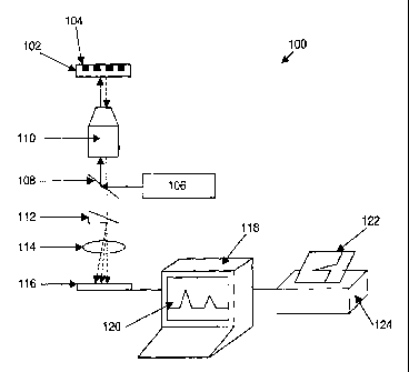
[0054] A general schematic representation of the system as set forth
above, is illustrated
in Figure 1. As shown, the system 100 includes a substrate 102 that includes a
plurality of
discrete sources of optical signals, e.g., reaction wells or optical
confinements 104. An
excitation light source, e.g., laser 106, is optionally provided in the system
and is positioned to
direct excitation radiation at the various signal sources. This is typically
done by directing
excitation radiation at or through appropriate optical components, e.g.,
dichroic 108 and
objective lens 110, that direct the excitation radiation at the substrate 102,
and particularly the
signal sources 104. Emitted signals from source 104 are then collected by the
optical
components, e.g., objective 110, and passed through additional optical
elements, e.g., dichroic
108, prism 112 and lens 114, until they are directed to and impinge upon an
optical detection
system, e.g., detector array 116. The signals are then detected by detector
array 116, and the
data from that detection is transmitted to an appropriate data processing
unit, e.g., computer
118, where the data is subjected to interpretation, analysis, and ultimately
presented in a user
ready format, e.g., on display 120, or printout 122, from printer 124.
9
CA 02642258 2008-08-12
WO 2007/095119 PCT/US2007/003570
[0055] The various functions, applications and components of the systems
of the
invention are set forth in greater detail below.
11. Substrate
A. Substrate
[0056] As alluded to previously, the substrates of the invention, as a
general matter,
provide the multiple discrete sources of optical signals. In the case of
systems for monitoring
reactions, such signal sources typically comprise discrete regions in which
reactions are taking
place and from which discrete optical signals may emanate. In a broad sense,
such different
regions may comprise reaction wells, or zones that are maintained discrete
from other regions by
any of a number of different mechanisms, including chemical or physical
confinements. Merely
by way of example, such regions may comprise discrete patches or zones of
immobilized
molecules on a surface of the substrate, such as in nucleic acid, protein,
antibody or other
immuno-arrays, where the reaction being monitored is the association of
analytes with such
immobilized molecules, they may include channels within a substrate, e.g.,
microfluidic channel
regions, aggregations of capillaries or multiple regions within individual
capillaries, or the like.
[0057] Alternatively or additionally, such regions may include structural
confinements
that maintain the reaction components within the discrete regions. Such
structural confinements
may include wells, depressions, channels, or other structures that retain
reaction constituents.
Such confinements may also include other barriers that effectively provide
structural
confinement through, e.g., the use of chemical barriers, e.g., hydrophobic
regions surrounding
hydrophilic regions on- the substrate surface to retain aqueous reaction
constituents within the
hydrophilic regions.
[0058] In still other aspects, such regions may include combinations of
the above, e.g.,
including immobilized reactants within structural confinements. In addition to
structural
confinements, the reaction regions may comprise optical confinements that may
function as or in
addition to structural confinements on the substrates, that serve to minimize
observation
volumes on the substrate through the confinement of excitation illumination
and/or the
collection of emitted optical signals from relatively small areas or volumes
at the reaction
region. Such optical confinements may include, e.g., waveguides, such as zero
mode
waveguides, optical gratings, optical coatings or the like, that can yield the
excitation or
observation volumes desired on the reaction regions on the substrates.
[0059] Typically, the substrates will comprise an optically transparent
layer upon which
are disposed the reaction regions that provide the discrete sources of optical
signals. The
optically transparent layer may generally comprise any of a number of
transparent solid
CA 02642258 2013-12-04
materials, depending upon other components of the substrate. Such materials
include inorganic
materials, such as glass, quartz, fused silica, and the like. Alternatively,
such materials may include
organic materials, such as polymeric substrates such as polystyrene,
polypropylene, polyethylene,
polymethylmethacrylate (PMMA), and the like, where PMMA is particularly useful
in fluorescent or
fluorogenic reactions, as it has relatively low autofluorescence.
[00601 In preferred aspects, the substrates include zero mode waveguides
as the optical
confinements to define the discrete reaction regions on the substrate. Zero
mode waveguides have
been described in, e.g., U.S. Patent No. 6,917,726. Briefly, such waveguides
comprise a core disposed
through a cladding layer, which in the case of applications to reactions,
comprises an aperture
disposed through the cladding layer that can receive the reactants to be
monitored. Typically, the
aperture has at least one cross-sectional dimension, e.g., diameter, which is
sufficiently small that light
entering the waveguide is prevented in some measure from propagating through
the core, effectively
resulting in a very small portion of the core and its contents being
illuminated, and/or emitting optical
signals that exit the core. In the case of optical signals (and excitation
radiation), the waveguide cores
will typically be between 1 nm and 200 nm, and are preferably between about 10
and 100 nm, and
more preferably between about 30 and about 100 nm in diameter.
[0061] Optical confinements are typically provided upon the substrate in
an array format
where a plurality of confinements are provided upon the substrate. In
accordance with the invention,
arrays of confinements, e.g., zero mode waveguides, are provided in arrays of
more than 100, more
than 1000, more than 10,000, or even more than 100,000 separate waveguides on
a single substrate. In
addition, the waveguide arrays typically comprise a relatively high density of
waveguides on the
surface of the substrate. Such high density typically includes waveguides
present at a density of
greater than 10 zero mode waveguides per mm2, preferably, greater than 100
waveguides per mm2 of
substrate surface area, and more preferably, greater than 500 or even 1000
waveguides per mm2 and
in many cases up to or greater than 100,000 waveguides per mm2. Although in
many cases, the
waveguides in the array are spaced in a regular pattern, e.g., in 2, 5, 10,
25, 50 or 100 or more rows
and/or columns of regularly spaced waveguides in a given array, in certain
preferred cases, there are
advantages to providing the organization of waveguides in an array deviating
from a standard row
and/or column format.
[00621 Optical systems often include a number of optical aberrations,
including, e.g.,
astigmatism, chromatic aberrations, coma, distortion, field curvature, and
spherical aberration. In
many instances, these optical aberrations become more pronounced as a function
off distance from the
axial center of the optical imaging system, such that the magnitude of the
aberration
11
CA 02642258 2008-08-12
WO 2007/095119 PCT/US2007/003570
varies as a function of field position. Accordingly, the optical image is
typically most free of
aberrations at or near the center of the object field, and is more distorted
at the periphery of the
object field and system pupil. Because of such aberrations, resolution and
accurate monitoring
of arrays of discrete nanometer or micron scale sources of optical signals
that are provided in a
relatively high density becomes increasingly problematic away from the center
of the object
field. Consequently, performing analyses in a highly multiplexed array of
waveguides or other
signal sources becomes more difficult.
[0063] In accordance with one aspect of the invention, therefore, the
sources of discrete
optical signals, e.g., the optical confinements, i.e., zero mode waveguides,
in array formats, are
arranged within the array in a non-regular format, to account to minimize the
impact of these
expected optical aberrations, and as a result permit more effective
multiplexed analyses. In
particular, individual sources of signal in the array may be positioned to
account for reduced
resolution, e.g., between neighboring sources, as a function of distance from
the center of the
object image. Additionally, or alternatively, the discrete sources may be
dimensioned to account
for reduced resolution and accuracy at the periphery of the object field. The
variance in optical
resolution, or conversely, aberration, as a function of distance from the
center of the object field
are particularly noteworthy in systems that rely upon imaging based detection
systems, e.g., that
effectively image an entire array or region of an array, that includes
multiple different signal
sources. Examples of such systems include detector arrays, such as diode
arrays, CCDs, i.e.,
ICCDs and EMCCDs, and/or CMOS based image sensors, where signals are detected
at
individual or small groups of pixels on the detector. For example, in CCD
based detectors, as
signals become more distorted away from the axial center of the imaging
system, it becomes
increasingly difficult to assign pixel areas on the CCD that correspond to a
given signal source
in the array of signal sources.
[0064] Figures 2 and 3 show a comparative illustration of arrays of
sources of optical
signals. Figure 2 shows an array 200 of sources of optical signals (shown as
an array of zero
mode waveguides 204 in a substrate 202) that includes regularly spaced and
consistently sized
sources of optical signals. As noted previously, in some cases the sources at
the periphery of the
array, e.g., sources 206 and 208 would be less resolved, optically, than,
e.g., sources 210 and
212. In some cases, it may be the case that aberrations could be sufficient to
prevent resolution
of the peripheral sources, e.g., 206 and 208. Accordingly, as shown in Figure
3, an array 300 of
sources 302 is provided where the spacing between adjacent sources is
increased as a function of
the distance from the center of the object image. For example, as shown,
signal sources that are
nearer the center of the object field represented by the array 300, e.g.,
sources 304 and 306 are
closer together in at least one dimension, than are sources that further away
from the center of
12
CA 02642258 2008-08-12
WO 2007/095119 PCT/US2007/003570
=
the object field, e.g., sources 308 and 310, which are more widely spaced in
at least one
dimension than the more central signal sources. Thus, the space, in at least
one dimension
between two sources at a first distance from the center of the object field of
the optical system
will be less than the space, again in at least one dimension, between two
sources that are at a
second, greater distance from the center of the object field. The spacing
between adjacent signal
sources may be varied in only one dimension, e.g., varied from left to right,
but not from top to
bottom, or it may be varied in both dimensions. In the case where the spacing
is varied in both
dimensions, it will be appreciated that the distance between any two signal
sources at the center
of the object field, e.g., is less than the space between any two signal
sources further away from
the center, i.e., on the periphery, of the object field. The foregoing permits
greater effective
multiplex analysis of arrays of signal sources, such as ZWIVVs.
[0065] Additional arrangements of array elements can be specifically
tailored to fit a
particular aberration of particular optical systems. For example, if a
dominant optical aberration
forms a resulting image spot size or shape that is dependant upon field
location, then that size or
shape can be accommodated in the design of the array of sources by, e.g.,
appropriately spacing
the sources to avoid overlap in image of adjacent sources, or the like.
Similarly, if the shape of
an imaged source is distorted in one dimension so as to potentially overlap
with images of
neighboring sources, that source can be dimensioned to reduce that dimension
and avoid the
overlap, e.g., providing elliptical or rectangular sources.
[0066] In a simpler aspect, the signal sources may also be spaced to
account for optical
manipulations of the signals emanating therefrom. For example, as discussed in
greater detail
below, in some cases, optical signals are spatially separated into component
elements, e.g., light
of different wavelength ranges, indicative of different signaling elements,
i.e., fluorescent
reagents having differing emission spectra. In such cases, it may be desirable
to provide
sufficient spacing between adjacent signal sources on the substrate to prevent
overlap of the
spatially separated signals derived from those sources, when those separated
signals are incident
upon the detector, as set forth below. In this case, increased spacing may
only be required in
one dimension, e.g., providing sufficient spacing between rows of signal
sources, but not
necessarily between the columns of signal sources in the array. Alternatively,
such additional
spacing may be provided in two dimensions. In the case of arrays of signal
sources where the
signals are subjected to spatial separation before detection, such spacing
between adjacent signal
sources may generally range from about 0.1 pm to about 10 pm or more, and is
preferably from
about 0.8pm to about 3 pm or more.
B. Substrate Interface
13
CA 02642258 2008-08-12
WO 2007/095119 PCT/US2007/003570
[0067] The substrates of the invention are typically interfaced with the
overall system
through an appropriate mounting stage that secures the substrate, provides
translational
capability to the substrate, e.g., relative to the optical system, and
optionally provides additional
functionalities, e.g., fluidic interfaces, thermal regulation, e.g., heating
or cooling, positional
registration, and the like. The mounting stage will also typically include a
positioning element
that ensures proper positioning and/or orientation of a substrate upon the
stage, for subsequent
analysis. Such positioning systems may keyed structures on the substrate that
are
complementary to a corresponding structure on the mounting stage. These may
include simple
structures, e.g., tooth/notch structures, truncated comer structures, or other
distinctive and
complementary structures. Alternatively, the keying elements may include
electronic keys, such
as metal contacts and associated electronic components on the substrate and
mounting stage, that
indicate when a substrate is positioned properly and in the correct
orientation for subsequent
analysis. Such key elements may be provided encoded for each substrate, e.g.,
through
incorporated memory elements on the substrate, or through the position and
orientation of
electrical contacts, to indicate a specific substrate, e.g., lot number, etc.
Such identification
systems may provide an ability to ascertain whether a given substrate has been
used previously,
and to what effect. Typically, the mounting stage includes a well or recessed
component
configured to receive the substrate or the packaged structure containing the
substrate, e.g., a
multiwell plate format, as well as a biasing mechanism, e.g., spring, clip or
other mechanism, for
forcibly retaining the substrate in a fixed position on the stage.
[0068] One example of a mounting stage is shown in Figure 4. As shown,
the mounting
stage 400 includes a platform 402 having a mounting region 404 that receives
the substrate (not
shown). The mounting region is typically disposed over an aperture 406 in the
platform 402 that
allows observation of the substrate from underneath. Also as shown, the
mounting stage
includes structures that facilitate the positioning and alignment of the
substrate on the platform.
These may include, e.g., ridges 406, recesses or wells, for positioning the
substrate, and
alignment structures 408, such as pins, bevel structures, tabs, or the like,
that correspond to a
complementary structure on the substrate, e.g., holes or notches. As noted
above, securing
mechanisms may also be provided for locking the substrate in place, such as
biasing mechanism
410, shown as a clip or a closable cover element, shown also from a side view.
Additional
components may be provided on the mounting stage, such as a heating or cooling
element,
additional optical components, and other interfacing elements.
[0069] The mounting stage is also typically coupled to a translation
system for moving
trhe stage in two or three dimensions relative to the optical system. The
translation system
allows scanning of the entire array of signal sources on a substrate, as well
as providing an
14
CA 02642258 2008-08-12
WO 2007/095119 PCT/US2007/003570
ability to move the substrate toward or away from the optical system for,
e.g., focusing, removal
of the substrate, addition of components to the substrate, or the like. A
variety of x-y-z
translation systems are readily available. Additionally, robotic systems are
readily available for
automating the translation functions of the mounting stage in accordance with
preprogrammed
instructions. Figure 5 shows a schematic representation of an entire system
500 including a
schematically represented translation system 502 coupled to a mounting stage
504, supporting
substrate 506 over optical train 508. As shown, the robotic system includes
the capability to
move the substrate in any of the x, y, or z dimensions.
[0070] Robotic systems may also include components that position
substrates upon the
mounting stage, apply reagents to the substrates, and the like. A wide variety
of such robotic
systems that may be applied to the present invention are generally
commercially available from,
e.g., Tecan, Inc., Caliper Life Sciences, Inc., Beckman, Inc., and the like.
111. Excitation Source
[0071] As noted previously, in preferred applications, the systems of the
invention are
used to monitor luminescent or fluorescent signals emanating form the
plurality of discrete
signal sources. As such, in many cases, the systems of the invention include a
source of
excitation radiation. Excitation light sources will generally depend upon the
nature of excitation
radiation needed for a particular application, e.g., as dictated by the
reagents and configuration
of a given analysis. For example, the light source may include lamps, e.g.,
halogen, Mercury,
Xenon, or the like, LEDs, lasers, laser diodes, or any other light source
capable of directing
electromagnetic radiation of a desired excitation wavelength or wavelength
range, to the signal
sources on the substrate. In preferred aspects, lasers are preferred as the
excitation radiation
source, due to the coherency and intensity of radiation that they generate in
desired excitation
wavelength ranges. A variety of different laser types are generally useful for
these applications,
and include, e.g., ion lasers, solid state direct diode lasers, diode-pumped
solid state lasers
(DPSS); solid state frequency converted crystal lasers, and the like. In some
cases multiple
sources may be employed in order to provide multiple different excitation
wavelengths. By way
of example, in cases where the signal sources include fluorescent compounds,
e.g., compounds
labeled with fluorescent dyes, multiple different excitation sources may be
provided for the
various different excitation spectra for such compounds. For example, in the
case of compounds
labeled with A1exa648 dyes, it will typically be desirable to provide at least
an excitation source
that provides excitation radiation range that includes light at the 648 nm,
the respective
excitation wavelengths for these dyes, or if not provided at the nominal peak
of the dye
absorbtion curve, the lasers will include sufficient absorbtion efficiency for
the dyes used, such
CA 02642258 2008-08-12
WO 2007/095119 PCT/US2007/003570
as for A1exa546, where the peak absorption efficiency is closer to 561 nm. In
the cases of
multiple different dyes, different lasers, e.g., having different wavelength
ranges may be used.
IV. Optical Train
[0072] As noted previously, the overall systems of the invention
typically include an
optical train for the direction of excitation radiation to the substrate and
the plurality of signal
sources thereon, and/or for directing emitted signals from these sources to a
detection system
that quantifies and records the signal from each signal source. The optical
trains used in the
overall systems described herein typically include a number of different
optical components for
use in focusing, directing, splitting, separating, polarizing, and/or
collimating the excitation
radiation and/or the signals emanating from the discrete sources of signals.
[0073] A schematic illustration of one optical train is shown in Figure
6. As shown, the
optical train includes an objective lens 602 that is proximal to the substrate
604;and which
focuses excitation radiation, e.g., from laser 606, upon a desired location of
the substrate, and
collects emitted optical signals from the substrate. The optical train will
also typically include
= one or more dichroic mirrors/filters 608, that selectively reflect or
pass excitation light and
emitted optical signals, to effectively separate signal radiation from
reflected or otherwise errant
excitation radiation.
[0074] The optical train may also optionally include signal separation
optics, e.g., to
separate optical signals of different wavelengths or direct them to different
locations on a
detection system. For example, the optical train may include prism 610 that
receives the optical
signs as from the signal sources, that may include signals of several
different primary
wavelengths. Alternatively, sets of dichroic filters may be used in a
cascading arrangement, to
selectively direct each different spectral signal component to a different
detector or detector
region.
[0075] In the case of a prism as a separation element, upon passing
through the prism
610, the different wavelength signals are diffracted to different degrees, and
as a result, are
directed, optionally through additional optical components, i.e., imaging lens
612, at different
angles toward the detection system, e.g., detector array 614 allowing for
their separate detection
and quantitation.
[0076] The ability to separate such signals is of particular value in
monitoring signal
sources that include multiple different reagents that each have a different
fluorescent emission
spectrum, indicative of a different specific reagent, reaction and/or
interaction. A variety of
other optical components may be employed in spectrally separating the optical
signals, including
cutoff filter sets, dichroics, optical gratings, and the like. Such components
will typically be
16
.....
CA 02642258 2008-08-12
WO 2007/095119 PCT/US2007/003570
arranged to direct different portions of each optical signal to different
detectors or, preferably,
different locations upon the same detector or array of detectors. In
accordance with the
invention, different signals may be spectrally resolved by differentially
imaging such signal
components onto the detector, e.g., detector array 614. Such differential
imaging may be
entirely spatially distinct, e.g., by being directed to different detectors or
locations on the same
detector, or they may conformationally distinct, e.g., providing an imaged
signal that is of a
different shape than an image of a different signal component, such that it
can be resolved. For
ease of discussion, both shall be generally referred to herein as being
spatially resolved or
separated or directed to different or regions of the detector, although in
some cases, such
different regions will be understood to overlap.
[00771 Other components that separate portions of the optical signals are
also optionally
included in the optical train, depending upon the application to which the
system is to be put,
including spatial filters, e.g., to confine the optical signals that are
directed to the detector,
polarizing filters, to pass signals that are in one polar optical plane, or
the like. For example, in
addition to separation of signals of differing wavelengths, the optical train
may also include
splitters, e.g., beam splitters, optical gratings, lens or microlens arrays,
and the like, that serve to
divide up the excitation radiation and/or the emitted signals to direct it to
different locations, or
other optical components that change the spatial configuration of excitation
radiation, e.g.,
optional optical grating 616. In some cases, additional filters may be added
after the laser to
filter the main laser line by removing or reducing any optical noise that may
be inherent in the
laser, as well as in front of the detectors to reduce or remove any unwanted
stray light that may
be generated or reflected from the system as a whole, or the ambient light.
[0078] In particular, in certain aspects, one or-more of the optical
train and/or the
excitation radiation source may be configured so as to provide excitation
illumination of a large
number of discrete signal sources on the substrate simultaneously. In the case
of arrays of zero
mode waveguides, for example, the optical train and/or the excitation
radiation source provide
illumination to a large number of zero mode waveguides, simultaneously. As
noted below, the
optical trains are also typically capable of collecting and detecting signals
from the same or
similar large numbers of the signal sources, or in this example, zero mode
waveguides. The
systems typically illuminate at least 2 signal sources, simultaneously,
preferably, greater than 10
signal sources simultaneously, and more preferably, greater than 100 signal
sources,
simultaneously. In some cases, it may be desirable to use the systems
described herein, for the
excitation of 1000, 10,000 or more discrete signal sources. Systems that split
excitation beams
or apply multiple excitation sources (both with or without beam splitting) are
particularly useful
for directing excitation radiation to larger numbers of signal sources.
17
CA 02642258 2008-08-12
WO 2007/095119 PCT/US2007/003570
[0079] Simultaneous illumination with excitation radiation over large
numbers of signal
sources may generally be accomplished through a variety of different means, as
noted above.
For example, one may focus a relatively large spot size upon a large array of
signal sources.
However, as will be appreciated, because laser power is limited, and
indiscriminate illumination
may cause certain adverse effects, e.g., heating, it may be desirable to avoid
illuminating non-
signal generating portions of the substrate. Additionally, in many cases, the
non-signal
generating regions of the substrate may provide additional noise through
reflection of the laser
light. For example, in the case of arrays of zero mode waveguides using a thin
film metal
cladding layer, spaces between signal generating regions are highly
reflective. Such reflected
activation radiation gives rise to elevated noise levels for the system.
[0080] In some cases, larger excitation regions may be provided by
directing multiple
different excitation sources at a given substrate to provide illumination of
larger numbers of
signal sources, e.g., laser 606 and optional additional lasers, e.g., as shown
in Figures 8 and 9.
Unfortunately, use of multiple different sources may provide issues regarding
differences
between the individual sources, e.g., wavelength, frequency or intensity of
illumination that may
impact the signals resulting therefrom, e.g., rendering slightly different
signal profiles.
Additionally, such multiple excitation source systems may still give rise to
the problems of
excessive illumination of the substrate, as a whole. Similarly, excitation
light beams may be
divided into multiple beams, e.g., using beam splitters, optical gratings or
other optical
components, as alluded to above, to direct multiple discrete excitation
illumination spots at
different locations of the substrate, and as a result, illuminating larger
numbers of signal sources
thereon. In a related aspect, lenses may be provided that stretch the beam
spot into an elliptical
or elongated spot shape.
[0081) In certain preferred arrangements, individual or multiple
excitation radiation
source(s) may be manipulated to provide preferential illumination on the
signal sources on a
substrate, and reduce or eliminate illumination at regions of the substrate
not occupied by the
signal source(s). A number of methods may be used to modulate the illumination
profile of the
excitation light source to preferentially provide excitation illumination at
the signal sources on
the substrate, and, in particularly preferred aspects, less illumination at
the spaces not occupied
by such signal sources. In general, this is accomplished by using optical
elements that provide a
signal profile at the object plane of the optical train, e.g., the substrate,
that peaks in intensity at
positions in the object plane that correspond to the position of the signal
sources on the
substrate. A variety of different optical elements may be used to achieve this
illumination
profile. For example, where illumination at a low frequency is not an issue
for analysis of the
signal sources, one may simply employ reciprocating beam, e.g., through the
use of a galvo-
18
CA 02642258 2008-08-12
WO 2007/095119 PCT/US2007/003570
equipped laser system. In cases where low frequency illumination is or can be
an issue, one may
employ holographic or diffractive optical elements to achieve the desired
illumination profile,
e.g., in rows of lines, grids, or the like.
[0082] In particularly preferred aspects, cylindrical lenses or
microlenses, or arrays of
cylindrical lenses or microlenses are used to modulate the excitation light to
provide
illumination in a linear format so as to preferentially illuminate regions
that include signal
sources, and do not illuminate regions of the substrate that include no signal
sources. Further,
such optical elements may yield excitation illumination profiles on the
substrate in multiple
lines, i.e., in parallel and/or in orthogonal orientation, e.g., as a grid, or
the like. For purposes of
discussion, and with reference to direction at the substrate and included
arrays of signal sources,
the "laser spot" or "excitation radiation spot" refers to any of a variety of
different beam shapes,
configurations and orientations that are incident upon the substrate,
including ellipses, lines,
grids, and the like. As will be appreciated, when selectively directing
excitation radiation at the
signal sources on the substrate, the system may be equipped with certain
alignment tools to
facilitate alignment of the excitation radiation with the arrays of signal
sources on the substrate.
Such tools may include reference positions on the substrate that may be
identified, either
manually or automatically, by the system, to orient and/or focus the system
appropriately on the
array of signal sources on the substrate.
[0083] A schematic illustration of this aspect of the invention is shown
in Figure 7. As
shown, the excitation illumination portion of an overall system 700 includes
the excitation light
source, e.g., laser 702, that is directed through an appropriate optical
element, here shown as an
array of cylindrical lenses 704, to an appropriate dichroic mirror, e.g.,
dichroic 706, which
directs the excitation radiation (shown as solid arrows) up through objective
lens 720 and toward
substrate 710. As noted previously, the spatial profile of the excitation
radiation is configured to
preferentially provide greater excitation radiation at the various signal
sources 708 on the
substrate 710, which is in the focal plane of the objective lens 720. An
alternate view of
substrate 710 shows the illumination profile as a series of parallel
illumination regions on the
substrate (as indicated by the dashed outlines 712).
[0084] As described elsewhere, herein, the emitted fluorescence or other
optical signals
from the signal sources, are then collected by objective 720, passed through
dichroic 706, and
are optionally subjected to spectral separation of the signal components,
e.g., via prism 714, and
ultimately directed to a detector, e.g., detector array 718. In addition to
the various optical
components already discussed, the optical trains of the systems described
herein may also
include one or more imaging lenses, e.g., lens 716, to provide a resolved
image of the separated,
and directed optical signals onto an image plane of, e.g., a detector array
718.
19
CA 02642258 2008-08-12
WO 2007/095119 PCT/US2007/003570
[0085] While linear laser or illumination "spots" are preferably aligned
to be collinear
with rows and/or columns of spatially arrayed signal sources, it will be
appreciated that such
illumination lines may be provided at an angle that is offset from the linear
arrangement of the
signal sources, but still illuminating multiple different signal sources
simultaneously. In
particular, by offsetting the illumination lines by a selected angle, one can
still ensure that
illumination of multiple regularly arrayed or gridded signal sources are
illuminated. In its
simplest form, for example, an illuminatio-n line rotated at 45 from the
linear arrangement of
signal sources in a grid will still illuminate those signal sources that lie
on the diagonal.
Similarly, as with regularly spaced rows of crops passed by on the adjoining
roads, numerous
specific angles provide linear arrangements of adjacent signal sources. As
will be appreciated,
the angles that provide effective illumination across multiple different
signal sources in a
gridded array format will generally depend upon the spacing of the sources in
each dimension.
For regularly spaced sources, e.g., equally spaced in two dimensions, for
example, lines at 00,
22.5 , 45 ,-67.5 and 90 angles from the row or column orientation of the
gridded array of signal
sources will generally run parallel to lines that include multiple sources. A
number of angles
between these will likewise provide illumination of multiple sources.
[0086] The various components of the optical train, e.g., lenses,
gratings, filters, prisms,
beam splitters, and the like, are generally obtainable commercially from
optics suppliers,
including, for example, Special Optics, Inc., Newport Corporation, Thorlabs,
Inc., CVI Lasers,
Lambda Research Optics, Lambda Physics, and Precision Optical, Inc.
[0087] In some aspects, the optical train for use in the systems of the
present invention
utilizes a configuration based upon reflective fluorescence filters that more
readily permit
implementation of multi-light source, e.g., laser, excitation systems, that
may be useful for
multi-fluorophore systems, e.g., signal sources that include multiple
different fluorophores in
generating the signals.
[0088] In conventional fluorescence detection schemes, interference
filters are typically
employed that reflect excitation light at an angle of approximately 900 such
that is incident upon
the fluorescent sample, and transmit fluorescent light emitted from that
sample such that its
wave-front remains relatively undisturbed. While the degree of rejected
excitation light
attainable in such transmissive fluorescence geometries is sufficient for most
one or two
excitation band applications, these current schemes may not be effectively
extended to three or
four excitation band schemes, as a single transmissive-fluorescence filter
that efficiently passes
substantial portions of multiple, e.g.õ 2, 3, 4 or more, different fluorescent
spectra while
reflecting the multiple excitation bands, is not readily manufacturable using
available
technology. Further, while multiple filter components could be combined to
achieve this in a
CA 02642258 2008-08-12
WO 2007/095119 PCT/US2007/003570
multiple laser, multiple emission wavelength system, increased transmission
losses, increased
optical aberrations, increased size, and increased costs for making higher
performance
fluorescence transmissive filter systems, make such solutions less desirable.
[0089] In contrast, the optical trains of certain preferred
configurations of the systems of
the invention utilize a reflective fluorescence filter setup-in selectively
directing emitted light to
the detector while blocking excitation light that is reflected from the
substrate or other
components in the system. In particular, the optical trains of this aspect of
the invention
typically include at least one optical filter component that reflects emitted
fluorescent light from
the substrate to direct it to a detector, rather than passing such light. The
systems of the
invention include a multi-band reflective dichroic filter that selectively
reflects multiple emitted
fluorescent wavelength ranges, e.g., emitted by multiple different fluorescent
materials having
distinct emission spectra. In addition to their multi-band reflectivity, these
filter components are
typically capable of passing excitation light (light at the desired excitation
wavelength). As
such, the multi-band dichroic are tailored to transmit excitation radiation at
multiple different
wavelengths, while generally reflecting the longer wavelength emitted
fluorescence. The
dichroics are further tailored to include relatively narrow reflective ranges,
so as to permit
transmission of excitation bands that fall between or among two or more
emission bands. Such
reflective fluorescence systems benefit from superior performance dichroics,
as compared to the
transmissive dichroics, and also have cost and simplicity benefits.
[0090] Because the narrow-band selectivity is applied in reflection
versus transmission,
more of the reflected excitation radiation is filtered by being transmitted
through the multi-band
dichroic, and not reflected. To the extent that any excitation radiation is
reflected by the
multiband dichroic, it can be selectively filtered out following separation of
the individual
excitation spectra (also referred to as 'color separation'), using an
individual narrow-band notch
filter that is applied to one separated color (e.g., one selected emission
spectrum), as all colors or
emission spectra. As a result, any transmission losses are only applied to an
individual
spectrum, and not over the entire emission spectra. Further, fabrication of a
single multi-narrow
band reflective filter is more readily achievable using available technology
than a narrow multi-
band transmissive filter.
[0091] Figures 8 and 9 provide schematic illustrations of conventional
fluorescence =
transmissive optical trains and the fluorescence reflective optical trains of
the invention. For
ease of discussion, components that are common among the two configurations
are given the
same reference numbers. As shown in Figure 8, a fluorescence transmissive
optical train 800
includes at least a first excitation light source, e.g., laser 806. For multi-
band excitation, one or
more additional light sources, e.g., lasers 802 and 804 are optionally
included. Where such
21
CA 02642258 2008-08-12
WO 2007/095119 PCT/US2007/003570
additional light sources are included, they are typically coupled with and
directed at dichroic
filters, e.g., dichroics 808, 810 and 812, respectively, so that all of the
excitation radiation from
the various sources is co-directed, as indicated by the solid arrows. The
excitation light is then
directed at a multiband dichroic filter 814 that reflects substantially all of
the excitation radiation
at the substrate 816 that is being subjected to analysis. Fluorescent signals
emitted from the
substrate or sample surface are then passed through the multiband dichroic
814, which is
transmissive to light at the wavelengths of the emitted fluorescence, along
with some portion of
reflected excitation radiation. In the case of multiple different fluorescent
emission spectra, the
emitted fluorescence is then subjected to a color separation step, where the
different individual
emission spectra are separated from each other and separately detected. Color
separation may
be accomplished using a series of cascaded dichroic filters, such as filters
818, 820, and 822
whereby a selected emission spectra is reflected from each of the dichroics
onto an adjacent
detector 832, 834 and 836, respectively, with the last emission spectrum
transmitting through all
of the dichroics to be incident onto detector 838). Alternatively, a prism
based color separation
process may be employed where different emission spectra are directed through
an appropriate
optical grating or prism to spatially separate the individual spectra and
direct them to different
detectors or different regions on an array detector. Additional filter
elements, e.g., notch filters
824-830 may be included within the optical train to further tailor the
emission radiation detected
at each of the detectors, e.g., to filter out any inadvertent reflected
excitation or emission light.
As will be appreciated additional lasers, e.g., fourth fifth, etc. lasers, may
be included in the
system with the concomitant inclusion of additional optical elements, e.g.,
filters, dichroics, etc.
[0092] In contrast, Figure 9 provides a schematic illustration of a
fluorescence reflective
optical train, in accordance with certain aspects of the invention. As shown,
although in a
different orientation, the system includes similar excitation light sources
(e.g., lasers 802-806)
and dichroics (808-812) to codirect the excitation radition. However, in
contrast to Figure 8, the
excitation light is directed at and transmitted, rather than reflected by
multi-band dichroic 902,
which is tailored to be reflective of multiple, narrow bands of emitted
fluorescence. The
excitation radiation is then transmitted, rather than reflected, by dichroic
902. Emitted
fluorescence is then reflected, rather than transmitted by dichroic 902, and
then subjected to
optional separation and detection, e.g., in a similar manner to that shown in
Figure 8. As will
be appreciated, although the dichroics are shown oriented at 45 angles in the
system to reflect
light, e.g., fluorescence as in Figure 9, at 900 angles relative to its angle
of incidence, in some
cases it may be desirable to reflect the light at greater than a 90 angle,
e.g., rotating the dichroic
so that the angle of incidence of both the transmitted excitation light and
emitted fluorescence is
22
CA 02642258 2008-08-12
WO 2007/095119 PCT/US2007/003570
shallower than 45 , as such higher reflectance angles provide for
simplification in dichroic
fabrication.
[0093] The optical train included in the systems of the invention also
may include an
autofocus function for automatically adjusting the objective or other lenses
in the optical system
to focus the sample material being analyzed within the focal plane of the
optical train. A variety
of different autofocus systems may generally be incorporated into the systems
of the invention.
[0094] As noted elsewhere herein, the optical trains of the invention,
whether based
upon fluorescence transmission or reflectance, typically directs the emitted,
and preferably
separated, fluorescent signals to a detector. In particularly preferred
aspects, the detector
comprises an array of point detectors, such as a diode array detector or a
charge coupled device
(CCD, ICCD or EMCCD). In the case of such array detectors, it may be desirable
for the optical
train to provide the directed fluorescence onto the detector in a particular
desired 'configuration.
For example, in some cases, it is desirable to image a fluorescent signal onto
a plurality of pixels
that exceeds a minimum threshold level. For example, providing sufficient
signal data from at
least 2 pixels, preferably at least 4 pixels, and more preferably at least 10,
20 or even 100 pixels
may be desirable to provide for enhanced statistical evaluation of data. In
accordance with this
aspect of the invention, the data from these multiple pixels will typically be
combined before or
during the processing of the signal data therefrom. In some cases, the signal
data from the
selected pixels would be averaged and/or subject to correction, e.g., for
background signal or
noise, in order to provide optimal statistical confidence in a given data. In
still other cases, the
data may be combined prior to substantive processing, in order to reduce the
data load that is
subjected to the various processing steps, e.g., in a gain register or other
processing system. In
particular, and as described in greater detail below, like data, e.g.,
corresponding to a single
signal or to background or quiet pixels, may be co-processed in order to
minimize the amount of
individual data units that are subject to such processing, and thus reduce the
processing
requirements of the overall system.
[0095] In the case of signals having multiple, separated spectral
components, it may be
desirable to image each different fluorescent signal component, e.g., each
differently colored
spot of emitted fluorescence, onto a plurality of pixels of an array detector,
so that variations in
intensity across an individual signal spot may be accommodated in data
analysis, e.g., averaged,
discarded, etc. For example, in many cases, each signal component will be
imaged on at least
two pixels in a detector array, preferably at least 4 or more pixels in the
detector array, and in
some cases upwards of 10, 20 or 50 or more pixels.
[0096] In the case of signal sources, e.g., sample substrates that
include an array of
discrete signal sources, the total number of pixels involved in detection of a
given spectral signal
23
CA 02642258 2008-08-12
WO 2007/095119 PCT/US2007/003570
from the overall array will typically vary approximately by the multiple of
the sources being
analyzed. For example, if each separated color signal from each discrete
signal source on an
array is imaged onto 4 pixels in the detector array, and 10 signal sources
were being analyzed
using the same array, then the aggregate signal for that color for the entire
array of signal
sources would be imaged onto approximately 40 pixels of the detector array. As
has been
reiterated herein, in particularly preferred aspects, the imaged signal will
typically include at
least two separated spectral components, and preferably 3, 4 or more spectral
components that
are directed to and imaged upon different detectors or regions on a detector
array, utilizing a
range of numbers of pixels.
V. Detector
[0097] The systems ofthe invention may generally include any of a
variety of different
detector types useful for detecting optical signals that are directed to the
detector. Examples of
different types of detectors include photodiodes, avalanche photodiodes,
photomultiplier tubes,
imaging detectors, such as charge coupled devices, CMOS (complementary metal
oxide
semiconductor) sensors or imagers, CCD/CMOS hybrid imagers, and the like. In
preferred
aspects, imaging detectors are employed in the systems of the invention, so as
to provide
simultaneous detection over larger areas of the substrates, and consequently,
larger numbers of
discrete signal sources. Charge coupled device based detectors (CCDs) and CMOS
image
sensors are particularly preferred for their ability to simultaneously detect
and/or monitor signals
from large numbers of discrete signal sources on the substrate. Because data
derived from these
types of image or imaging detectors is assigned to discrete pixels, signals
from discrete sources
that are incident upon different locations of the detector may be separately
detected and
quantified. Further, in applications where relatively high speed, and
relatively low signal levels
are prevalent, e.g., where the signal sources comprise single molecule type
reactions, highly
sensitive detectors are generally preferred, such as electron multiplying CCDs
(EMCCD) or
intensified CCDs (ICCD). Typically, EMCCDs are preferred for their sensitivity
to low signal
levels.
[0098] Figure 10 provides a schematic illustration of the operation of
an exemplary
EMCCD in processing image data. As shown, an overall system 1000 includes a
typical
EMCCD chip 1002, which has an image area 1004 and a storage area 1006. The CCD
includes
an EM gain register 1008 that is operably connected to an appropriate
analog:digital converter
1010, which is, in turn, connected to a processor or computer, e.g., computer
1012. As shown,
. each area comprises a 512X512 pixel array. As shown in step A, an image
is acquired (Step A)
(Frame 1) in the image area 1004 and transferred to the storage area 1006
(step B) so that the
24
CA 02642258 2008-08-12
WO 2007/095119 PCT/US2007/003570
image area is available for acquiring subsequent images, e.g., Frame 2 (Step
C). In the case of
some EMCCDs, the frame transfer requires an applied potential of approximately
2V. The
frame in the storage area (Frame 1, as shown) is then transferred into the EM
Gain register 1008
pipeline (step D) (again, requiring approximately 2V), where the charge
associated with the
image is passed through approximately 536 stages to achieve a potential gain
range, that is
software controllable, from 1 to of 2000X. The EM gain register processing
typically requires
approximately 50V. The amplified image data is then passed through an analog
to digital
converter 1010 (step E) to be stored or further processed by a computer 1012
(step F).
[00991 As with the illumination of signal sources, in preferred aspects,
the detection
systems in the systems of the invention are typically capable of detecting
and/or monitoring
signals from at least 2 different signal sources, simultaneously, preferably,
at least 10 discrete
signal sources, and in many cases, more than 100 or even more than 1000
discrete signal
sources, simultaneously. Further, the detectors are likewise capable of
monitoring or detecting
multiple, spatially separated signals or signal components from each such
source. In particular,
as noted above, signals from each discrete source are preferably spatially
separated, at least
partially, into at least two, and preferably, three, four or even more
separate signal components,
that are directed onto the detector array and are capable of resolution and
ultimately being
separately detected. In some cases, two different signals that may be emitted
from a given signal
source may not be completely spatially separable onto different regions of a
detector array.
However, because such signals differ in their emission wavelength spectra,
subjecting such
different signals to the wavelength separation components of the optical
train, e.g., a prism such
as prism 610 in Figure 6, can yield imaged signals on a detector array that
have imaged shapes
that are characteristic of the particular emission spectrum, while not being
completely spatially
separable from another signal components having slightly different emission
spectra. In such
cases, identifying the signal component that gives rise to a detectable event
can sometimes
include identification of a characteristic shape of an aggregate group of
pixels upon which such
signal is incident. As will be appreciated, in those cases that utilize
detector arrays as image
detectors, e.g., CCDs, CMOS sensors, and the like, detection of image shape
will typically refer
to detection of signals at the various detector elements, or pixels, that are
reflective of an imaged
signal of a given shape. Thus, identifying a signals imaged shape will
generally refer to
detection of signal at pixels underlying that image shape, rather than
holistically identifying the
shape. Further, the identification of the signal component based upon the
imaged shape may not
specifically include a step where the shape is identified, but rather that
signal is detected that is
characteristic of that shape. Thus, with respect to these methods,
identification of image shape
CA 02642258 2008-08-12
WO 2007/095119 PCT/US2007/003570
may not include any step whereby the shape is actually identified, e.g.,
"shape is circular", but
may only be identified by the identification of the pixels upon which the
signal is incident.
VI. Data Management
(00100] The systems of the invention also typically include a data
processing system
coupled to the detector for processing and/or recording signals that are
incident upon and
detected by the detector, and for processing that data to useful information
for the user. For
example, in the case of single molecule analyses, e.g., where the signal
source comprises
fluorogenic reactants, the data processing system may assign a value to the
incidence of signal
on a given location of the detector at a particular time, as being indicative
of the occurrence of a
given reaction. The data derived from each signal would typically include one
or more of (a) the
intensity of the signal, (b) the pixel or pixels upon which the signal was
incident, (c) relative
time that the signal was detected, and the like. Such data may then be
processed to indicate
relative rates or activities of reactants, order of reactions, a particular
signal source from which
the signal was derived, and through knowledge of that source's reactants, the
nature of an
analyte exposed to such reactants.
[001011 For ease of discussion, where the signal source includes template
directed DNA
synthesis using fluorescent nucleotide analogs and DNA polymerase enzyme
within an optical
confinement, a signal may be indicative of the incorporation of a nucleotide
at a given relative
position in the synthesis. Further, using the spectral separation aspects of
the optical train, and
four different nucleotide analogs all bearing dyes or labels having resolvably
different spectral
characteristics, e.g., that are separated by the optical train and directed to
different locations on
the detector (or that possess different imaged shapes) as a result of their
differing spectral
characteristics, a signal at a given location on the detector (or having a
given shape) can be
indicative of incorporation of a specific type of analog, and the relative
timing of such signal
would be indicative that such base occurs in the template sequence before or
after another base
which gave rise to an earlier or later signal, respectively. Finally, the
location on the array
where such signals are incident is indicative of the signal source from which
the signals derive
(e.g., indicating that subsequent signals at the same approximate location
(subject to, e.g., spatial
separation based upon spectral differences of components of signals from a
given source) are
likely a result of the continuation of the same reaction). This detection is
repeated multiple
times to identify the sequence of incorporation of multiple nucleotides. By
virtue of the
complementarity of incorporation in template directed DNA synthesis, one may
then ascertain
the underlying sequence of nucleotides in the template sequence.
26
CA 02642258 2008-08-12
WO 2007/095119 PCT/US2007/003570
[001.02] In at least one aspect, as with the aspects of the invention that
adjust the array of
sources depending upon expected optical aberrations, one may also adjust the
methods by which
data is acquired and/or assigned to individual sources, based upon those
expected optical
aberrations. In particular, as noted previously, an amount of distortion of an
imaged array can
increase as a function of distance from the axial center of the object field.
As a result,
correlating or assigning individual pixels or groups of pixels to a specific
signal source in an
imaged array becomes more difficult away from the center of the image.
Additionally, optical
aberrations may further deform the shape of the imaged signal depending upon
the position on
the detector array of the imaged signal. For example, certain optical
aberrations, i.e., coma, may
yield an imaged signal from a circular source that is 'tear-drop' shaped,
falling away from the
axial center of the imaged field. Alternatively, combinations of astigmatism
and field curvature
could result in an elliptical signal image shape from a circular signal
source, which is more
pronounced with increasing distance from the axial center of the object field.
(001031 Accordingly, in at least one aspect, one can accommodate
increasing levels of
distortion by expanding the number of pixels that are correlated to any given
source, in
conjunction with a known or expected optical aberration of the system. In a
simple form, this
involves increasing the number of pixels correlated to a given source being
imaged as that image
(or its respective image source) is farther away from the center of the image
or object field. A
schematic illustration of this is shown in Figure 11. As shown, an array of
pixels in an array
detector, e.g., a CCD 1100, is provided to image the array of signal sources.
As shown in panel
A, in the absence of optical aberrations, uniform signal sources yield uniform
images upon the
CCD, e.g., as indicated by signals 1102-1112, regardless of where in the image
field they
emanated from. However, in the case of systems sensitive to such optical
aberrations, as the
distance increases between the center of the imaged field and a given imaged
source, e.g.,
moving from imaged spots 1120 and 1122 to spot 1124, the distortion results in
increasing
image size, and/or lower resolution. In order to account for this distortion,
the pixels correlated
to a given image or signal are increased to maximize the data acquired for
each imaged signal,
e.g., by acquiring as much of the given signal as possible or practicable,
e.g., including all of the
different pixel regions at the center and periphery of the object field,
imaged onto the CCD.
The adjustment of correlated or recorded pixels for any given signal image is
a particularly
useful process when combined with an array of sources that is further arranged
to account for
such optical aberrations, e.g., see Figure 3, above. Alternatively, or
additionally, and also as
shown in Figure 11, one may adjust the assigned pixels for a particular imaged
signal to account
for distortions in the shape of the imaged signal, e.g., for an elliptical or
tear-drop shaped image.
27
CA 02642258 2008-08-12
WO 2007/095119 PCT/US2007/003570
In particular, one may employ a collection of pixels for an individual imaged
signal that is larger
in one axis than the other, e.g., longer in the y axis as shown in Figure II.
[00104] In addition to the improved ability to separately monitor signals
from discrete
sources, the use of such CCD or other array detectors provides additional
benefits for analysis of
signals from the individual signal sources as well as the aggregate signals
from the overall array
of signal sources. For example, where a signal from a given discrete source is
incident upon
multiple pixels, the compartmentalization of data on a pixel basis allows
selection of optimal
pixels in a given imaged signal, for data analysis, e.g., eliminating edge
signals that may have
higher levels of noise or distortion. Additionally or alternatively, pixels
used to obtain signal
data for each discrete signal source may be individually tailored for a
variety of different
purposes, as discussed elsewhere herein. The management of such pixel data is
further
described in greater detail below.
[00105] In addition to accommodating and/or correcting for optical
aberrations, the
present invention also provides processes that provide more efficient
processing of relevant
signals. In at least one general aspect, such processes involve the further
processing of only
relevant signals, while either discarding or combining less relevant signals.
In either case, by
reducing the amount of signal data that is subjected to the full range of
further processing, one
can speed up that processing, reduce processing requirements, e.g., computing
power, reduce
real estate on an array detector required for image data management, extend
the lifespan of
detector components, and achieve a variety of other benefits. These processes
generally may be
carried out either in the context of the CCD chip, or they may be performed in
a subsequent, off-
chip processes, e.g., using a computer. As will be appreciated, in many cases,
preferred
implementations are carried out within the image data processing steps on the
detector array
itself.
[001061 In the context of the present invention, it will generally be
understood that the
term "processing" refers to automated processing of data by a mechanical or
solid state
processor or system that is programmed to carry out such processes, e.g., in
machine readable
software or firmware. Thus, the processing steps may be carried out by a
single solid state
device, e.g., an appropriately configured detector chip such as an EMCCD, or
by a connected or
integrated computer or other processor.
[00107] As alluded to above, in certain aspects, the invention provides
for an initial data
processing or selection step to avoid the management, storage and/or
processing of excessive
irrelevant data that is or would be produced by the detection system, as well
as the combined
processing of certain data from different areas on the detector. In
particular, in some cases, one
may gain significant advantages, e.g., in terms of speed of data processing
and management and
28
CA 02642258 2008-08-12
WO 2007/095119 PCT/US2007/003570
usefulness of background signal data, through the selective skipping,
removing, or combining of
pixel data prior or subsequent to extraction of data, e.g., from a CCD chip.
Stated in another
way, by ignoring or separately processing data collected from certain pixel
areas that do not
contain highly relevant data, e.g., they fall outside of a relevant imaged
signal, one can speed up
the data management process by removing large amounts of irrelevant data from
the process or
combining into one processible unit, all of the background or less relevant
signal data.
Additionally, or altennatively, such combined less relevant pixel data may be
useful to derive
more meaningful background signal levels, or noise, of the system. In either
case, the speed and
accuracy of the system should benefit.
[00108] By way of example, where one is imaging a large number of discrete
signal
sources or separated signals derived from such sources, on a single detector
array, e.g., a CCD,
ICCD or EMCCD, space between imaged signals from such discrete sources gives
rise to little
or no useful data, as it is a "quiet" space. Notwithstanding the lack of
useful signal data
emanating from these regions of the detector array, the data from such
locations has typically
been recorded, e.g., as a zero, or some other low level signal value, or other
irrelevant value.
While such signals can be disregarded as background, their recordation and
processing to the
point of discard still requires memory space for storage and processing
capacity for evaluation
and ultimate discard. Accordingly, in certain aspects, the invention provides
a masking process
for filtering out such quiet locations on the detector array, and thus
blocking the data from being
recorded.
[00109] For example, in a first aspect, rows of detector array elements,
such as pixels in
CCD based detectors, that fall between rows of imaged signals from the
discrete signal sources,
and thus carry signals that are not as relevant to the desired analysis, may
be skipped during data
extraction from the detector arrays. Figure 12 provides a schematic
illustration of this data
extraction profile in a CCD array. As shown, individual signals 1204 from
signal sources (not
shown) are imaged onto an array detector, e.g., CCD 1202. As shown, the imaged
signals 1204
are imaged upon rows of pixels 1206 that are interspersed with rows of pixels
1208 upon which
no relevant signals are being imaged, also generally referred to as "quiet
pixels". As will be
appreciated, within each row of pixels 1206 upon which are imaged relevant
signals, there may
exist quiet pixels between each individual imaged signal element, e.g., pixels
1210. For ease of
illustration and discussion, the extraction of data from pixel rows and/or
columns is generally
illustrated with respect to pairs of adjacent rows and/or columns, rather than
from individual
pixel rows, but such illustration is not indicative of any process requirement
or other parameter.
[00110] In a typical image extraction process, all of rows 1206 and 1208
would be
subjected to the same processing steps, resulting in a substantial amount of
resources being
29-
CA 02642258 2008-08-12
WO 2007/095119 PCT/US2007/003570
dedicated to the processing of the less relevant or quiet pixels. This is
schematically illustrated
by the arrows emanating from each pixel row (or pair of pixel rows, as shown),
e.g., relevant
signal rows 1206 and quiet pixel rows 1208.
[00111] In accordance with certain aspects of the invention, and as shown
in the image in
panel B, however, data is extracted from the pixels, e.g., the rows and/or
columns that carry
imaged signals, e.g., rows 1206, from an array of signal sources, while the
intervening rows
and/or columns, e.g., rows 1208 (and optionally quiet pixel columns that
include, e.g., pixel
regions 1210) are ignored from a data extraction standpoint. This is shown in
Figure 12, panel
B.
[00112] In particular, as shown, an application of the process would
involve skipping
extraction of data from rows 1208, while extracting data from rows 1206. While
data from the
analyzed rows is subjected to further processing, e.g., passed through EM gain
register and/or
the analog-digital converter (ADC), to the computer or processor for
subsequent storage and
manipulation, the skipped rows are not. This effectively reduces the amount of
data that is run
through the ADC by more than half, in the example shown. Alternatively or
additionally, the
data derived from rows 1208 may be separately combined and/or averaged prior
to or
subsequent to extraction (shown by the dashed arrow in panel B) to provide a
more significant
determination of background noise levels of the system, which may then be used
to further
correct the signal data extracted from, e.g., rows 1206. Even with such
processing of the quiet
pixel data, by binning this data together for processing in a single
processible data unit, the
efficiencies described above are largely retained.
[00113] In other aspects, data from related array elements may be combined
or "binned"
before being subsequently processed, in order to minimize the number of
separate data elements
that are subject to processing. For example, with reference to the extracted
row data described
above, each set of rows and/or columns that corresponds to a particular signal
source image, or
the space between imaged signal sources, may be separately binned for
subsequent processing,
reducing the number of data elements that are subjected to processing.
Similarly, pixels
corresponding to images from individual signal source array elements may be
binned together
and processed. In each of the foregoing cases, whether alone or in
combination, the overall
number of data elements is substantially reduced over the extraction and
processing of each
individual pixel element.
[00114] In addition to providing benefits of data management selectively
binning pixels
of imaged signal components may provide advantages of data analysis. For
example, when
imaging spatially separated signal components, one can selectively bin those
elements that are
derived from signal rows that are of similar -fidelity, allowing subsequent
identification of lower
CA 02642258 2008-08-12
WO 2007/095119 PCT/US2007/003570
fidelity signals, in aggregate. As noted previously, in certain embodiments,
the constituent
elements of each signal, e.g., the different signal wavelengths emanating from
each signal
source, are subjected to spatial separation and are imaged onto different
pixels, or collections of
pixels, on the detector array. As will be appreciated, because constituent
signal wavelengths
tend to fall over a range rather than within a precise single wavelength or
wavelength range in
some cases, and because addition of more signal wavelength components within
the signal
sources as may occur with various applications and/or multiplexing, spatial
separation may yield
less than complete separation between different signal constituents along each
row, e.g.,
resulting in spectral overlap of the separated signals.
[00115} In accordance with certain aspects of the invention, data that is
of higher fidelity
is processed separately than lower fidelity data, even within an imaged
signal. In its simplest
sense, only pixels that correspond to the highest fidelity data, e.g., having
the highest intensity
relative to a noise level of the system, are processed as relevant signals.
Other signal
components are then subjected to different processing or are discarded. In
general, as will be
appreciated, such signal components are those that are within the main portion
of the imaged
signal, e.g., toward the center of the imaged signal, rather than at its
periphery. An example of
this is illustrated with reference to Figure 13A which shows a representation
of an imaged signal
1300 upon a set of pixels 1302 in an array detector. In accordance with the
signal selection
processes described herein, only those signals derived from pixels at or near
the central portion
of the imaged signal, e.g., pixels in region 1304 (shown without hatching) are
subjected to
processing as relevant signal data. Signals from pixels at the periphery of
the signal, e.g., pixels
in region 1306 (shown cross hatching), would be expected to be of lower
fidelity, e.g., having
lower signal to noise ratios. Accordingly, pixels in region 1304 are subjected
to processing as
relevant signal while pixels in region 1306 are treated separately which may
include discarding
or inclusion in determination of an overall system signal to noise ratio. As
will be appreciated,
the selection of higher confidence signal data or their respective pixels may
be carried out by a
number of parameters including without limitation, selection of higher
intensity signals within
an overall imaged signal, and/or selection of signals that are expected to be
of higher confidence
based upon their position in an overall imaged signal, e.g., they fall within
a central portion of
the overall imaged portion, where the central portion refers to a signals from
a subset of pixels
impinged upon by the overall imaged signal, while pixels that are within the
overall imaged
signal, but fall at the periphery or around the entire edge of the imaged
signal, are discarded.
For generality, it could be viewed that the signal portion that extends only a
portion of the radius
of the overall imaged signal, would be viewed as of high confidence, where
that portion may
vary from, e.g., 25%, to 50% to 75% or even 90% where signal images are highly
coherent.
31
CA 02642258 2008-08-12
WO 2007/095119 PCT/US2007/003570
[00116] A more complex implementation of this selection process, where
a signal from a
given source is spatially separated with incomplete separation, e.g., with
substantial signal
overlap, is shown in Figure 13B. As shown, a signal is imaged upon a set of
pixels 1320 in an
overall detector array. As shown, the signal is subjected to spectral
separation whereby signal
components having different spectral characteristics are directed to different
(albeit overlapping)
groups of pixels on the array. This is illustrated by signal images 1322,
1324, 1326, and 1328
which show considerable overlap. In accordance with this aspect of the
invention, less relevant
pixels, such as those that are at the periphery of each signal component or
are occupied by
overlapping signals, such as pixels 1330 (shown cross hatched), are discarded
prior to, or
combined for processing. Meanwhile, high fidelity signals upon, e.g., pixels
1332 (shown
without hatching) are subjected to further processing as relevant signals.
[00117] In accordance with the processing aspects of the invention,
relevant data, e.g.,
from pixels 1332, from each signal, e.g., signals 1322-1328, can be binned
together for each
signal component and processed as shown by the dashed arrows, e.g., passed
through the EM
gain register, the A/D conversion, and subsequent processing by the computer.
All other, lower
fidelity data surrounding the signals, as well as that which is included in
the signal overlap
regions (e.g., pixels 1330, may be discarded or binned together for
simultaneous processing,
e.g., A/D conversion, inclusion in background signal calculation, etc.
[00118] By binning the lower fidelity data, e.g., that includes
excessive levels of mixed
signal constituents, one can effectively discard or process all of these
signals simultaneously, or
at least separately from the relevant pixel data. In accordance with certain
aspects of the
invention, the data is binned in a manner that combines each set of pixels
that includes the same
level of spectral overlap (or absence thereof), as shown by arrows 1334 and
1336. As with the
quiet detector spaces referred to previously, data from the pixels that fall
between the pixels
having the highest fidelity signals may be processed separately from the high
fidelity signal data.
For example, it may be discarded prior to subsequent processing, or it may be
binned and
processed in merely a separate process operation from the high fidelity data.
Alternatively, it
may be combined with all other low fidelity data, to generate a background
level of spectral
overlap signal, or the like.
= [00119] In accordance with the foregoing and other aspects of the
invention, it will be
appreciated that rows or columns of pixels may include rows or columns that
range from a
single pixel width to 2 or more, 5 or more, 10 or more, or 100 or more pixels
in width, or any
pixel width that falls within these ranges. The specific number of pixels that
fall within a given
row or column, whether it be a signal row or column or a "quiet" row or
column, will depend
upon the desired application, and they may be varied from system to system, or
even within a
32
CA 02642258 2008-08-12
WO 2007/095119 PCT/US2007/003570
given system, e.g., column and row widths in the monitoring of any given
substrate may vary
across the detector, e.g., one signal row may be two pixels wide while another
row is 10 pixels
wide. Likewise, in the same application, while a given quiet row may be 2 or
10 pixels wide,
another quiet row in the same detection event may be 10 or 20 pixels wide.
[00120] Further, any of these signal data manipulation techniques may be
applied
dynamically, to optimize different parameters, e.g., signal to noise ratio,
for each analytical
operation that is being performed. In particular, one could adjust the
relative spacing of the
excluded rows and/or columns, the number of pixels being assigned to each
signal event, or any
combination of these to achieve a desired signal to noise ratio, e.g., by
comparing a standard
signal to a background noise. Further, this could be performed using
appropriate software
programming to be able to optimize for any of a number of different regions or
numbers of
regions or signal sources imaged onto an array.
[00121] In some cases, it may be desirable to provide a physical mask over
an array
detector to filter any signal derived from areas between the signal sources
spaces on the detector
array to filter out any noise derived from signal in adjoining signal
sources/pixel areas. The
physical mask may comprise a separate optical element, e.g., an opaque
substrate having optical
apertures disposed at regions that correspond with the imaged signals, e.g.,
similar to
photolithographic masks used in semiconductor fabrication. Alternatively, the
mask may be
provided as a layer over the detector array, e.g., using light absorbing
polymers or polymers
containing light absorbing materials, photoresists, or the like.
[00122] As will be appreciated, noise that derives from the system itself,
and that will still
be present in the event that a mask is used without other adjustments, may be
accounted for and
dealt with in any of the methods described above. In a further aspect, one
could employ detector
arrays that are specifically configured, e.g., through the placement of
detector elements, e.g.,
pixels in a CCD, to correspond to the regions upon the array where signals
will be incident, and
thus exclude background signal events, e.g., that would be incident on the
array between
relevant imaged signal events.
[00123] In at least one aspect of the invention, a modified EMCCD is used
as the detector
array. In particular, and as schematically illustrated in Figure 10,
conventional EMCCDs use a
frame transfer process in moving data to the storage area of the CCD chip, and
then use a
separate EM Gain register to provide signal gain of up to100X, 500X, 1000X,
2000X or more
before the data is digitized and transferred to the processor, e.g., a
connected computer. While
this process is effective in the detection of low light level signals, the
separate EM Gain register
can be quite large, relative to the overall chip footprint, occupying a great
deal of CCD chip real
estate. In accordance with certain aspects, the EMCCD is configured so that
the clocking
33
CA 02642258 2008-08-12
WO 2007/095119 PCT/US2007/003570
voltages used for the row shift process are arranged to realize the gain
during the transfer of data
from the image area to the storage area, rather than post storage via an EM
Gain register. In
particular, as noted previously, typical frame transfer process to the storage
area on the CCD
chip, and subsequent transfer to the EM gain register are each carried out
with an applied
potential of approximately 2V. Processing the charge associated with the
signal through the
gain protocols in the EM gain register is then done with an applied potential
of approximately
50V. By applying the 50V and implementing the gain protocol during the frame
transfer
process, one can obviate the need for the EM gain register.
[00124] In addition to the foregoing, and as further examples of the
benefits of the
invention, current EMCCD cameras operate by adding a long string of "pixels"
(several
hundred) and applying a very high voltage (50V or more) to move the data from
one pixel to the
next. 50 V is sufficient to cause a small probability of creating spurious
charges ¨ for example if
one electron is being moved from one pixel to the next, there is a 1% chance
that an extra
electron will be created, thus doubling the apparent signal strength. Simple
statistics can be used
to show that a gain of 1000X can be achieved with a 1% probability per pixel
and approximately
400 pixels. The drawback of this approach is that there is typically only one
gain amplifying
channel for the entire EMCCD chip ¨ this means that data from every single
pixel must be
funneled through the same gain amplifier. In a particular exemplary EMCCD
camera, the data
is passed through this single gain amplifier and then digitized at a rate of
10 Megahertz, meaning
a maximum frame rate of the camera is 33Hz (512X512 pixels divided by 10
Megahertz).
[00125] In the context of the invention, however, applying a higher
voltage to the frame
transfer process, e.g. similar voltage level to that used in the gain
amplifier of conventional
EMCCDs, one could attain similar or greater amplification. Further, and with
reference to an
exemplary EMCCD chip having 512 rows of pixels (512X512), the frame transfer
process
would include 512 transfers from one pixel to the next. A voltage less than
50V, with a
probablility a bit less than 1%, would provide the 1000 gain that is available
through a integrated
gain register. As a result of negating the need for a gain register and its
associated bottle neck
and chip area requirements, the EMCCD according to the instant invention would
be much
faster, and the real estate required could be about half, which would be
expected to cut the chip
cost in half.
[00126] Thus, in certain aspects, the invention includes methods for
processing image
data from a CCD, and particularly an ICCD or EMCCD, that include applying gain
voltage
during a frame transfer process, and CCD based detectors that are configured
to carry out this
process. By utilizing the frame transfer process as the gain amplification
process, one
significantly increases the processing speed for signal data, significantly
reduces the chip real
34
CA 02642258 2008-08-12
WO 2007/095119 PCT/US2007/003570
estate, and consequently the chip cost associated with a typical EMCCD camera
or other such
detector.
[00127] Another aspect of the signal image data processing aspects of the
invention
provides benefits in terms of preservation of system performance, in addition
to providing
advantages in efficiency of data processing. In particular, as noted above,
CCD detectors, and
particularly, high sensitivity CCDs, such as EMCCDs are preferred for use as
detector arrays in
the systems of the invention, because they can offer a combination of high
gain, parallel readout
and fast framerate. These attributes make such detectors particularly well
suited for use in
applications that are temporally monitoring operations that yield very low
level optical signals,
such as single molecule analyses. However, as a result of possessing these
attributes, the
EMCCDs may be subject to degradation of performance. In particular, in the
case of EMCCDs,
the EM gain register may be subject to rapid degradation when large amplitude
signals are
passed trough it.
[00128] In preventing such degradation, it is generally desirable to limit
the amplitude of
signals being processed by the EM gain register. However, even limiting such
amplitudes to
within manufacturer recommendations still can yield substantial degradation.
Without being
bound to a particular theory of operation, it is believed that a contributing
factor to gain
degradation is the combination of signals on the CCD chip, when a subset of
pixels of the array
in a region of interest on an array is read out from the chip. This operating
mode can be
implemented differently on different EMCCD configurations, but for at least
some
configurations, the pixel rows that are outside of the region of interest are
combined together and
then passed through the EM gain register. This can lead to substantial
variation in the amplitude
of the signals being passed through the register, leading to degradation.
Accordingly, the
present invention also provides methods for reducing or eliminating the large
amplitude
variation of signals being processed by the gain register.
[00129] In certain aspects, this is achieved applying the processes
described elsewhere
herein. In particular, the excess charge that derives from regions of the CCD
that are not used to
image relevant signals, e.g., those regions of the CCD that fall between or
outside imaged
signals from signal sources, are cleared before passing the overall signals
through the gain
register. In particular, a number of EMCCD configurations are available e.g.,
EMCCDs from
E2V Technologies, Inc., that include electrical taps that may be used to
bypass the gain register
and send the signal output from these other regions to a separate destination,
e.g., as shown by
the dashed arrow in Figure 12, panel B, but leading to a separate output from
the EM gain
register. These taps may be configured on a per frame basis, and may, along
with the control
pins, be integrated into the CCD design.
CA 02642258 2008-08-12
WO 2007/095119 PCT/US2007/003570
. .
[00130] In an alternative or additional method, and as alluded to above,
one may also only
subject certain highly relevant array regions to subsequent processing, e.g.,
disregarding regions
where little or no relevant signal is imaged, e.g., spaces between or
surrounding relevant signal
regions on the array. By avoiding passing data from these regions through the
EM Gain register,
at least one source of large amplitude variations, e.g., the variation from
relevant signal bearing
pixels and pixels that are just communicating noise, in the signal data can be
avoided. This is
generally accomplished by providing for a readout of the chip on a segmented
basis, e.g., pixel
by pixel, or sub-region by sub-region. This is a particularly useful solution
where the imaging
frame rate is not required to be fast, e.g., greater than 33 Hz, allowing for
the slower processing
methods.
[00131] For higher framerate applications, the charge combination effect
can be mitigated
by reducing the number of rows that can be combined together. For example, and
with reference
to Figure 14, in a 512X512 pixel EMCCD 1402, where within the image area 1404,
an 80X80
sub-region 1406 is read out, over up to 432 rows of irrelevant or quiet pixels
1408 can be
combined together. If these rows are combined in groups of ten, instead of as
a single group, the
damage effect will be reduced by a factor of 43, while maintaining a
relatively high frarnerate,
e.g., 100 Hz or greater.
[00132] In yet another aspect, a CCD may be programmed to adjust the EM
gain,
dynamically as it recognizes large signal amplitude variations. In such
applications, the voltages
of the EM gain register would be reduced when processing charge from outside
of the region of
interest on the array. Alternatively, software can be implemented to monitor
the maximum
signal, and reduce the EM gain automatically when that signal exceeds a
proscribed level. This
is schematically illustrated in the process flow chart provided in Figure 15.
This can also be
extended to signal packets that come through the EM gain register. Finally,
masking techniques,
e.g., knife edge masks, can be employed to mask off rows on the CCD that are
outside of the
regions of interest that would otherwise be combined.
[00133] Relatedly, the detectors and/or systems of the invention may
provide for the
automatic measurement and/or calibration of the gain, by automatically
determining the gain in
the absence of actual signals. In particular, in many multiplying image
detectors, such as
EMCCDs, degradation of gain over time can create issues of signal and data
quality, unless the
gain is regularly measured and calibrated, so as to provide amplified signal
data within a desired
range. In the past, this measurement has been carried out manually, requiring
significant time
and effort, and introducing potential avenues for human variation into an
overall process.
[00134] In accordance with this aspect of the invention, the gain is
measured during a
period where no signal data is incident upon the detector. Typically, this may
be accomplished
36
CA 02642258 2013-12-04
by automatically closing the shutter of the optical system so as to block
signal data from
impinging on the detector. Likewise, this could be accomplished by turning off
any light
sources that might provide such signals. In any event, the gain measured in
the absence of
signal is then used to calibrate the gain register so as to fall within a
desired gain range, and/or
to provide signal data that will fall within a desired amplified signal range.
These processes
may generally be programmed into the controlling computer, e.g., that
initiates closure of the
shutter, records measured gain and recalibrates gain register.
[00135]
Although described in some detail for purposes of illustration, it will be
readily
appreciated that a number of variations known or appreciated by those of skill
in the art may
be practiced within the scope of present invention.
37