Note : Les descriptions sont présentées dans la langue officielle dans laquelle elles ont été soumises.
CA 02642314 2008-10-29
SERIES SURGE SUPPRESSION STRUCTURE
BACKGROUND OF THE INVENTION
1. Field of the Invention
The present invention relates to a series surge suppression
structure using a clamp voltage and energy storage method to allow
remnant voltage and remnant energy of a surge entering a protected
facility to be reduced substantially to attain to the complete
protection effect. A specific circuit put into practice by the
present invention can be applied on a power source input/output
terminal and signal input/output terminal. It has a protection
effect better than a conventional one on the surge suppression.
2. Description of Related Art
Generally, a surge comes from two sources: one is lightning surge
yielded from thunder cloud discharge and another is a switching surge
yielded from a switching operation of power systems facilities. The
surge itself has characteristics of instant high voltage, large
current and big energy; the surge voltage may be high up to several
100kV and the discharge current may also be high up to several lOkA.
Furthermore, because the rising time of a surge waveform is
microsecond level and the duration time is 10 microseconds level, the
surge has a potential danger to an electronic facility, no matter what
it is a induced surge voltage occurred due thunder cloud to thunder
cloud discharge or thundercloud to ground discharge, or a switching
surge voltage occurred due the operation of power systems facilities
itself. The operation of electronic facilities, power facilities or
communication facilities will be unstable while being invaded by the
surge, or even malfunction (susceptibility interference), and the
most serious situation cause terminal elements, electronic
facilities, power facilities and communication facilities damaged
CA 02642314 2008-10-29
2
(vulnerability interference). Therefore, electronic facilities,
communication facilities and power facilities are mostly adopted and
added with a surge absorber to protect the facilities from damage.
Conventional surge suppression is usually achieved by adopting
a gas tube or a metal oxide varistor (MOV) surge suppression element,
and a technology it uses almost adopts a parallel mode connection
manner. But, in fact, it still cannot have an effective process to
discharge current of the surge; the protection effect is not good such
that the remnant surge current will still flow into the protected
facility to cause a considerable damage. Especially, a several high
price facilities frequently cost ten million to one hundred million
dollars for each, if there is no good protection added thereon, the
damage should be very serious and unable to be estimated once being
attacked by the surge.
SUMMARY OF THE INVENTION
For improving the current surge suppression method in which only
a surge suppression element is simply used, reducing substantially
remnant energy entering in protected facilities and overcoming the
deficits generated from a parallel mode connection use of the
conventional surge suppression method mentioned above, the present
invention is proposed. The present invention undertakes an energy
process to a surge; it is namely that surge voltage and discharge
current are processed simultaneously to reduce remnant voltage and
remnant energy of the surge effectively so as to attain to the
substantial surge suppression effect.
For attaining to the objects mentioned above, the prevent
invention proposes a series surge suppression structure, mainly
comprising:
a circuit board, a ground line and a plurality of galvanization
circuits being disposed thereon, a multilayer surge absorption unit
CA 02642314 2008-10-29
3
being disposed in series on the ground line and the plurality of
galvanization circuits; wherein each surge absorption unit is
constituted by a pair of chokes with a layered surge absorption
element connected in parallel between one end of either choke and the
ground line; a power connection terminal, positioned on one side of
the circuit board and electrically connected to a final end of the
multilayer surge absorption unit; and a protection terminal,
positioned on another side of the circuit board and electrically
connected to a final end at another side of the muitilayer surge
absorption unit; whereby, the protection terminal can be used to
connect with a communication circuit or an electric facility and the
power connection terminal is used for connecting with an external wire
so as to form a multilayer surge absorption protection by means of
series connection. Meanwhile, a derivative module may be
conveniently manufactured to allow multiple modules to be connected
together and expand to use as a three-phase multilayer surge
absorption protection thereby expanding a use range to attain to the
surge substantially suppressing effect.
The most importance is that not only the surge suppressing
effect can be accurately figured out but also a product conforming
to customization can be manufactured if the present invention is
applied such that a surge suppression structure according to the
present invention can be applied broadly in various communication
circuits and electric facilities, can avoid a damage of a surge
invasion effectively and allows a machine to maintain a normal
operation and the use thereof to be extended.
BRIEF DESCRIPTION OF THE DRAWINGS
The present invention can be more fully understood by reference
to the following description and accompanying drawings, in which:
CA 02642314 2008-10-29
4
FIG. 1 is an schematically perspective view, showing a surge
suppression structure according to the present invention;
FIG. 2 is a diagram, showing a circuit of a surge suppression structure
according to the present invention;
FIG. 3 is an schematically perspective view, showing a second kind
of arrangements of elements on a circuit board according to the
present invention;
FIG. 4 is an schematically perspective view, showing a third kind of
arrangements of elements on a circuit board according to the present
invention;
FIG. 5 is an schematically perspective view, showing a module
established by a surge suppression structure according to the present
invention;
FIG. 6 is a block diagram, showing a circuit of an expansion
application of modules in 3phase delta connection according to the
present invention; and
FIG. 7 is a diagram, showing a basic circuit of a surge suppression
structure according to the present invention.
DETAILED DESCRIPTION OF THE PREFERRED EMBODIMENTS
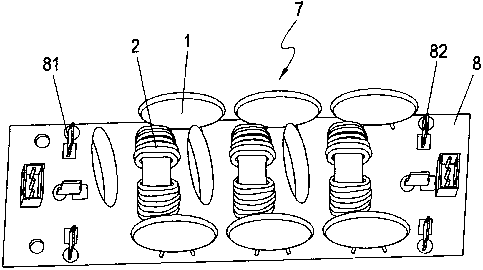
Please refer to FIGS. 1 to 7. A series surge suppression
structure mainly comprises:
a circuit board 8, a ground line 6 and a plurality of
galvanization circuits 4 being disposed thereon, a multilayer surge
absorption unit 7 being disposed in series on the ground line 6 and
the plurality of galvanization circuits 4;
wherein each surge absorption unit 7 is constituted by a pair
of chokes 2 with a layered surge absorption element 1 connected in
parallel between one end of either choke 2 and the ground line 6;
CA 02642314 2008-10-29
a power connection terminal 81, positioned on one side of the
circuit board 8 and electrically connected to a final end of the
multilayer surge absorption unit 7; and
a protection terminal 82, positioned on another side of the
5 circuit board 8 and electrically connected to a final end at another
side of the multilayer surge absorption unit7;
whereby, the protection terminal 82 can be used to connect with
a communication circuit 51 (as FIG. 7 shows) or an electric facility
52 (as FIG. 2 shows) and the power connection terminal 81 is used for
connecting with an external wire to allow the multilayer surge
absorption unit 7 on the circuit board 8 to be disposed in series
between the external wire and the communication circuit 51 or the
electric facility 52 to form the multiple surge absorption
protection.
Especially, according to the such kind of series surge
suppression method, the surge suppression elements 1(MOVs) and the
chocks 2 in the surge absorption unit 7 may constitute a multilayer
clamp voltage and tank circuit so as to be able to be used for
decreasing a remnant voltage and remnant energy to achieve the surge
substantially decreasing effect such that the facility can be
accurately effectively protected to prevent the damage of surge
invasion to enable a machine or a facility to maintain a normal
operation.
While being put into practice, as FIG. 2 shows, the number of
the galvanization circuits 4 is two, but it may be more than two
theoretically. Furthermore, the surge suppression elements 1 at
each layer assume a delta type disposition, but they may also assume
a Y-typed disposition.
Besides, as FIG. 1 shows, the surge suppression elements 1 and
the chokes 2 are distantly disposed on the circuit board 8 by means
of alternate permutation. Besides, only the chokes 2 may be disposed
on a middle part of the circuit board 8 by a distance and the surge
CA 02642314 2008-10-29
6
suppression elements 1 are respectively disposed on two sides of the
circuit board 8 by a distance as FIG. 3 shows. Otherwise, the surge
suppression elements are allowed to be disposed on a middle part of
the circuit board 8 by a distance and the chokes 2 are respectively
disposed on two sides of the circuit board 8 by a distance as FIG.
4 shows.
The structure of the present invention is very practical in fact
and has a very good effect to the surge suppression; it may be broadly
applied in various different electronic facilities or communication
facilities with a different working voltage (including AC and DC) and
a working current. Furthermore, it is more important that on an
entire planning design of the structure, a corresponding product may
be manufactured by calculating the following detailed formula while
the present invention is put into practice to provide the best surge
suppressing effect to different use requirements.
Please refer to FIG. 2 again. The circuit is constituted by
coupling the multiple sets of surge suppression elements 1(MOVs) to
the chokes 2 by means of a continuous series connection, in which the
plurality of surge suppression elements 1 are connected in parallel
by a distance by means of a multilayer type to relative connection
points 21 of the ground line 6 and the chokes 2 connected in series
with the plurality of galvanization circuits 4, and extended to L-N,
L-G and N-G to form a balance structure. In the figure, the surge
suppression elementsl at each layer assume a delta type disposition
(but they may assume a Y-typed disposition); it may then be applied
to an AC low voltage single phase facility by combining the layers
together to use as a protector for a general electric facility 52 or
a facility similar thereto.
Besides, as FIG. 5 shows, the circuit of the present invention
shown in FIG. 2 may be manufactured into a modular product by means
of a common standard specification so as to allow a user to select
and combine it with various different power specifications of
CA 02642314 2008-10-29
7
electric facilities. For example, the modular product may be used
for protection to an AC high voltage three-phase facility or put into
practice by coupling a power reactor to a lightning protector.
Please refer to FIG. 1, 2 and 5 again. FIG. 5 is a schematic
view of a derivative application of a modular product manufactured
from the circuit shown in FIG. 2. Each module 9 is constituted by
a circuit board 8 with a ground line 6 and a plurality of galvanization
circuits 4 disposed thereon and a multilayer surge absorption unit
7 is disposed on the ground line 6 and the plurality of galvanization
circuits. A power connection terminal 81 is disposed at one side of
each module 9, and a protection terminal 82 is disposed at another
side thereof; the power connection terminal 81 is also disposed on
one side of the circuit board 8 and electrically connected with a final
end of the multilayer surge absorption unit 7, and the protection
terminal 82 is also disposed on another side of the circuit board and
electrically connected with a final end of another side of the
multilayer surge absorption unit 7.
Please refer to FIG. 6. When the present invention is put into
practice, three (c5r multiple) modules are disposed in parallel, and
the protection terminals are disposed by connecting them together
with a delta type and then connected to an electric facility 52, and
the power connection terminals 81 are also disposed by connecting them
together with a delta type and then connected to an external wire.
Thereafter, the structure mentioned above can be used on three-phase
series-connection multilayer surge absorption protection. The
delta type is shown in the figure, but the aforementioned structure
may assume a Y-typed disposition.
The detailed description of how the present invention figures
out the surge suppressing effect accurately and a method for
manufacturing a product conforming to a practical demand depending
on a customer's requirement will further be given as the following.
For allowing a formula to be performed mathematical calculation
CA 02642314 2008-10-29
8
smoothly, any corresponding element notation will not be marked
during the following description. It is herby stated.
Besides, for conveniently giving an example to perform
mathematical calculations, the most basic circuit according to the
present invention shown in FIG. 7 is especially used for explanation.
The circuit is similarly constituted by coupling a plurality of surge
suppression elements (MOVs) to chokes 3 by means of continuous series
connection as the figure show, in which the same specification of
surge suppression element 1 (MOV) and the choke 2 may similarly be
adopted. The circuit may be applied for the protection on a
communication circuit 51 and facilities similar thereto.
Remnant voltage and remnant energy at two ends of a protected
facility in the figure may be represent by the following mathematic
expression.
A mathematic theoretical deduction of a method according to the
present invention bases on an assumption that the specifications of
the MOVs and the chokes used in each layer are the same. Approximate
50% of the surge current enters the MOVs and remnant 50% of the surge
current then enters the chokes.
Therefore, i=il'+i1=2i1, (i1'=i1) , il'=iZ+i2'=2i2, (Iz'=i2) ----
The surge current entering into the current shown in FIG. 7 is
i=i1 +il
in which corresponding points P1-P10 marked in the figure
respectively represent:
P1 represents a clamping voltage V,1 of a first layer, i1' is a
surge current flowing through the MOV.
P2, P3 respectively represent a voltage between two ends of the
choke of the first layer 2VL1 =2Llxdi1/dt.
P4 represents a clamping voltage Vc2 of a second layer, i2' iS
a surge current flowing through the MOV.
P5, P6 respectively represent a voltage between two ends of the
choke of the second layer 2VL2 =2L2xdi2/dt.
CA 02642314 2008-10-29
9
P7 represents a clamping voltage V,n of a nth layer, inis a surge
current flowing through the MOV.
P8, P9 respectively represent a voltage between two ends of the
choke of the nth layer 2VLn=2Lnxdin/dt.
P1O represents a remnant surge voltage between two ends of a
protected facility.
VC1=2VL1+ VC2
VC2=2VL2+ VC3
VCn=2VLn{' VCn+1
and
VL1 = (Lxdil/dt) = (1/2) 1 x (Lxdi/dt)
VL2 =(LXdi2/dt)=(1/2)2 x(Lxdi/dt)
VLn =(Lxdin/dt)=(1/2)n x(LXdi/dt)
Thus, a mathematic expression of the clamping voltage VC1 of the
MOV of the first layer is the following:
VC1 =2VL1 +2VL2 +-----+2VLn +VCn+l
VC1 =2 (VL1 +VL2 +-----+VLn) +VCn+l
VCn+l =VC1- 2 (VL1 +VL2 +----+VLn
Vcn+1 =VC1- 2 (LXdil/dt+LXdi2/dt+-----+LXdin/dt)
Vcn+1 =Vc1-2 [ (1/2) X (LXdi/dt+(1/2)2XLXdi/dt+--+(1/2)n XLxdi/dt) ]
VCn+l =VC1-2LXdi/dt[(1/2)+(1/2)2 +---+(1/2)n ]
VCn+l =VC1-2Lxdi/dt [2- (1/2 ) n ]
Thereby being able to obtain:
VCn+l = Vcl - [4- (1/2) n-1 ] (Lxdi/dt) formula (1)
When n=1, Vcn+1 =Vc1 -3 (LXdi/dt)^ when n=~, VCn+l =VC1 -4 (Lxdi/dt) .
The clamping voltage of the first layer VC1 and the clamping voltage
of the nth layer Vcn+1 ( i. e. the remnant surge voltage between the two
CA 02642314 2008-10-29
ends of the protect facility) are laid in between Vcl - 3(LXdi/dt)
and VC1-4 (Lxdi/dt) .
From the formula (1) we can know that inductance L and a surge
discharge current form a negative relationship. The remnant surge
5 voltage between the two ends of the protected facility lowers as the
surge current increases. Therefore, this method is able to suppress
the surge voltage more than a conventional method.
Energy Eabsorb absorbed when the surge current invade in FIG.7
can be expressed as the following mathematic expression according to
10 the method:
Eabsorb =
(il' )ZR +2(1/2)L(il)2 +(i2')ZR +2(l/2)L(i2)2 +---+(in' ) 2R +2(1/2)L(in)2
=R x[(ill )z +(i2' )2+---(in' )Z]+L[(11)Z +(i2)2 +----+(ln)2 ]
Because i=il'+i1 (i1'=i1) , i1'=iz+i2, (i2,=i2) , -----
E absorb =Rx[(i1,)Z +1/2(i11)2 +(1/2)2 (i1' ) 2 +---+(1/2)n(i1/)2 +
2X(1/2)L[(il)2 +1/2(il)2 +(1/2)2(il)2+---+(1/2) (il)2 ]
_ ( R+L ) [ (i l = ) 2 +1 /2 ( i l I ) 2+ ( 1 / 2 ) z ( i l l ) 2+---+ (112 )
n ( i lI ) 2 ]
=(R+L) [(il)2 +1/2(il )2 +(1/2)2(il )2 +---+(1/2) (il )z ]
=(R+L) (ill )z X[l+1/2+(1/2)2 +---+(1/2)n ]
The following result can finally be obtained:
Eabsorb =(R+L) (il)2 [2-(1/2)n ] formula(2)
When n=1, Eabsorb =1. 5(R+L) (il) Z ; when n=-, Eabsorb =2 (R+L) (ll) 2=
Energy absorbed when the surge invades is laid in between
1.5(R+L)(il)2 and 2(R+L)(il)2 according to the method of the present
invention.
Thus, the following result can be obtained:
Remnant energy of protected facility =
Total surge energy - absorbed invasion energy
Eremnant =Etotalsurge -Eabsorb formula ( 3 )
Because the surge suppressing effect generated from a series
surge suppression structure of the present invention can be derived
clearly from the aforementioned formulas (1) to know the remnant surge
CA 02642314 2008-10-29
11
voltage between the two ends of the protect facility, formulas (2)
and (3), remnant energy of a protected facility can be made clear so
as to be able to improve the deficits of a conventional method.
In addition, because FIG. 7 shows the most basic circuit
according to the present invention, FIG. 2 shows a derivative
application of the circuit shown in FIG. 7 in which a ground line is
added and FIGS. 5 and 6 respectively further show a broad derivative
application of the circuit shown in FIG. 2, the operational manners
and theories are all identical.
Therefore, the customization can be achieved through the reverse
application and deduction of the formulas (1), (2) and (3); how many
layers of chokes 2 and the value and specification of inductance L
of each choke need to be correspondingly used to manufacture a product
conforming to the practical demand can be known through a simple
conversion depending on a different power voltage (including AC and
DC) and load current requirement of electric facilities or
communication facilities.
Additional advantages and modifications will readily occur to
those skilled in the art. Therefore, the invention in its broader
aspects is not limited to the specific details and representative
embodiments shown and described herein. Accordingly, various
modifications may be made without departing from the spirit or scope
of the general inventive concept as defined by the appended claims
and their equivalents.
30