Note : Les descriptions sont présentées dans la langue officielle dans laquelle elles ont été soumises.
CA 02642645 2008-08-07
WO 2007/091119 PCT/IB2006/001533
ELECTROMAGNETIC RADIATION COLLECTION DEVICE
BACKGROUND OF THE INVENTION
Field of the llivention
[0001] The present invention relates generally to electromagnetic
radiation collection.
Related Art
[0002] The collection and concentration of electromagnetic (EM)
radiation is well lcnown. Radio waves are typically collected and concentrated
using parabolic dishes. Solar radiation is collected and concentrated using
parabolic mirrors or lenses. The former devices suffer fTom requiring a
relatively
high height-to-collection area ratio and the latter being expensive, heavy and
fragile. Both these types of device also suffer from the requirement to track
the
source in order to function properly.
BRIEF SUMMARY OF THE INVENTION
[0003] The invention seeks to overcome at least some of the
deficiencies in the prior art by providing an EM radiation collection device
which
can cover a large area, have a low profile, have no requirement to track the
source
and be constructed so as to be relatively light and inexpensive.
[0004] There is a pressing need to be able to generate energy from
renewable energy sources. Solar energy is one such resource which has
potential
to be exploited. Conventional devices for collecting radiant energy to
generate
energy in a useful form suffer from a high capital cost and/or the inability
to
generate high enough temperatures to be useful for inany applications. The
I
CONFIRMATION COPY
CA 02642645 2008-08-07
WO 2007/091119 PCT/IB2006/001533
invention seeks to overcome these deficiencies in the prior art by providing a
radiant energy concentration device that can gatller energy from a relatively
large
area and concentrate it onto a small target area. The device is relatively
inexpensive to produce, can be light in construction and has the potential to
generate high target temperatures or, in the case of conversion to electricity
by
photovoltaic cells, require only a small area of cells, thus saving cost.
[0005] The invention is directed to a device that can cover relatively
large collections areas at relatively low cost, does not necessarily require
materials
of particular refractive index and can be made of light construction.
[0006] The invention is capable of being less massive and having a
lower profile than prior art concentration devices. It is also capable of
having high
concentration factors. It is suitable in any application where it is desired
to collect
and concentrate EM radiation, with particular utility in the collection and
concentration of solar radiation. In the case of solar radiation, a device in
accordance with the inveiltion can be used in conjunction with photovoltaic
cells
or to heat a fluid to harness the solar energy for a desired puipose. In the
case of
radio frequency radiation, the subject device could be used to collect, focus
and
tune the radiation.
[0007] An exainple of a device in accordance with the invention is an
electromagnetic radiation collector that includes a chamzeling area having an
entry
end for receiving the electromagnetic radiation, an exit end, and at least one
reflective wall between the entry end and the exit end; and a radiation
collection
element near the exit end of the channeling area, the radiation collection
element
being adapted to collect the electromagnetic radiation.
2
CA 02642645 2008-08-07
WO 2007/091119 PCT/IB2006/001533
[0008] Another example of a device in accordance with the invention
is a control mechanism for a radiation collector where the radiation collector
is
adjustable to traclc a moving radiation source and where the control mechanism
comprises a first sensor to monitor the ambient radiation conditions and a
second
sensor to monitor the output of the radiation collector.
BRIFF DRSCRIPTION OF THE DRAWINGS
[0009] The foregoing and other features and advantages of the
invention will be apparent from the following, more particular description of
preferred embodiments of the invention, as illustrated in the accompanying
drawings wherein like reference numbers generally indicate identical,
fitnctionally
similar, and/or structurally similar elements.
[00010] Figure 1 shows an example of a channeling area;
[00011] Figure 2 shows an example of a device having multiple
channeling areas;
[00012] Figure 3 shows a cross-sectional view of an array of chailneling
areas;
[00013] Figure 4 shows a cross-sectional view of a different array of
channeling areas;
[00014] Figure 5 shows a first embodiment of the invention;
[00015] Figure 6 is a cut-away view of the embodiment shown in Figure
5;
[00016] Figure 7 shows a second embodiment of the invention;
3
CA 02642645 2008-08-07
WO 2007/091119 PCT/IB2006/001533
[00017] Figure 8 shows a side view of the einbodiment shown in Figure
7;
[00018] Figure 9 shows an alternate embodiinent related to the
embodiment shown in Figures 7 and 8;
[00019] Figure 10 shows a tliird embodiment of the invention;
[00020] Figure 11 shows an alternate embodiment related to the
embodinlent shown in Figure 10; and
[00021] Figure 12 shows a fourth embodiment of the invention.
DETAILED DESCRIPTION OF THE INVENTION
[00022] An exemplary embodiment of the invention is shown in the
drawings and described herein.
[00023] An example of a device in accordance with the invention has an
assembly of channeling areas wherein the EM radiation can be internally
reflected
within the cllanneling areas. In one embodiment, the channeling areas are
constructed such that at least some of the EM radiation that enters a broad
end of
the channeling areas will be steered within the cliaiuzeling areas to exit a
narrow
end of the channeling areas. The broad ends of the channeling areas are
assembled to folm a surface that is herein termed the collection surface. EM
radiation falls on the collection surface and enters the broad ends of the
charuleling
areas. The EM radiation is reflected from the walls of the chaiuleling areas
so as
to be directed to exit fioin the narrow end of the channeling areas. This is
achieved by ensuring that at each reflection point the angle of incidence of
the EM
4
CA 02642645 2008-08-07
WO 2007/091119 PCT/IB2006/001533
radiation to the reflecting surface is less than 90 . A method for ensuring
that this
is the case for a wide arc of angles of the EM radiation incident on the
collection
si.uface is to shape the chaiuleling areas such that they are much longer than
they
are broad at their broad end. This provides, in some einbodiments, a snlall
angle
of taper of the walls of the chaimeling area thus fillfilling the reflection
angle
requirements for a broader range of incident EM radiation angles. The ratio of
length of the channeling area to the breadth of its broad end should desirably
be
between 2 and 1000, more preferably between 5 and 100, and most preferably
between 10 and 50. Figure 1 shows an example of a single charmeling area and a
typical path 20 that EM radiation might take within the area.
[00024] The channeling areas can be made of solid material that is
capable of transmitting the EM radiation that is to be collected and
concentrated
and with walls that reflect the EM radiation back into the channeling area. In
another embodiment of the invention, the channeling areas are formed as
cavities,
where the walls of the cavities are capable of reflecting the EM radiation
back into
the cavity.
[00025] 1i1 one eznbodiment of the invention, the narrow ends of an
assembly of cham7eling areas are gathered together into an area that is
smaller than
the area of the broad ends of assembled chamzeling areas. In such an example,
the
EM radiation collected over the broad ends area is concentrated into the
narrow
ends area. An exainple of this einbodiment is shown in Figure 2.
[00026] In some embodiments of the invention, the channeling areas are
tapered in only one dimension, that is they take the form of tapered slots. In
otl7er
embodiments, the channeling areas are tapered in two dimensions so that they
take
5
CA 02642645 2008-08-07
WO 2007/091119 PCT/IB2006/001533
the form of tapered rods, where the rods can be of any cross-sectional shape
that is
suitable for packing together at high density. Examples of such shapes are
circles,
squares, rectangles, triangles and otlier znulti-sided polygons.
[00027] When the chaiuleling areas talce the form of tapered rods, to aid
in accommodating the curvature or the rods, maintain a high packing density
for
the broad ends of the chaiu-ieling areas and enhance the strength of an
assenibly of
the cllanneling areas, the channeling areas can be assembled suclz that each
channeling area is staggered relative to its neighbors. In a particular
embodiinent
of this aspect of the invention, rows of channeling areas are assembled such
that
the channeling areas in each row are offset from the row in front such that
the
narrow end of each channeling area is between the narrow ends of the
neigliboring
channeling areas in the rows immediately in front of and behind the subject
row.
By asseinbling the channeling areas in this way it is possible for the narrow
end of
each channeling area to curve into the space between the neighboring
channeling
areas in the row in front of it. This allows the channeling areas to be curved
while
maintaining high packing density of the broad ends of the channeling areas.
[00028] It is desirable to maintain a high packing density of the broad
ends of the channeling areas at the collecting surface so that the highest
fraction of
the EM radiation incident on the collecting surface enters a channeling area
and is
not reflected back.
[00029] hZ one embodiment of the invention, the chamzeling areas are
circular in cross-section and the broad ends are assembled in a packing
arrangement as is shown in Figure 3, where a top view of the asseinbled rows
of
the broad ends of the circular channeling areas are shown offset from one
another.
6
CA 02642645 2008-08-07
WO 2007/091119 PCT/IB2006/001533
Triangles are superilnposed on the view to show the relationship of the
centers of
the circular ends. This arrangement increases paclcing density and allows
space
for the chamieling areas to be curved as disclosed above. With this
ai7=angement, a
maximum fraction of 7r/2q3 (approx. 90%) of the incident radiation is
collected.
In a particular embodiment of this aspect of the invention, chamleling areas
witll a
square or rectangular cross-section are used. A top view of this arrangement
is
shown in Figure 4. With this shape of chamieling area, the broad ends of the
channeling areas can be packed such that close to 100% of the incident
radiation
enters the channeling areas and is thus collected. Note that in the embodiment
shown in Figure 4 it is possible, but not necessary, for the channeling areas
to be
of rectangular cross-section down their fi.ill length. For exainple, the
channeling
areas may be square or rectangular at the collecting surface but then
transition to a
circular area as we move down the chaiuleling area toward its tip.
[00030] Devices in accordance with the invention are usefi.il in
applications where EM radiation concentration devices have been used in the
prior
art, in particular solar radiation and radio frequency radiation. Examples of
such
uses particularly relevant to the collection and concentration of solar
radiation are
to heat fluid circulating through a tube or pipe, to generate electricity
directly
using photovoltaic cells or to produce hydrogen from water. Note that the
invention has particular utility in the application of producing electricity
using
photovoltaic cells as it allows the light to be collected from an extended
area using
the relatively inexpensive device of the invention and concentrate it on to a
relatively small area of the relatively expensive photovoltaic cells. This
potentially allows electricity to be generated at lower capital cost. Also,
this
7
CA 02642645 2008-08-07
WO 2007/091119 PCT/IB2006/001533
device addresses deficiencies in the conventional art when attempting to use a
concentrator with photovoltaic cells. Apart from expense and weight, the
conventional devices suffer from relatively low concentration factors of
typically
less than 10 and the problenl of the photovoltaic cells overheating and
becoming
less efficient.
[00031] A low profile collector and concentrator is desirable in
applications for radio fiequency (RF) radiation. In these applications, the
device
could be used to focus the RF radiation onto an RF receiver. Also, by careful
' choice of the dimensions of the channeling areas, the subject device could
be used
to tune the collected RF radiation to a frequency that can be received more
easily
by a receiver. For example, the device can be used to tune the RF radiation to
a
higher frequency, which requires a smaller and more easily implemented
receiver.
[00032] The subject devices can be made by any suitable method. The
channeling areas can be solid eleinents transmissive of light and made fiom
materials such as polymers or glass. For these solid elements, the walls of
the
elements can be coated with a reflective material or the refractive index of
the
material can be such tliat in most cases the incident angle of the EM to be
reflected
to the wall of the element exceeds the critical angle so that total internal
reflection
occurs. This embodiment has potential advantages in ease of fabrication but
can
also tend to be heavy. This embodiment could be constructed by manufacturing
many elements and assembling thein into arrays as disclosed above.
[00033] A particular einbodiment is one where the chaimeling areas are
cavities formed in a monolithic block made of metal or polymer material. This
may be soinewhat harder to fabricate but will be lighter. A method of
8
CA 02642645 2008-08-07
WO 2007/091119 PCT/IB2006/001533
manufacturing this einbodinient is to form an assembly of curved elements, for
example tapered elements, from a malleable material such as copper or nickel.
The assembly can be one of individual elements or of rows of elements formed
into combs where each tapered element is a"tooth" of the comb. Each comb
forins a row or portion of a row of the eleinents and the "teeth" of tlle
conibs of
successive rows in the assembly are staggered to give the arrangements shown
in
Figures 3 or 4. Before being assembled into an array, the elelnents can be
straight
or already curved. If the eleinents are straight, a bar can be passed over the
asseinbly of the narrow ends of the elements as a convenient method of
introducing the desired curvature. The assembled elements can be held in their
asseinbly by being clamped into a frame or other similar device. The curved
assembled elements, in conjunction with side walls and, if applicable, a top
and/or
base, can then be used as a mold for the final monolithic shape. The shape
with
the desired asseinbly of cavities can be molded by any applicable method. It
may
be cast by pouring polymer into the mold and letting it set of by injection
molding
techniques. In this process it is desirable to first coat the mold with a
suitable
release agent to facilitate removal of the mold elements from the cast shape.
After
the cast shape is set the mold elements can be removed. This can most easily
be
achieved by first removing the cast shape from the mold side walls, top and/or
base then unclamping the assembly of elements and removing them separately or
in groups as is nlost convenient and practical. Note that in most cases the
elements will need to be straightened somewhat to be withdrawn from the
cavities
so it is desirable that the material from which the tapered elements are made
be
malleable so that in can undergo the straightening process without breaking or
9
CA 02642645 2008-08-07
WO 2007/091119 PCT/IB2006/001533
distorting the shape of the cavity from which it is being withdrawn. This
process
results in a cast shape that contains an assembly of densely paclced curved,
light
guiding cavities, wherein the broad ends of the cavities all open onto one
face of
the shape and the narrow ends of the cavities all open on to a different face
of the
shape.
[00034] If the shape is not cast from an intrinsically reflective material
such as metal or metal filled polyiner, then the extei71a1 faces of the shape
and/or
the walls of the cavities can to be coated with a reflective layer. For
polyiner
material this is most easily achieved with an electroless metal deposition
process
sucll as electroless chrome or nickel deposition. A further transparent
coating
could be applied over the reflective coating if desired to protect the
reflective
coating.
[00035] An alteinative embodiment for creating an assembly of
channeling areas for collecting the EM radiation is to use a series of mirrors
that
focus the Iight into a series of spots or strips. In the case of a strip, the
optimal
mirror shape is parabolic in the plane of the strip and norinal to it. In the
case of
spots, the mirror is optimally a parabolic dish. According to this embodiment,
the
chaimeling areas are formed by the space between the adjacent mirrors where,
rather than the'adjacent mirrors fonning a tapering space, the tapering space
is
defined by the tapering shape of the radiation beain reflected from the rear
wall of
the chamiel. Also, the exit to the channel according to this embodiment is the
strip
or spot which is the focal point of the rear mirror. Therefore, in this
embodiinent
it is not necessary for the walls of the channel to taper in order for the
radiation
beam to be tapered. This has advantages in flexibility of design and in
minimizing
CA 02642645 2008-08-07
WO 2007/091119 PCT/IB2006/001533
the number of reflections that the radiation undergoes before exiting the
cliamlel.
The strips or spots that form the exit to the channel are arranged to be at
the focal
line or point of the nziiTor such that EM radiation reflected off the mirror
is
substantially concentrated onto them. To allow for different angles of EM
radiation incident on the mirrors, the mirrors can be rotated about their
focal line
or point such that the focus of the light remains co-incident witli the strips
or
spots. A control mechanism can perfonn the rotation whereby a signal, which
could be the output from an EM radiation target or from a separate sensor; is
monitored and the rotation of the mirrors performed so as to maximize the
amount
of EM radiation impacting the target. A particularly preferred embodiment of
sensor configuration is wllere the output of a separate sensor can be used in
combination with the output of the radiation target, or a sensor that
correlates to
the output of the radiation target, to achieve the control. According to this
embodinlent a separate sensor is configured to respond to the ainbient
conditions
with the target sensor output responding to the focusing configuration of the
mirrors. In the exainple of when PV cells form the target to generate
electricity
from solar radiation, a separate Iight sensitive sensor would be mounted away
from the mirrors such that it monitored the ambient incident radiation on to
the
panel. This sensor would for exaznple detect a change in the radiation level
due to
a cloud or other object passing between the sun and the panel. The target
sensor
on the other hand would monitor the output of the light impinging on to the
target
PV cells. So, the control mechanism would monitor both the ambient and the
target sensor and if the output of the two sensors varied in a similar way
over time,
then the control system would take no action as it would assume that the
change in
11
CA 02642645 2008-08-07
WO 2007/091119 PCT/IB2006/001533
output of the target was due to a change in the ambient conditions. If, on the
other
hand, the target sensor output changed in a different way to the ambient
sensor
otitput then the control systein would move appropriately to maximize the
output
of the target sensor.
[00036] The mirrors may have a rear reflecting surface that reflects EM
radiation onto one of the focusing mirrors.
[00037] An assembly of parabolic louvers that can be made to rotate
about tlieir focal line have been described above. The focal line of each
louver
impinges upon a receiving area in wliich one or more receiving elements are
placed. The receiving eleinents can be in the form of openings into a
concentration chamber, as disclosed in co-pending application
PCT/1B2005/003838, herein incorporated in its entirety by reference.
Alternatively, the receiving elements may be adapted to directly convert the
incident radiation. The receiving elements may be adapted to convert the
radiation
into electrical energy, for example photovoltaic cells could be placed in the
receiving areas. Alternatively the receiving elements maybe adapted to collect
the
thermal energy, thus transferring heat to a fluid medium whereby the energy
can
be utilized elsewhere. In the embodiment where PV cells are used as the
receiving
elements it is desirable to be able to cool the PV cells for their efficient
operation.
According to the cuiTent invention, cooling can be provided by having heat
dissipation areas between the areas of PV cells. Since these in-between areas
are
shaded from the incident EM radiation by the parabolic louvers they can
readily be
adapted to radiate heat efficiently, for exainple by coating them with a
radiating
coating such as a black coating. In an alteinative embodiment, a fluid layer
can be
12
CA 02642645 2008-08-07
WO 2007/091119 PCT/IB2006/001533
placed in a space below the plate containing the PVi cells and in thern-ial
contact
with the back of the PV cells. The fluid can be permanently contained within
the
space and allowed to circulate witllin the space, such that the fluid aids in
the
transfer of heat from tlle PV cells to the heat dissipation areas. In a fiu-
ther
embodiment the fluid can be allowed to, or made to, flow thougli the space
beneath the PV cells wlierein the heat is dissipated external to the plate
containing
the PV cells. Preferably, the PV cells could be connected in series to a
sufficient
extent to obtain the output voltage that is desired.
[00038] An advantage of particular embodiments of the present
invention is that there is space between the lines of PV cells. This allows
room for
the rows of cells to be connected in the desired fashion. For example each row
of
cells, or a portion of each row of cells under a particular focal line can
foim a
series element. An electrically conductive connection band can be placed in
the
spaces between each row of PV cells wherein the connection ba.ild extended
beneath one row of PV cells to effect electrical connection to the underside
of that
row of cells and a series of thin connection bands extended across the upper
surface of the second row of PV cells and otit to make connection with the
connection band between the two rows of PV cells. Alternative methods for
forming an electrical connection to the upper surface of the PV cells are
discussed
later in this disclosure. Preferably at least the lower connection bands would
be
nzade of material of high electrical and thermal conductivity, for example
copper
or aluminum.. The bands can be a single band made of one material or can be a
composite band made of one or more materials. For example, the portion of the
band that extends under the row of PV cells can be made of aluminum and the
13
CA 02642645 2008-08-07
WO 2007/091119 PCT/IB2006/001533
portion of the band between the rows of PV cells can be made of copper or
another suitable material. Preferably the bands of material can be deposited.
The
width of the band that is allowed by the space between the rows ofPVi cells
allows
a relatively thin film of coiulection band to have a relatively large surface
area and
cross-sectional area. The latter allows for low electrical resistive losses
and the
foriner allows for efficient heat dissipation of the heat generated by the EM
radiation impinging upon the PVi cells. The bands that extend across the top
of the
cells can be of any suitable material and in general would be of thin width so
as to
cover a minimum area of the PV cells.
[00039] In the case of the collection of tliermal energy, a conduit
containing a fluid to be heated could be placed at the focal line of each
parabolic
louver. Preferably this conduit is adapted such that it receives energy on one
surface from absorption of the concentrated EM radiation and its other
surfaces
are insulated to minimize heat loss. There could be multiple conduits or could
be
one or more conduits that extend to pass under two or more parabolic louver
focal
Iines. The con.duits would be made of thermally conductive material such as
copper. Since it is desired to have thermally insulating areas between the
conduits, unlilce the prior art, there is no need to have a plate such as a
copper
plate extend between the conduits. This reduces the cost and weight of the
device.
The theimally insulating areas can be filled with air or with insulating
materials
such as, for example, foams.
[00040] The profile of the reflective surface of the louvers is preferably
parabolic in shape. The profile of the parabola can be defined by the
equations
below. In these equations the focal point of EM radiation reflected from the
14
CA 02642645 2008-08-07
WO 2007/091119 PCT/IB2006/001533
parabolic profile is defined to be at the x, y point (0, 0). Also wliere xo
and yo are
defined to be the x and y coordinates respectively of the upper tip of the
parabolic
profile when the profile is rotated such that EM radiation nonnal to the x-
coordinate is focused on the focal point (0, 0). The profile is then defined
by the
equation:
[00041] y = tanao x2 _ xo
2xa 2 tan ao
ic ~
--atan ~o
2 xo
[00042] Where ao 2
= -
[00043] It is to be understood that due to manufacturing imperfection
and changes over time and temperature, the louver profile will only ever
approximately conform to the profile give by the equations above. The degree
of
conformance of the profile to the equation above will determine the width of
the
focal line that results in practice in the device. The louvers can be
manufactured
by any method that results in a reflective surface with a profile along its
length that
reflects an acceptable portion of the incident radiation on to a focal line of
the
desired width. An acceptable portion of the radiation is determined by
considerations of the overall cost of producing electrical or thermal energy
from a
specified area. This includes considerations of cost of manufacture of the
device,
its useful life, the efficiency of the energy conversion process and the
capabilities
of competitive tecluiologies. The desired width of the focal line is decided
upon
by a coinbination of factors balancing cost, practicality of manufacture,
device
longevity and ability to dissipate heat. These factors talcen together will
determine
the optimum width of the focal line for a particular lnanufacturing method and
CA 02642645 2008-08-07
WO 2007/091119 PCT/IB2006/001533
cost structure. For example, to reduce the cost of the PV cells, an expensive
component of the system, it is desirable to reduce their area, however, past a
certain point the cost of producing a reflector capable of the fineness of
focus
required and the ability to dissipate heat from the PV cells for their
efficient
operation becomes compromised, tlnis creating an optimurn width.
[00044] The louvers can be constructed of metal plates which are bent
to confornn to the desired profile. The plates can be intrinsically reflective
or
polished or coated and polished to forin a suitably reflective surface. These
metal
plates could be mounted in suitable motints to hold the plate at the rig11t
location
and to allow them to rotate about their focal lines. Alternatively, the
louvers can
be cast from metal, preferably with the motmting means integral, with the
reflective surface being polished or coated and polished after the casting. In
yet
another alternative, the louver, preferably with integral mounting means,
could be
cast or molded from plastic and subsequently metal plated to yield at least
the
front parabolic surface reflective. Optionally, the part could then be post
coated
with a clear layer to protect the reflective surface from environmental
degradation.
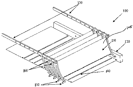
[00045] Figure 5 depicts one embodiment of the current invention.
Figure 5 depicts a partially assembled device 100 to ilhistrate the various
components. Reference number 110 denotes the front parabolic reflective
surface
of an exemplary louver 105. Pins 1501ocate the louver in side block 120 (only
one side shown) such that the focal line of the louver is coincident with the
target
area 140. Pins 1601ocate in tie rods 130 to link the louvers together. Pins
150
and 160 are free to rotate in the location holes in side blocks 120 and tie
rods 130,
such that when tie rods 130 are moved upward and forward in unison the louvers
16
CA 02642645 2008-08-07
WO 2007/091119 PCT/IB2006/001533
are rotated about the centre of the pins 150. Note that the centre of the pins
150
are coincident with the focal line of the corresponding louver such that the
louver
rotates about its focal line. This insures that for aiiy aiigle of incident
light in the
desired range the louvers can be rotated such that the focal line remains
coincident
with the target area 140.
[00046] Figure 6 depicts a fttrther cut-away illustration of the current
invention showing how incident radiation is reflected towards the target area.
The
aixows in Figure 6 show exeinplazy radiation paths. Note that the louvers are
spaced such that radiation that is not captured by one louver is captured by
the
louver in front of or behind it, thereby maximizing the collection efficiency.
[00047] Example 1: Louvers were designed with a parabolic reflector
shape according to equation (1) where xo and y,, were -37 min and 40 niin
respectively, with a louver pivot point separation of 22 rmn. End mounting
clamps
were constnicted with the computed shape by wire cutting the shapes out of
ahiminum. The mount clainps were made in two pieces with the concave parabolic
shape cut into the front of the rear half of the clamp and the corresponding
convex
parabolic shape formed as the rear surface of the front portion of the clamp.
0.2
mm thick brass sheet was nickel plated and polished to give a highly
reflective
surface and the plate cut into widths corresponding to that needed for a
louver.
The plated brass sheet was clainped at either end between the two halves of
the
mounting clamps. Steel pins were used to mount the mounting clamps to side
plates, where the pins were located in holes coincident with the focal liile
of the
louver. Pins in the upper end of the mounting clamps were mounted in holes in
a
17
CA 02642645 2008-08-07
WO 2007/091119 PCT/IB2006/001533
tie rod, as shown in Figure 5. Ten louvers witll a length of 200 mm were
assembled in this way.
[00048] Example 2: Louvers manufactured by injection molding were
fabricated. The parabolic shape was computed according to equation 1 with a:o
and
yo as -351nm and 60 mm respectively, with a louver separation of 20 mm and the
base of the louver being 7.15 mm above the focal plane of the louvers. The
dimensions were chosen such that the louvers could be rotated to be able to
accoinmodate incident radiation angles from 20 degrees to 115 degrees,
measured
from the x-coordinate, without the base of the louvers having to impact the
focal
plane. End mounts with integral pins were designed to be molded with the
louver
shape in one piece. The mold was constructed to give a mirror smooth finish on
the front parabolic surface. The louver was injection molded from an
ABS/polycarbonate blend Bayblend0 T 45 PG (Bayer MaterialScience) and then
metallized to form the reflective coating.
[00049] In one embodiment of the invention, narrow strips of PV cells
are placed at the focal lines to receive the concentrated radiation to convert
it to
electr-icity. To gather the current generated from the PV cells, it is
necessary to
make electronic connection to the upper and lower surface of the PV cells. It
is
also often desirable to connect a number of the strips of PV cells in series
to
generate a higher voltage axid decrease the current that needs to be carried
for a
particular power output.
[00050] According to the present invention, the lower connection to a
strip of PV cells is made by a conductive plate on which the PV cell sits. The
plate can be made from any material with sufficiently low electrical
resistance.
18
CA 02642645 2008-08-07
WO 2007/091119 PCT/IB2006/001533
Non-exclusive examples of suitable materials are aluminum, copper, tin aiid
copper covered with a layer of tin.
[00051] If it is desired that two or more PV cell strips are to be
connected in parallel then the lower connection plate is common to those
strips of
cells or individual plates are brought into electrical connection by other
means
such as by separate wires.
[00052] If it is desired that the strips of PV cells be coimected in series
then tllere is a separate lower comlection plate for each strip of PV cells.
The
cormection plate would extend beyond the edge of the strip of PV cells to
allow
otlier electrical comlections and to act as a heat dissipation device to cool
the PV
cells when in operation.
[00053] According to the present invention, the electrical cozlnection to
the upper surface of the PV cell strip is made by an electrically conductive
layer
placed in contact with the upper surface of the PV cell. In a preferred
embodiment, the upper surface connector is a continuous strip that runs the
length
of the PV cell strip, overlapping and in electrical contact with the upper
surface of
the PV cell strip along one lengthwise edge of the connector strip, in the
area of
the PV cell strip that is in shadow in operation. For the embodiment where the
PV
cells are to be comlected in series the otller lengthwise edge of the
connector strip
overlaps and is in electrical contact with the extension of the lower
corulection
plate of the next strip of PV cells. The connector strip in this elnbodiment
thus
makes a bridging electrical connection between the top surface of one strip of
PV
cells and the lower surface of the next strip of PV cells.
19
CA 02642645 2008-08-07
WO 2007/091119 PCT/IB2006/001533
[00054] Suitable materials for the upper connector strip are any
materials that can fornl a layer and have sufficiently low electrical
resistance.
Non-exclusive exainples of such materials are metals, metals coated with
electrically conductive adhesive, metals coated with a non-conductive
adliesive
but where the metal is textured such that areas of the metal peiietrate
through the
non-conductive adhesive, conductive inlcs, unsupported conductive adhesives
and
solder. Non-exclusive exaznples of suitable metals are aluminum, copper, tin,
tin
coated copper or silver. Non-exclusive examples of suitable conductive
adhesives
are pressure sensitive adhesives filled with silver or carbon such as
ARclad@9003 8 (Adhesives Research Inc, Glenn Rock, USA) and silver doped
epoxy. An exatnple of a suitable conductive tape with a conductive adhesive is
1181 Tape Copper Foil with Conductive Adllesive (3M Corporation). An
example of a suitable conductive tape coated with a non-conductive adhesive is
1245 Tape Embossed Copper Foil (3M Corporation) where the embossed features
on the foil penetrate through the non-conductive adhesive layer. Exainples of
suitable conductive inks are carbon or silver filled inks. Note that the upper
surface connector must only be capable of forming a continuous electron
conduction path from the PV cell to the next lower connector plate with
acceptably low electrical resistance. It need not be a continuous coiulection
path
along the length of the PV cell strip, as long as the overall resistance of
the
comiection of the upper surface of the PV cell with the lower coiulection
plate of
the next strip of PV cell is desirably low. For example, the connection could
be a
series of wires or dots bridging the gap to achieve the electrical connection.
However, a continuous connection layer down the length of the PV cell strip is
CA 02642645 2008-08-07
WO 2007/091119 PCT/IB2006/001533
usually preferred as in general it will lower the electrical resistance of the
coiuiection and will aid in heat transfer away from the PV cell to cool it for
more
efficient operation.
[00055] An additional advantage of the present invention is that there is
a small distance between any area of the upper surface of the PV cell exposed
to
the concentrated sunlight and the cuirent collector. The width of the PV cell
strip
exposed to the concentrated sunlight is small, at best equivalent to the width
of the
focal line from the parabolic louver minor. A typical widtli is less than 5 mm
and
more preferably less than or equal to 2 mm. So the current collected by the
upper
surface connector only has to travel a short distance through the PV cell
before
entering the low resistance connector. This reduces resistive losses in the
device
without the need to have any of the sunlight blocked from the PV cell by the
upper
surface connector.
[00056] Optionally, after the array of connections has been constructed
as illustrated above, part or all of the array could be overlaid with a layer
of
transparent material (as is known in the art) to protect the device from water
ingress, corrosion and mechanical damage. As a further option, the transparent
protective layer need not cover all of the array, but only cover the PV cells.
The
upper surface coiuzector and the lower surface connector could be covered with
a
layer to protect against corrosion and to aid the radiation of heat, for
example a
black paint or other thin polymer layer. Preferably there would be a good seal
between the transparent coating and the heat radiating coating to prevent the
ingress of moisture into the device.
21
CA 02642645 2008-08-07
WO 2007/091119 PCT/IB2006/001533
[00057] Figures 7 and 8 give a top view and cross-sectional view
respectively showing tlu=ee strips of PV cells comlected in series in one
embodiment of the present invention.
[00058] If it is desired to connect the strips of PVi cells in parallel then
the upper surface connector layer from one strip of PVi cells is coimected to
the
upper surface coimector layer of the next strip of PV cells. One embodiment of
the
connection method for parallel connection is shown in Figure 9.
[00059] In figures 7, 8 and 9, 210 denotes the lower surface connectors,
220 denotes the PV cell strips and 230 denotes the upper surface connectors.
In
operation, light is concentrated onto the areas pointed out by 220. In Figure
8, 240
denotes a support base which is electrically non-conductive or at least
electrically
insulated from 210 and 230. In Figure 9, 250 denotes side connection bars.
These
bars 250 serve to connect the strips of upper surface coimector together in
parallel
fashion. In this configuration the lower surface connector is a continuous
plate,
connecting the lower surfaces of the strips of PV cells in parallel fashion.
[00060] To connect an external circuit to the array of PV cells shown in
Figures 7 and 8, one connection would be made to the lower surface coiinector
210 at one end of the array and the other connection to 260, the plate
connected to
the upper surface of the last strip of PV cell. Optionally, the second
connection
could be made directly to the last upper surface connector in the array, in
which
case 260 is not necessary. To connect an external circuit to the parallel
array
shown in Figure 9, one connection would be made at any suitable location or
locations on 210 and the other connection at any suitable location or
locations o.n
one or both bars 250. The bars 250 are made of a material with low electrical
22
CA 02642645 2008-08-07
WO 2007/091119 PCT/IB2006/001533
resistivity. They could be made from the same material as the upper surface
connectors 230 or they could be made for example from copper wire or tirnzed
copper wire that is soldered to eacli upper surface comlector strip 230.
[00061] According to another embodiment, a solid electrically
conductive wire or ribbon is laid abutting one edge of the strip of PV
cell(s). The
wire or ribbon is of suitable cross-section such that it overlaps at least a
portion of
the adjacent conductive pad to which it is desired to connect the top surface
of the
PV cell(s). A bead of solder or conductive iidc can then be applied to form an
electrically conductive bridge between the top surface of the PV cell(s) and
the
conductive wire or ribbon. Optionally, an additional bead of solder or
conductive
inlc can be applied to form a conductive bridge between the conductive wire or
ribbon and the conductive pad. In the absence of this second bead, the fact
that
the conductive wire or ribbon overlaps and rests against the conductive pad
can be
used to provide sufficient electrical con.nection. A cross-sectional schematic
illustrating this aspect of the invention using a wire of substantially
circular cross-
section is given in Figure 10 and the situation wlien using a ribbon of
substantially
trapezoidal cross-section is given in Figure 11.
[00062] In Figures 10 and 11, the lower surface of the PV cell 320 is
placed in contact witll a conductive pad 310, which is forined on an
electrically
insulating substrate 340. A wire 330 (of circular cross-section in Figure 1
and of
trapezoidal cross-section in Figure 2) is placed so as to,abut one side of 320
and to
also overlap a portion of a second conductive pad 315. A bead of conductive
bridging material 350 increases the area of electrical connection between wire
330
and the top surface of the PV cell 320. A second, optional bead of conductive
23
CA 02642645 2008-08-07
WO 2007/091119 PCT/IB2006/001533
material 360 can be formed between 330 and 315 to increase the robustness of
the
comiection if necessary.
[00063] It is to be understood that this aspect is not restricted to any
particular cross-section of wire or ribbon but that any cross-section that
allows
bridging between the top surface of the PVi cell(s) and the adjacent
conductive pad
is witllin the scope of this invention. Examples of otller suitable cross-
sectional
shapes are, oval, triangular, square, rectangular, rhomboid, among otllers.
[00064] Suitable materials from which the wire or ribbon can be
constructed are any materials with suitably low electrical resistance through
the
cross-section of the wire or ribbon. Exainples of suitable materials are
copper,
ah.iminum, steel, stainless steel, brass and bronze.
[00065] The bead forming the bridge between the conductive wire or
ribbon and the top surface of the PV cells(s) can be made of any material and
applied by any method that is capable of laying down the bead within a pre-
defined area of the top surface of the PV cell(s) and bridging any gap between
the
edge of that surface and the adjacent edge of the wire or ribbon. For example,
a
bead of liquid solder can be applied. Alternatively, a length of solid solder
can be
laid against the wire and ribbon, such that it overlaps a pre-defined portion
of the
top surface of the PV cell(s) and the solder subsequently melted using heating
methods. In another example, a bead or layer of conductive iiilc can be
applied
from a dispensing device such as a nozzle or a printing screen, wllereupon the
ink
is dried or cured to fonn the finished bridge.
[00066] Another aspect disclosed here is to include reflective side walls
as part of the solar concentration module to improve light capture when the
24
CA 02642645 2008-08-07
WO 2007/091119 PCT/IB2006/001533
incident radiation is not norinal to the focal lines of the louvers. When
radiation
hits the parabolic iniiTor at an angle otlier tllan nonnal to its length, the
radiation
will be reflected at the same angle to the other side of the normal angle. In
otl-ier
words the reflected radiation will travel sideways as well as forward, when
loolcing from the front of the louver. Therefore, if nothing is done, a
portion of the
reflected light will not hit the receiving section on the focal line of the
mirror, but
rather travel past the end of the receiving section. There would also be a
commensurate portion of the receiving section at the other end of the louver
that
would receive no concentrated radiation. Therefore, in this situation, a
portion of
the radiation falling on the louver will not be focused on to a receiving
area.
[00067] According to this aspect of the current invention, this situation
can be avoided by installing additional reflective walls noimal to the focal
plane of
the parabolic mirrors and normal to the axis running along the length of the
parabolic inirrors. If this is done, the radiation that would otherwise be
lost is
reflected back and focused on to a portion of the receiving section for the
parabolic mirror.
[00068] This aspect of the invention is illustrated in Figure 12. Figure
12 depicts a cross-section view of the solar pane1400 when viewed from the
front.
The reflective side walls 410 and 420 and the focal plane 430 of the parabolic
miiTors (not shown) containing the receiving sections, are shown. The
radiation
440, is the reflected radiation from radiation incident on the leftmost
portion of the
parabolic louver. Radiation incident to the left of this radiation will be
blocked by
the side wall 410, creating a shadowed area 460. The radiation 450, is the
reflected radiation from radiation incident on the rightmost portion of the
CA 02642645 2008-08-07
WO 2007/091119 PCT/IB2006/001533
parabolic louver. The dotted lines depict the path of this radiation if the
sidewall
420 was not present. As is illustrated, the radiation 450 will be reflected
baclc on
to a portion of the radiation receiving area 470. Thus, this radiation will be
captured by the radiation receiver. Further, if the side wall 420 is normal to
the
focal plane 430 and noimal to the axis rumling along the length of the
parabolic
mirror, then the length of the ray reflected off 420 to reach the focal plane
and the
absolute angle of the light ray to 420 is the same as if the radiation were to
carry
on and be focused on the focal plane past the end of the receiving area
(depicted
by the dotted lines). Therefore, the radiation 450 reflected from the side
wall 420
will be focused onto a portion of the receiving section, and thus be correctly
captured. So, according to this aspect of the invention, although a shadowed
area
460 is created when radiation incident on the parabolic louver is not nonnal
to the
axis running long the lengtlz of the louver, a commensurate amount of extra
radiation is reflected by side wall 420 on to receiving area 470, resulting in
no net
loss of radiation. This allows the panel to efficiently concentrate radiation
from a
wide range of angles witliout the need to rotate the panel to face the source
of
radiation, for example the sun.
[00069] The side walls can be made of any suitable material with an
internal face that is reflective for the radiation that is beuig concentrated.
Examples are polished aluminum sheet, polished alumim.uil sheet covered with a
transparent coating, niclcel coated steel, bright clirolne coated steel,
nickel coated
brass or bronze, bright chrome coated brass or bronze, transparent plastic or
glass
coated on the baclc surface with a reflective coating and a baclc side
protective
layer applied, plastic with a front surface reflective coating with an
optional
26
CA 02642645 2008-08-07
WO 2007/091119 PCT/IB2006/001533
transparent over-coat to afford protection for the reflective coating or other
methods for creating a planar reflective surface.
[00070] It is to be appreciated that Figure 12 is merely illustrative and
that this aspect of the invention works equally well for radiation traveling
in from
the riglit side of 400, wllere 470 would become the shadowed area and 460 the
area receiving the extra radiation reflected off 410.
[00071] The invention is not limited to the above-described exemplary
embodiments. It will be apparent, based on this disclosure, to one of ordinary
slcill
in the art that many changes and modifications can be made to the invention
without departing from the spirit and scope thereof.
27