Note : Les descriptions sont présentées dans la langue officielle dans laquelle elles ont été soumises.
CA 02643923 2015-11-09
1
A High Power Laser Diode Array Comprising at least one High Power Diode Laser
and
Laser Light Source comprising the same
FIELD OF THE INVENTION
The present invention relates in general to high power diode lasers and
relates in particular to
a high power laser diode array comprising at least one high power diode laser
having multiple
emitters and more preferably comprising a plurality of high power diode lasers
having
multiple emitters, a method for manufacturing the same and an optical setup
for coupling the
output of such a high power laser diode array into an optical fibre.
BACKGROUND OF THE INVENTION
Most high power diode lasers are edge emitting semiconductors, with the laser
emitted from
one facet. Typical dimensions of one diode laser are a facet of 500 microns
wide and 100
microns high with a length between 0.6mm to 3mm. The optical brightness of the
diode laser
is defined by its internal structure. Parallel to the pn- junction (fast axis)
the emission is
diffraction limited and emerging from an aperture of about 1 micron with a
divergence of
typical 30 degrees (half angle for 11e2), in a direction parallel to the
mounting surface of the
diode laser the light is emerging from an aperture with a typical size in the
range of several
microns to 200micron and a typical divergence of 7 degrees (half angle for
1/e2).
High power diode lasers with output powers of 100W and more are realized by
arranging
multiple edge emitting diode lasers, so called single chips, next to each
other in one
semiconductor, so called array. In such cases, special measures have to be
taken to provide for
an efficient dissipation of heat generated by the multiple diode lasers.
Focusing the light of edge emitting diode lasers to a small spot requires
optical elements for
collimation and focusing. However, it is noted that the beam quality of such a
high power
laser diode is highly asymmetric. Typically, in fast axis the beam quality is
diffraction limited
CA 02643923 2015-11-09
2
in fast axis, characterized by M2=1 and in slow axis the beam quality for a
100 micron broad
aperture is in the range of M2=24. The issue of asymmetric beam quality in
fast and slow axis
is much more severe for high power arrays, with multiple single chips arranged
in one
semiconductor next to each other in slow axis direction. At a beam quality of
M2=1 in fast
axis, the beam quality in slow axis can decrease to M2=1.000. Because the
output laser beam
is highly asymmetric, typically two collimating steps are performed in the
prior art. Typically
first micro-optical lenses are used for collimating the highly divergent beam
in fast axis and
secondly, collimating lenses for slow axis collimation are deployed resulting
in a beam
collimated in both axis that can subsequently focused with one or more lenses
to a small spot.
Nevertheless, the symmetry of said collimated output laser beams is not
satisfactory for many
applications. Accordingly, there exists a need to provide simple and cost-
efficient solutions to
enable high power laser diodes to output laser beams of high beam quality, in
particular high
symmetry.
For coupling the light into optical fibers, which is a preferred application
of the subject-matter
of the present application, the beam quality must be symmetrized in fast and
slow axis.
Several concepts have been developed for beam shaping of diode laser arrays in
the past.
State of the art solutions use refractive or reflective optics to cut the
emission in slow axis in
several sections with subsequent rearranging in fast axis. Because of the high
divergence
angle in the fast axis direction, all these approaches dispose a collimating
lens for fast axis
collimation at very short distances from the emitting facet of the laser
diodes, i.e. make use of
collimating lenses of short focal length for fast axis collimation. This
approach usually
requires precise alignment of multiple micro-optical lenses in six axes, which
makes the
whole setup relatively complex and expensive. Nevertheless, a substantial loss
of beam
quality is experienced because of unavoidable tolerances in the parts, such as
smile of the lens
or diode array or the optical components for beam shaping, as well as in the
alignment of the
laser light emitter(s) to the associated optical component(s) and the optical
components
themselves.
Laser diode arrays of the above kind are disclosed e.g. by US 2003/0048819 Al,
US
2004/0114648 Al, US 5,715,264 and US 5,099,488.
CA 02643923 2015-11-09
3
In the following a high power laser diode, which forms the basis of the
subject-
matter of this application and is disclosed in EP 1 830 443 Al (published in
English
September 5, 2007) and US 2008/0084905 published April 10, 2008, will be
described
with reference to Fig. la to 3. As shown in Fig. la, the high power laser
diode
comprises a common heat sink 106 and a planar alignment substrate 110. The
laser diodes
102 are mounted on submounts 101 which are mounted onto the top surface of the
common
heat sink 106. As shown in Fig. lb, cut-outs formed by a central cut-out
portion 114, a left
cut-out portion 115 and a right cut-out portion 116 are formed in the
alignment substrate 110,
said cut-out portions being formed as through-holes in the alignment substrate
110. As shown
in Fig. la, the laser diodes 102 mounted onto the submounts 101 are fully
received by the cut-
outs 114-116 of the alignment substrate 110. As shown in Fig. lb, the
alignment substrate 110
comprises stops 119 formed as edges of the cut-outs 114-116. These stops 119
enable a
precise alignment of the laser diodes 101 and/or submounts 102 as will be
described in more
detail with reference to Fig. 4a to 5b below.
As shown in Fig. la, mirrors 107 are unitarily provided on the upper surface
of the heat sink
106 for deflecting the output laser beams by an angle of 90 degrees to a
direction of light
propagation designated by z' in the following (cf. Fig. 2a). The deflected
light beams pass
through the right cut-out 116 provided in the alignment substrate 110 near the
front facet of
the respective laser diode 102.
As shown in Fig. 2a, a planar spacer substrate 130 of a transparent material,
such as glass, is
bonded onto the top surface of the alignment substrate 110. Further, the fast
axis collimating
lenses 133, optionally made as an array, are bonded onto the top surface of
the spacer
substrate 130. For this purpose the fast axis collimating lenses 133 are
formed as piano-
convex lenses, the rear side of which being bonded onto the top surface 301 of
the spacer
substrate 130. The spacer substrate 130 is used for precisely defining the
distance between the
light emitting facets of the laser diode chips 102 and the downstream fast
axis collimating
lenses 133. Once a proper orientation and alignment of the lens array has been
found, this
orientation and alignment is fixed by bonding the lens array 133 to the spacer
substrate 130.
This high power laser diode as described above emits a plurality of fast axis
collimated output
laser beams, which propagate in the same direction (z') at equidistant
spacings between
neighbouring output laser beams and are aligned along a single line.
CA 02643923 2015-11-09
4
The set-up relies on highly accurate placement of the diode laser on the heat
sink in six axis,
which is practically very challenging. Based on an individual alignment of the
FAC lens, the
assembly tolerances for the diode laser can be significantly reduced for four
axis and by a
proper design of the beam size of the collimated beam.
Fig. 3a shows a setup for superposing two fast axis collimated output laser
beams of high
power laser diodes according to Fig. 2a and 2b each with an optical fill
factor of 50% and for
subsequent slow axis collimation as disclosed in EP 1 830 443 Al and US
2008/0084905.
Two high power laser diode modules configured as outlined above are arranged
perpendicular to each other. While the output laser beam of the module on the
left-hand side
passes the beam superposition prism 136 substantially unaffected, the output
laser beam of the
module on the right-hand side is reflected by the slanted surface of prism 136
such that the
two output laser beams are superposed with collinear optical axes. Downstream
of prism 136
there is provided a common collimating lens 137 for slow axis collimation to
generate a fast
- and slow axis collimated output laser beam 138. Thus, two rows of laser
diode emitters are
interleaved and the output laser beams superposed. For this purpose, a fill
rate of approx. 50%
is used to enable an output laser beam in the shape of a long line, but with
identical
divergences in slow and fast axis of the collimated beam. The superposition of
two output
laser beams as shown in Fig. 3a induces further optical losses through
inaccuracies of the
optical inteleaver and alignment tolerances of the individual rows.
US 6,771,686 B1 discloses a high power laser diode array comprising several
laser diode bars
with an associated fast axis collimator which is segmented in fast axis
direction and a slow
axis collimator. The planes of the diode laser bars are offset relative to
each other by half a
beam pitch. An optical element or a coupling element, which is located between
the slow axis
collimators and a focussing optics, the beams of the emitters are interleaved
with each other to
obtain a filling factor of 100%. This arrangement needs an optical interleaver
for interleaving
the output laser beams.
US 2005/0069260 Al discloses a setup for combining a plurality of laser beams
using
interleaved optical plates.
SUMMARY OF THE INVENTION
CA 02643923 2015-11-09
It is an object of the present invention to provide a simple arrangement of
diode lasers
wherein each output laser beam is individually collimated in fast and slow
axis by a set of
dedicated lenses or lens sections and wherein an output laser beam profile is
formed, without
the use of an optical interleaver, consisting of a plurality of fast and slow
axis collimated or
5 focussed output laser beams arranged adjacent to each other, i.e. next to
each other, in a
seamless manner in one dimension or in two dimensions with an optical fill
factor of 100% or
close to 100%. It is further a related object of the present invention to
arrange the diode lasers
such that all diode lasers are effectively coupled into optical fibers by
imaging all facets of the
diode lasers on the fiber end by means of reflective or refractive optics
only, avoiding any
beam shaping optics for rearranging the emission of diode lasers. It is a
further related object
of the present invention to further enhance the imaging and optical loss
characteristics of the
high power laser diode of the above configuration and at the same time to
enable a simple and
cost-efficient configuration for fast and slow axis collimation of the output
laser beams at less
tight tolerances. According to a further related aspect of the present
invention corresponding
methods for manufacturing such a high power laser diode are to be provided.
The above and further objects are achieved by the subject-matter as set forth
in the appended
claims.
A high power laser diode array according to the present invention comprises at
least one high
power laser diode comprising a plurality of laser light emitters for emitting
output laser beams,
each defining, in a direction perpendicular to a direction of propagation of
an output laser
beam, a fast axis and a slow axis; fast axis collimating means for collimating
said output laser
beams in fast axis direction to provide fast axis collimated output laser
beams; and slow axis
beam shaping means for collimating or focussing said output laser beams in
slow axis
direction, said slow axis beam shaping means being disposed external to said
at least one high
power laser diode; wherein said laser light emitters are displaced relative to
each other in fast
axis direction or in fast and slow axis direction by equidistant spacings,
respectively; and an
optical means is provided for foiming an output laser beam profile in the far
field of all laser
. 30 light emitters consisting of a said plurality of fast and slow axis
collimated or focussed output
laser beams arranged adjacent, i.e. next to each in a seamless manner in one
dimension or in
two dimensions with an optical fill factor of 100% or close to 100%. According
to the
invention the slow axis beam shaping means is comprised by or formed by said
optical means.
CA 02643923 2015-11-09
6
Thus, according to the invention the same optical means that serve(s) to image
the output
laser beams such as to arrange the fast and slow axis collimated output laser
beams adjacent
to each other in a seamless manner also serve(s) as the slow axis beam shaping
means for
collimating or focussing said output laser beams in slow axis direction.
According to the
present invention, the output laser beams which are emitted by the individual
laser light
emitters propagate already very close to each other, due to the particular
arrangement of the
high power laser diodes as set forth below. This means, that only very narrow
gaps exist
between the output laser beams which are emitted by the individual laser light
emitters or that
the overall beam profile of the high power laser diode array even consists of
said plurality of
fast and slow axis collimated or focussed output laser beams arranged
adjacent, i.e. next to
each in a seamless manner in one dimension or in two dimensions with an
optical fill factor of
100% or close to 100%. Thus, the optical means does not rearrange the
individual output laser
beams, as in the prior art, but only reduces the gap between adjacent output
laser beams, if
this should exist, to substantially zero to achieve the fill factor of 100%.
According to some
embodiments of the present invention, the optical means also focuses or
collimates the fast
axis collimated output laser beams in slow axis direction. According to other
embodiments,
however, a slow axis collimating means might also be disposed downstream of
the optical
means.
According to an embodiment the laser light emitters are displaced relative to
each other in a
chessboard-like manner so that in combination with a suitable optical means,
such as an array
of parabolic hollow mirrors or refractive optical lenses, the output laser
beams are arranged
next to each other in a seamless manner in one or two dimensions, i.e. such
that neighbouring
output laser beams are substantially adjacent to each other, without a
significant gap of low or
vanishing light intensity therebetween. In this manner an optical fill factor
of the output laser
beam profile of 100% or close to 100% is achieved. More specifically the
output laser beam
profile preferably consists of a plurality of output laser beams that are
collimated or focussed
in fast axis direction and collimated or focussed in slow axis direction and
arranged in a
chessboard-like manner. Output laser beams of neighbouring rows may be
displaced by half a
beam pitch which enables to efficiently generate output laser beam profiles of
arbitrary shape,
such as circular, elliptical, line-shaped, rectangular, etc. beam profiles.
According to an embodiment the laser light emitters of each high power laser
diode are
disposed at equidistant spacings relative to each other in fast axis
direction, preferably along a
CA 02643923 2015-11-09
7
single row. Furthermore, neighbouring high power laser diodes are offset
relative to each
other, at equidistant spacings, in slow axis direction. In this manner, the
above chess-board
like arrangement of the output laser beams is achieved without the use of
additional
interleaving means that, according to the prior art, are used to rearrange or
at least deflect the
output laser beams.
According to an embodiment the fast axis collimating means is or are
integrated into a
respective high power laser diode, using a planar substrate means which
receives or supports
the fast axis collimating optical element, such as a refractive lens, a
diffractive optical element
or a reflective mirror. Thus, a stable and precise fast axis collimation is
accomplished.
According to another preferred embodiment each of said slow axis beam shaping
means is a
reflective parabolic hollow mirror of a shape suited for collimating or
focussing an associated
output laser beam in slow axis direction. Thus, the high power laser diode
array provides a
plurality of output laser beams that are collimated both in fast and slow
axis.
According to another preferred embodiment several or all of said parabolic
hollow mirrors are
formed in a common substrate by micro-machining or diamond-machining of said
substrate,
preferably a copper body, or by press-forming of a glass, which enables an
efficient mounting
and cooling of the slow axis collimating means.
According to another embodiment, the common substrate is actively cooled,
preferably by a
fluid flowing through the common substrate, to avoid excessive heating of the
common
substrate due to reflective and/or absorptive losses caused by said parabolic
hollow mirrors.
According to another preferred embodiment, the slow axis beam shaping means is
or are
configured for collimating said output laser beams in slow axis direction,
such that said high
power laser diode array provides fast and slow axis collimated output laser
beams of a
predetermined width in fast axis direction and slow axis direction,
respectively, wherein said
laser light emitters are displaced relative to each other in fast axis
direction and/or slow axis
direction by a fraction 1/n of said predetermined width in fast axis direction
and/or of said
predetermined width in slow axis direction (n being an integer larger than or
equal to 1,
preferably equal to 2) and wherein said fast and slow axis collimated output
laser beams are
interleaved in a seamless, chessboard-like manner.
CA 02643923 2015-11-09
8
According to another embodiment, the laser light emitters are aligned along at
least two rows,
at equidistant spacings between two neighbouring laser light emitters of a
respective row,
wherein neighbouring rows of high power laser diodes are alternately shifted
in fast axis
direction by a fraction 1/n of said spacing (n being an integer larger than or
equal to 1,
preferably equal to 2). This optical arrangement enables an efficient
interleaving of output
laser beams in order to obtain an output laser beam profile consisting of a
plurality of output
laser beams interleaved in a chessboard-like, seamless manner.
According to another embodiment each of said high power laser diodes emits a
plurality of
fast and slow axis collimated output laser beams spaced apart from each other,
the output fast
and slow axis collimated laser beams of two neighbouring rows of high power
laser diodes
intermeshing in a comb-like manner.
- 15 BRIEF DESCRIPTION OF THE DRAWINGS
Hereinafter, the invention will be set forth in exemplary manner and with
reference to the
accompanying drawings, from which further features, advantages and problems to
be solved
by the present invention become apparent to a person skilled in the art and
wherein:
Fig. la and lb show the mounting of an alignment substrate and the laser diode
submounts on
a heat sink of an embodiment according to the prior art in a side view and a
top
view;
Fig. 2a and 2b show the embodiment according to Fig la and lb with fast axis
collimating
lenses mounted on the top surface of the spacer substrate in a side view and a
top
view together with output laser beams; (why take the figure with 100% optical
fill
factor, Fig. 3a becomes less clear that way);
Fig. 3a shows the superposition of two laser beams output by two single
laser diodes
according to the prior art of a configuration as described with reference to
fig. 2a
to 2b;
Fig. 4a and 4b shows the alignment substrate for mounting the laser diode
submounts on a
common heat sink according to an embodiment of the present invention in a side
view and a top view;
CA 02643923 2015-11-09
9
Fig. 5a and 5b show the embodiment according to Fig. 4a and 4b with fast axis
collimating
lenses supported in a planar substrate in a side view and a top view together
with
output laser beams;
Fig. 5c shows the embodiment according to Fig. 4a and 4b in a top view
onto the end face
of the high power laser diode and along the direction of alignment of the
laser
diodes of this high power laser diode;
Fig. 5d shows a modification of the embodiment shown in Fig. Sc having a
unitary planar
substrate for supporting the fast axis light collimating lenses;
Fig. 5e shows a modification of the embodiment shown in Fig. 5c having a
planar
substrate consisting of a lower and upper planar substrate;
Fig. 5f shows a modification of the embodiment shown in Fig. Sc, wherein
the fast axis
collimating lens is tilted in order to obtain a lateral beam shift for
adjusting the
position of an associated output light beam collimated in fast axis direction;
Fig. 5g shows in a perspective top view the common heat sink with
integrated beam
bending mirrors of a high power laser diode according to the present invention
with a plurality of light emitters disposed on an upper surface thereof and
aligned
along a single row or line;
Fig. 5h shows the high power laser diode according to Fig. 5g with a
planar substrate
mounted on a surface of the common heat sink for holding a plurality of
cylindrical, aspheric lenses for fast axis collimation;
Fig. 6a shows a high power laser diode array according to a first
embodiment of the
present invention for slow axis collimation of three linear high power laser
diodes
disposed in parallel with each other under a predetermined pitch in two axes;
Fig. 6b shows the beam profile obtained using the first embodiment shown
in Fig. 6a;
Fig. 6c shows a high power laser diode array according to a second
embodiment of the
present invention for slow axis collimation of three linear high power laser
diodes
disposed in parallel with each other under a predetermined pitch in only one
axis;
Fig. 6d shows a high power laser diode array according to a third
embodiment of the
present invention for slow axis collimation of three linear high power laser
diodes
disposed in parallel with each other under a predetei mined pitch in one
axis;
Fig. 6e shows the beam profile obtained using the third embodiment shown
in Fig. 6d;
Fig. 6f shows a top view of the high power laser diodes of the first
embodiment shown in
Fig. 6a together with the slow axis collimators integrated into a common heat
sink;
CA 02643923 2015-11-09
Fig. 6g shows a perspective view of the optical setup shown in Fig. 6f;
Fig. 6h shows the slow axis collimator array used with the optical setup
shown in Fig. 6g;
Fig. 6i shows a laser light source according to the present invention,
wherein the output
laser beam of a high power laser diode array according to the present
invention is
5 focused onto the entrance facet of an optical fibre;
Fig. 7 shows another embodiment of the present invention wherein the
laser light
emitters are each disposed individually on a step-like substrate with
monolithic
slow axis beam shaping means on an opposite side; and
Fig. 8 shows a modification of the high power laser diode array shown in
Fig. 6a,
10 wherein the hollow mirrors are focussing the output laser beams both
in slow and
fast axis.
Throughout the drawings like reference numerals relate to identical or
substantially equivalent
elements (components) or groups of elements (components).
DETAILED DESCRIPTION OF PREFERRED EMBODIMENTS OF THE PRESENT
INVENTION
With reference to Fig. 4a to 5c the configuration of a high power diode laser
for use in a high
power laser diode array according to the present invention and the most
important steps for
manufacturing such a high power diode laser will be described in more detail.
As shown in Fig. 4a and 4b, the diode laser chip 2 is mounted on the top
surface of a
submount 1, which is of a substantially rectangular shape having straight
edges perpendicular
to each other. The submount 1 can be made of any material suitable for
supporting a laser
diode chip. Preferably the submount is of a high heat conductivity material in
order to spread
heat generated by the diode laser chip 2 to a carrier 6 supporting the
submount 1. Furthermore,
the material of the submount 1 preferably has the same coefficient of thermal
expansion as the
semiconductor material of the diode laser chip. Suitable materials for the
submount 1 that
shall not be deemed limiting the present invention are: AIN, CuWo or diamond.
Typical
dimensions of a submount I for use according to the present invention are 4mm
by 4mm.
On the surface of the submount 1 there are provided in a conventional manner
bond pads for
contacting the diode laser chip 2. More specifically, a bond pad 3 for
contacting the n-doped
CA 02643923 2015-11-09
11
layer of the diode laser chip 2 and a bond pad 4 for contacting the p-doped
layer of the diode
laser chip 2 are provided. If the submount I is conductive, the above p-bond
pad is not
provided. Bonding wires 5 extend across the gap between the pad 3 and laser
diode chip 2 for
supplying electric power to the diode laser chip 2. As will be apparent to a
person skilled in
the art, both the pads 3, 4 and the diode laser chip 2 slightly protrude from
the top surface of
the submount I.
As shown in Fig. 4a, the diode laser chip 2 defines a fast axis (y)
perpendicular to the
direction of propagation (z) of the uncollimated output laser beam 30 and a
slow axis (x)
perpendicular to the fast axis and direction of beam propagation. The fast
axis y is parallel to
a plane defined by the pn-junction of the diode laser chip 2. As shown in Fig.
4b, the diode
laser chip 2 is mounted in a well-defined orientation on the top surface of
the submount 1.
More specifically, the front facet of the diode laser chip 2 is substantially
flush and parallel
with the front edge of the submount 1 and the longitudinal side surface of the
diode laser chip
2 is substantially in parallel with an edge of the submount 1. As an
alternative, the front facet
can also protrude slightly from the front edge of submount 1 or can be
disposed at a short
distance, and in parallel with, the front edge of submount 1. In order to
enable such an
alignment of the diode laser chip 2 with regard to edges of the submount 1,
stops such as
those set forth below may be provided on a surface of the submount 1 so that a
proper
alignment of the diode laser chip 2 is obtained by abutment of one or more
edges of the diode
laser chip with an associated stop. Accordingly, in the embodiment according
to Fig. 4a and
4b, the output laser beam 30 is emitted in z-direction which is substantially
perpendicular to a
front edge of the submount I and substantially in parallel with the top
surface of the submount
1. As will become apparent to a person skilled in the art, the diode laser
chip 2 can also be
mounted in any other suitable orientation on submount 2. As will become
apparent to a person
skilled in the art, the active layers of all diode laser chips lie in a common
plane.
As shown in Fig. 4a a planar, i.e. piano-parallel, spacer substrate 10 is
mounted on the top
surface of the common heat sink 6. As will be shown below in more detail,
according to the
present invention the spacer 10 serves to support or receive the fast axis
collimating lenses.
used for fast axis collimation of the output laser beams of the diode laser
chips in a precise
orientation and position in order to obtain a desired fast axis collimation.
Based on an
individual alignment of the FAC lens, the assembly tolerances for the diode
laser are
significantly reduced in all three translational axis to tenths of micrometer
and for one
CA 02643923 2015-11-09
12
rotational axis (around slow axis vector) to degrees. As set forth below in
more detail, the fast
axis collimating lenses are integrated into the high power laser diodes.
The spacer 10 generally is of rectangular shape and has a plurality of cut-
outs 14 and 16 in
accordance with the total number of laser diode submounts to be mounted.
According to Fig.
4b the cut-outs 14 and 16 form a substantially rectangular window. As will be
explained in
more detail with reference to Fig. 5a and 5b, the cut-out 16 serves as a
window for passing the
output laser beam through the spacer substrate and toward downstream fast axis
collimating
lens, whereas the cut-out 14 serves for accessing the diode laser 2 mounted to
a submount 1
and the wire bonds 5 with the respective bond pads 3, 4 (cf. Fig. 4b). Cut-
outs 14 and 16 can
be of the same width allowing only partial access to the diode laser mounted
and bonded to
the submount. Furthermore cut-out 16 may comprise a lower recess 11 that is
formed such
that the fast axis collimating lens rests on the upper surface of the lower
recess 11 and is
roughly held in position by the sidewalls 22 of the cut-out 16. As will become
apparent to a
person skilled in the art a cut-out of any other suitable shape may be
provided in order to
enable alignment of the laser diode chips and/or submounts.
As described in more detail in EP 1 830 443 Al and US 2008/0084905, a
precision
tooling or the substrate 10 can be used for precisely positioning the laser
submounts and/or
laser diode chips in the following manner: the central cut-out 14 is limited
by a central
rectangular protrusion protruding from a right longitudinal web of substrate
10. The top of
protrusion serves as an alignment stop for the diode laser chip, as will be
explained in more
detail below. A small step portion can be provided at the right-hand side of
protrusion to
thereby form a second alignment stop, perpendicular to alignment stop, as will
be explained in
more detail below. The height of step portion in transverse direction is
smaller than the width
of the laser diode chip 2 in slow axis direction, e.g. corresponds to approx.
10% - 30% of the
total width of the laser diode chip 2 in slow axis direction. Furthermore, the
thickness of the
substrate 10 can be substantially larger than the height of the laser diode
chip in a direction
perpendicular to the plane of the pn-junction. Preferably the thickness of the
substrate 10 is
substantially larger than the height of the bond pads 3, 4 (cf. Fig. 4b) on
the top surface of
submount 1. Thus, it can be ensured that both the laser diode chip 2 and the
bond pads 3, 4
together with the bonding wires 5 are substantially fully received by the cut-
outs 14, 16
CA 02643923 2015-11-09
13
formed in the lower surface of spacer and alignment substrate 10, when the
submounts are
mounted to the spacer and alignment substrate 10.
As will become apparent to a person skilled in the art, the spacer can be made
of any material
suitable to allow precise formation of straight alignment stops having a
predetermined
orientation. According to a preferred embodiment of the present invention, the
spacer will be
made of a material identical to that of the heatsink 6 to minimize thermo-
mechanical stress
and deformation, in particular of copper, in which case the cut-outs and
alignment stops can
be formed easily and precisely using conventional machining techniques.
However, the
invention is not limited to use of copper as basic material for the spacer.
Other suitable
materials not limiting the present invention are glass and ceramics. Some of
these materials
are suited as well for machining techniques for forming the cut-outs and/or
alignment stops
with high precision and orientation. As will become apparent to a person
skilled in the art, the
cut-outs and/or alignment stops can also be produced even at sub-micron
precision using
other processing techniques, such as laser cutting, micro-machining and the
like. It is noted
that there is no need for the spacer and alignment substrate to be optically
transparent to the
output laser light.
Fig. 4a and 4b show how according to the first embodiment of the present
invention the laser
diode submounts 1 are mounted to the heatsink 6. As shown in Fig. 4a and 4b,
the submount 1,
the bond pads 3, 4 and the laser diode chip I are received in the cut-out 14
formed in the
spacer 10. Due to the afore-mentioned stops the longitudinal side surface of
laser diode chip 2
is substantially parallel to the alignment stop on protrusion or abuts the
alignment stop for
precisely adjusting the angular orientation of the laser diode chip 2 with
respect to substrate
10 in slow axis direction x. Furthermore, according to Fig. 4b, the edge
emitting facet of laser
diode chip 2 is substantially in parallel with the alignment stop of the step
portion used for
precisely adjusting both the longitudinal position of laser diode chip 2 with
respect to
substrate 10 and the angular orientation of the laser diode chip 2 with
respect to substrate 10
(y-direction; cf. Fig. 4a). It is noted that the submount 1 can also contact
the left longitudinal
web. As shown in Fig. 4b, a portion of the left edge of submount 1 does not
contact the left
longitudinal web 11 of substrate 10 so as to prevent build-up of tensions in
submount 1. As
shown in Fig. 4a, the bond pads 3, the laser diode chips 2 and the bonding
wires 5 are fully
received by the cut-outs fonned in spacer 10 when the spacer 10 is mounted to
heatsink 6.
According to another embodiment the laser diode chips are aligned to the
submounts as
CA 02643923 2015-11-09
14
described above. Alignment features provided on the submount and/or on the
planar spacer
substrate and/or planar alignment substrate enable a corresponding precise
alignment as will
become apparent to a person skilled in the art.
As shown in Fig. 4a, reflective mirrors 7 are disposed on the upper surface of
the heat sink 6
for deflecting the output laser beams upwards by an angle of ninety degrees,
i.e. perpendicular
to the top surface of the heat sink 6. The mirrors 7 are slanted by 45 degrees
with respect the
upper surface of heat sink 6. Such slanted portions can be manufactured e.g.
by diamond-
machining the surface of the mirror 7 and may be coated by a reflective
coating e.g. with gold.
Preferably, the mirrors 7 are plane mirrors. However, according to alternative
embodiments,
the mirrors 7 can also have a surface profile for shaping the beam profile of
the output laser
beams, e.g. the mirrors 7 may be fowled as concave or convex hollow mirrors.
In operation the uncollimated output laser beams 30 are deflected by the
mirrors 7 from a
direction of propagation z by 90 degrees to a direction of propagation z' to
thereby pass the -
cut-out portions 16 of spacer 10 (cf. Fig. 4b). Although not explicitly shown
in the schematic
drawing according to Fig. 4a, the thickness of the spacer 10 in the direction
of propagation z'
is substantially larger than the lateral dimensions of the laser diode chips
2. According to the
present invention, the thickness of the spacer and alignment plate 30 is of
the order of
millimetres (mm), a suitable thickness lying in the range between lmm and 5mm
and more
preferably in the range between 2mm and 4rnm. Thus, the light cones in the
fast axis direction
y, y' of the uncollimated output laser beams 30 have opened substantially when
reaching the
entrance window of the fast axis collimating lenses, which will be described
below.
The cut-outs 14 and 16 described above with reference to Fig. 4b extend
through the entire
height (in z' direction) of the spacer 10 but recesses may be foimed in cut-
out 16 in the upper
surface of the substrate 10, as can be concluded from Fig. 5a. The width of
cut-out 14 and 16
may also be of the same width. As shown in the top view of Fig. 4b, in the
plane of the
substrate 10 this recess is limited by perpendicular sidewalls defining an
inner perimeter 11 /
22 of the substrate 10. More specifically, the inner perimeter 22 defines a
region of reduced
width so that the uncollimated output beam of the laser diode chips can
propagate to the
recess unhindered, while the fast axis collimating lens inserted in cut-out 16
may rest on
protrusion defining a specific distance to the diode laser and being fixed to
either the recess or
the sidewalls 22 of cut-out 16.
CA 02643923 2015-11-09
The central cut-out 14 may also not extend through the entire thickness of
spacer 10 in order
to further improve the thermal management and heat dissipation, but may be cut
through to
enable an unhindered access from above to underneath components, such as the
submounts 1
5 and/or laser diode chips 2 during assembly, e.g. for mounting and/or
adjusting the position of
these components.
As shown in Fig. 4b the two opposing sidewalls 22 of cut-out 16 may form a
rectangular
bottom surface that protrudes from the perimeter formed by cut-out 16. As will
be shown
10 below these rectangular bottom surfaces may serve to support the planar
backsides of fast-
axis collimating lenses.
As shown in Fig. 5a fast-axis collimating lenses 32 may be supported by the
rectangular
bottom surface of the recess formed by the two opposing inward protrusions 22.
The fast-axis
15 -collimating lenses are individual aspheric lenses 32 in this example but
can be formed,
according to related embodiments, as a lens array having a planar backside.
The fast-axis
collimating lenses 32 may be supported only at side edges thereof on the
rectangular bottom
surface of the recess or at the two opposing sidewalls 22, whereas the output
laser beams pass
the lenses 32 only in the central region thereof Therefore the beam profile
and homogeneity
of the output laser beam is not affected by bonding the lenses 32 either at
the bottom surface
of the recess or at the sidewalls 22 to the spacer 10.
As an alternative to what has been described above with reference to Fig. 4a
and 4b the
substrate 10 may also be used only for supporting the fast axis light
collimating lenses 32 in
an appropriate manner, i.e. not for precisely positioning the laser diode
submounts and/or
laser diode chips themselves. According to such a preferred embodiment of the
present
invention, the laser diode submounts and/or laser diode chips are exactly
positioned onto the
top surface of the common heat sink 6 using a positioning device such as a
template or screen
for exactly positioning the laser diode submounts and/or the laser diode
chips. Afterwards the
laser diode submounts and/or laser diode chips are bonded or soldered onto the
common heat
sink in a single refiow process or the like while being positioned by the
positioning device.
Individual alignment and soldering of each chip is also possible. After
removal of the
positioning device the planar substrate 10 is mounted onto the common heat
sink 6, which
does not require a very precise positioning thereof Afterwards the fast axis
light collimating
CA 02643923 2015-11-09
16
lenses 32 are mounted on the planar substrate. For this purpose a single
rectangular recess
suited for at least partially receiving all fast axis collimating lenses 32 or
a plurality of
recesses each suited for at least partially receiving a single fast axis
collimating lens 32 is/are
formed in the upper surface of the substrate 10. As an alternative the
recess(es) may be
formed as a through hole of appropriate shape in the substrate 10.
For mounting the fast axis collimating lenses 32 to the substrate 10, the
lenses 32 are inserted
from above into the cut-out 16 with optional recesses and then adjusted to
ensure a proper
beam quality. Displacements of the diode laser in the directions of the fast
axis and optical
axis are corrected for each diode laser individually through precise alignment
in 5 axis to the
respective diode laser. Angular misalignment around the slow axis vector are
corrected by a
respective shift of the fast axis lens in the plane parallel to the mounting
surface of submount
2. Translational misalignment of the diode laser in slow axis is corrected by
tilting the fast
axis lens 32 around the rotated fast axis direction. The fast axis lenses are
aligned such that
the beams 34 of one high power diode laser are all collimated in fast axis
direction with their
main axis 31 being all parallel to each other in fast and slow axis direction.
Thus the substrate 10 serves to support the fast axis lenses such that they
are precisely
adjusted for (a) equal distance between the light emitting facets of the laser
diode chips and
the entrance window of the fast axis collimating lenses 32 and (b) equal
orientation of
radiation emitted from all diode lasers. The substrate 10 is designed such
that additional
optical elements, such as a low reflective window may be attached to the
substrate e.g. to seal
the fast axis collimated diode laser against ambient conditions.
The fast axis collimating lenses 32 are made e.g. by press-forming or micro-
machining a
transparent glass substrate or resin or any other suitable method. They can
also be diamond
machined in copper or by any other method in suitable materials to foim a
reflective fast axis
collimation optical element. The collimating lenses 32 are bonded onto the
bottom of the
recess or the sidewalls of the cut-out, e.g. using adhesives, fusion bonding,
soldering or laser
welding.
According to a preferred embodiment of the present invention the fast axis
collimating lenses
are only bonded to inner side walls 22 of cut-out 16 in substrate 10. For
bonding an adhesive,
preferable a UV-curing adhesive is filled into the lateral gap 18 (cf. Fig.
Sc) between the side
CA 02643923 2015-11-09
17
surface of lens 32 and the inner side walls 22 of the cut out 16. After
appropriate adjustment
of position and/or orientation of the lens 32 within the cutout 16, the
adhesive is cured, e.g. by
UV irradiation. Extensive experiments of the inventors surprisingly revealed
that the position
and orientation of the lens 32 within the cutout is effected only to a
negligible extent during
curing. In other words, the position and/or orientation of the lens 32
received at least partially
within the cutout 16 of the substrate 10 is not effected to such an extent as
to significantly
deteriorate the optical quality of the high power laser diode. As can be
concluded from Fig. 5a,
a plurality of fast-axis collimated light beams 34 is emitted under
equidistant spacings in fast
axis direction y' by such a high power laser diode, all fast-axis collimated
light beams 34
being aligned along a straight line or row.
The heatsinks 6 are cooled either from the side opposite to the side with
mounted diode lasers
or through cooling channels incorporated into the heatsink. Thus the diode
lasers and at least
the fast axis collimation lenses can be sealed off against adverse ambient
conditions. In order
to avoid any thermal effects on the output beam quality, the substrate 10 is
preferably made of
the same material as the common heat sink 6, such as from copper.
Fig. 5b shows the embodiment of Fig. 5a in a top view. Clearly, the dimension
of the output
beams 30 of the high power laser diode and it common heatsink 6 in the fast
axis direction y'
is much larger as than in slow axis direction x' due to the different
divergences of the output
laser beams in both directions. As can be seen in Fig. 5b, the light cones of
the fast axis
collimated output laser beams 34 in the fast axis direction y' incompletely
fill out the entrance
window of the fast-axis collimating lenses 32. In other words: the fill rate
of the collimated
output laser beams 34 in the fast axis direction y' when exiting the lenses 32
is almost 50%.
As will become apparent to a person skilled in the art, this fill rate is
substantially given by
the design and position of the fast axis lens 32 in the direction of beam
propagation z' and can
be easily adjusted in the range between e.g. 10% and substantially 100%. As a
high fill rate
might cause problems with beam adjustment and beam distortion in the
collimated beam 34,
according to preferred embodiments of the present invention the fill rate is
adjusted to approx.
50% or 33%, i.e. a fraction 1/n with n being an integer. A fill rate of 100%
is achievable
without any additional beam deflecting optics by properly arranging the diode
laser as
described below.
CA 02643923 2015-11-09
18
As mentioned above, according to a preferred embodiment the high power laser
diode
according to the present invention is mounted in the following manner. In a
first step, the laser
submounts 1 with the bond pads 3, 4 and the laser diode chip 2 mounted thereon
are
positioned on the top surface of the common heat sink 6. The laser diode chip
2 may not yet
be firmly connected with the top surface of submount 1 so that its position
and angular
orientation with respect to submount 1 can still be varied. As a next step,
the spacer and
alignment substrate 10 is positioned on the top surface of the common heat
sink 6 in a fixed
position, e.g. using an inteiniediate clamping or other intermediate fixation
technique.
Afterwards, the laser diode chips 2 and/or submounts 1 are aligned by abutment
to at least one
stop of the spacer and alignment substrate 10. Afterwards, in a single step
the submounts 1
and/or the laser diode chips 2 and the spacer and alignment substrate 10 are
fixed to the
common heat sink 6, e.g. by soldering. In this step care should be taken to
ensure that the
previously aligned positions of the heat sinks and/or laser diode chips do not
change. After
this step the laser diode chips 2 are positioned on the submounts 1 such that
the longitudinal
side edge thereof is in parallel with the stop 18 on top of protrusion 17 and
that the- front
facets are in parallel with the stop provided by the step portion 19 to
thereby align the laser
diode chip 2 in fast axis and slow axis direction.
Alternatively, a precision tooling is used instead of the spacer and alignment
substrate 10, to
position the laser diodes chip 2 and submounts 1 relative to the common
heatsink 6 during the
reflow soldering process of bonding the laser diode chips 2 to submounts 1
and/or bonding
the submounts 1 with attached laser diode chips 2 to the common heatsink 6.
The tooling may
incorporate means, such as springs, to firmly press the submounts and/or chips
against
alignment stops in slow (x) and fast axis (z) direction thus defining the
position of the laser
diode chip as well as one angle with its vector parallel in y direction. An
additional force may
also be applied on the top surface of the submount 1 or laser diode chip 2. to
minimize the
rotational misalignments of the these components with the vectors parallel to
x and y direction.
The rotational misalignment with its vector parallel to z is critical for
further beam shaping,
since it cannot be compensated for by precise alignment of the fast axis
collimation lens 32.
After bonding/soldering the precision tooling is removed and the spacer
substrate 10 is
attached to the common heatsink 6 in a separate bonding process by means of
soldering or
gluing or the like. It is understood to a person skilled in the art, that the
soldering/bonding
process of the submounts and/or laser diode chips may be augmented by self
centering,
enabled through proper selection of the solder and the respective soldering
process.
CA 02643923 2015-11-09
19
As will become apparent to a person skilled in the art, the laser diode chip 2
is bonded onto
the top surface of submount 1 using well-known soldering techniques. The
conditions during
soldering are such that the orientation and alignment of the laser diode chip
2, as determined
by abutment to the stops as outlined above, remains substantially unchanged.
As will become apparent to a person skilled in the art, as an alternative at
least one of the
above stops may alternatively be disposed directly on the top surface of the
submount, for
properly aligning the diode laser chip with respect to the edges of the
submount. According to
that alternative embodiment, the same or other stops on the top side surface
of the submount
interact with the edges of the cut-outs of the spacer and alignment substrate
that must then be
properly and differently located in order to properly align the submount with
respect to the
spacer and alignment substrate.
-15 As a next step, the fast-axis collimating lenses are inserted into the
cutouts 16 of the spacer
and alignment substrate 10, adjusted and positioned properly and then bonded,
at side edges
thereof as set forth above.
The high power laser diode assembled in such a manner will emit a plurality of
fast-axis
collimated output laser beams 34 that propagate in parallel with each other
along the optical
axes 31 (cf. Fig. 5a). Due to the alignment of the laser diode chips along a
single row, all
output laser beams 34 are aligned in one plane defined by the main axis of all
individual
beams and are all parallel to each other pointing in the direction z' (cf.
Fig. 5a). The pitch
between neighbouring output laser beams 34 is given by the pitch between
neighbouring laser
diode chips in direction y'.
Fig. Sc shows the embodiment according to Fig. 4a and 4b in a top view onto
the end face of
the high power laser diode and along the direction of alignment of the laser
diodes of this high
power laser diode. As shown in Fig. Sc a recess 25 is formed in a bottom level
of spacer 10.
The top surface of the laser diode chips (not shown) is almost at the level of
the upper surface
of the recess 25 so that the output laser beam 34 is emitted at the level of
inward protrusion of
substrate 10. An upper recess is framed in the surface of substrate 10 that
does not extend up
to the bottom surface of substrate 10. The inward protrusion prevents that the
lens 32
CA 02643923 2015-11-09
mistakenly falls onto the laser diode. However, according to the present
invention the inward
protrusion is preferably not used as a support for the rear side of lens 32.
Fig. 5d shows a further modification where the spacer 10 is still a one-piece
member. But,
5 according to Fig. 5d the recess 25 extends up to the backside of the fast-
axis collimating
lenses 32. However, preferably also according to this embodiment the lens 32
is not supported
by the step in the side walls of substrate 10 but is directly bonded to inner
side walls of the
upper recess.
10 Fig. 5e shows a further modification, where the spacer and alignment
substrate 10 is a layered
two-piece member. consisting of a plane-parallel upper substrate 28 and a
plane-parallel lower
substrate 26 that are connected with each other, preferably by bonding.
Fig. 5f shows the effect of tilting the fast-axis collimating lens 32 within
the recess formed in
15 the upper surface of substrate 10. To that extent, the lens 32 may be
considered as a glass
plate that, if tilted about the optical axis 31, results in a lateral shift of
the transmitted light
beam to a shifted position 31' with a minor impact on beam quality of the
collimated beam,
the lateral shift being determined by the refractive index of the glass, the
tilt angle and the
thickness of the glass plate in propagation direction. Thus, according to the
present invention
20 by tilting the fast-axis collimating lens 32 within the recess formed in
the upper surface of
substrate 10 about one axis with its vector parallel to y' misalignments of
the laser diode chip
position in slow axis direction (x direction) can be compensated. Angular
alignment around
the other two orthogonal axes as well as the two orthogonal translational axis
(y mad z) must
be carried out to adjust the optical axis 31 of the fast-axis collimated laser
beams to obtain a
precise alignment of all output fast-axis collimated laser beams 34 (cf. 5a)
along a straight
line (row) under equidistant spacings in fast axis direction.
As will become apparent to a person skilled in the art, instead of precisely
aligning the fast
axis lens alternatively the fast axis lens can be fixed and the associated
laser diode can be
aligned.
As will become apparent to a person skilled in the art the substrate 10 cannot
only receive the
fast axis collimating lens, but can also receive or support a cover glass used
for sealing the
high power laser diode array according to the present invention. Furthermore,
the substrate
CA 02643923 2015-11-09
21
can be configured for receiving further optical components, such as volume
holographic
gratings or similar optical components for further beam conditioning.
For an optimum adjustment and perfoiniance it is important that the
coefficient of thermal
expansion of the common heatsink and of the fast axis collimating lens holder
are identical to
minimize misalignment of the fast axis collimating lens with regard to the
associated laser
diode for varying thermal loads.
Fig. 5g shows a perspective view onto the common heat sink 6 of a high power
laser diode
according to the present invention. A plurality of laser diode submounts 1
with laser diode
chips 2 mounted thereon are disposed under equidistant spacings in fast axis
direction and
under alignment along a straight line (row). The minors 7 disposed on the top
surface of the
heat sink 6 deflect the output laser beams 31 by 90 degrees upwards.
Fig. 5h shows the high power laser diode according to Fig. 5g, with the planar
substrate 10
mounted thereon, a plurality of cylindrical fast-axis collimating lenses 32
being partially
received in a single rectangular recess in the upper surface of substrate 10.
Reference numeral
34 denotes the fast-axis collimated output laser beams and reference numeral 8
refers to the
electrical contacts of all laser diode chips 1.
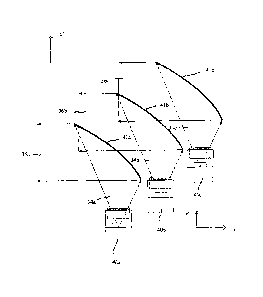
Fig. 6a to 6f show various embodiments of high power laser diode arrays
according to the
present invention including different optical assemblies for slow axis
collimation or focusing
of linear high power laser diodes disposed in parallel with each other under a
predetermined
pitch. In these drawings the high power laser diodes are shown in a top view
onto the end face
of the high power laser diode and along the direction of alignment of the
laser diodes of this
high power laser diode.
As shown in Fig. 6a, the fast-axis collimated output laser beams 34a-34c
generated by the
high power laser diodes 40a-40c as described above are deflected by associated
parabolic
hollow mirrors 41a-41c. In this arrangement the distance from the center of
each parabolic
minor 41a-41c to the respective diode laser of the laser diode 40a-40c is
identical for all
diode lasers 40a-40c. The curvature of these mirrors 41a-41c is such that a
slow-axis
collimation of the output laser beams 34a-34c is achieved in slow axis so that
the deflected
output laser beams 36a-36c are collimated in both fast and slow axis
direction. In other words:
CA 02643923 2015-11-09
27
the respective laser light emitters of the laser diodes 40a-40c are disposed
at the focus of a
respective parabolic hollow mirror 41a-41c. Further, the mirrors 41a-41c and
the high power
laser diodes 40a-40c are disposed in an interleaved, chess-board like manner
so that the
deflected output laser beams 36a-36c are interleaved in a substantially
seamless manner, as
indicated by the resulting schematic beam profile shown in Fig. 6b. As the
individual output
laser beams 36a-36c are substantially collimated in both fast axis and slow
axis direction at
preferably identical divergence angles in slow and fast axis direction, the
resulting beam
profile shown in Fig. 6b exhibits a substantially homogenous intensity
distribution for all
encircled beams with almost 100% fill factor without the need for any (micro-)
optical
components as commonly used in the prior art for rearranging the beams of
state-of-the-art
diode lasers.
According to Fig. 6a three high power laser diodes 40a-40c as described above
are disposed
in parallel with each other and under predetermined non-vanishing distances
between
neighbouring high power laser diodes 40a-40c in three directions. More
specifically, in Fig 6a
the laser diodes 40a-40c are shifted in three directions, namely in two
directions (x', z')
perpendicular to the direction of beam propagation (z') after deflection at
the mirror disposed
on the laser diode substrate (cf. e.g. Fig. 5g) and after fast-axis
collimation and in one
direction (y') parallel to the direction of beam propagation of the fast-axis
collimated output
laser beams 34a-34c after deflection at the mirror disposed on the laser diode
substrate.
In the following it is assumed that the fill rate in fast axis direction (y')
is 50%, which means
that the fast-axis collimated output laser beams, which are emitted at
equidistant spacing and
together form a comb-like pattern, if viewed in cross-section of the laser
light beams, fill 50%
of a rectangular stripe extending in fast axis direction. Based on such a fill
rate of 50% in fast
axis direction (y' = y") in this exemplary embodiment, neighbouring rows of
high power
diode lasers 40a-40c are shifted
(a) in fast axis (y' = y") direction by half a pitch, i.e. by half the
distance between
neighbouring laser light emitters of a laser diode 40a-40c,
(b) in slow axis (x'). direction (before and after beam deflection at the
mirrors disposed on the.
laser substrate) by half the beam width of the slow axis collimated beam 36a-
36c and
(c) in direction of the optical axis after beam deflection at the mirrors
disposed on the laser
substrate (z') for constant distance to the respective parabolic hollow mirror
41a-41a serving
as a slow axis collimator.
CA 02643923 2015-11-09
23
This arrangement of diode lasers and collimation lenses results in a fill rate
of 100% in both
fast and slow axis direction with no additional optics to change the direction
or position of
individual beams as in the prior art.
It is apparent to the expert that other shifts and other fill rates can be
achieved with different
shifts.
It will become apparent to a person skilled in the art that by an appropriate
arrangement and
configuration of the mirrors 41a-41c and the high power laser diodes 40a-40c
it is possible to
obtain a beam profile of an arbitrary shape, e.g. line-shaped, rectangular,
circular, elliptical,
star-shaped. This effect can be used to efficiently image and couple the
output laser beam to
other optical components, such as optical fibres, laser rods (for optical
pumping of secondary
laser sources) or any sort of optical medium.
As will become apparent to a person skilled in the art the high power laser
diodes 40a-40c
shown in Fig. 6a may be disposed on a single substrate, e.g. a common heat
sink, that may be
planar or may have a stepped profile (as described below referring to Fig. 7)
in order to
achieve the pitch between neighbouring high power laser diodes 40a-40c as
shown in Fig. 6a.
Fig. 6c shows another modification where all high power laser diodes 40a-40c
are mounted
on the top surface of a common planar heat sink 6. Further, the parabolic
hollow mirrors 41a-
41c image and deflect the output laser beams 34a-34c into a direction which is
not parallel to
the top surface of the heat sink 6 but extends instead in an oblique manner.
Again the
deflected output laser beams 36a-36c are collimated in both fast and slow axis
direction. Thus,
the laser light emitters in the configuration of Fig. 6c are shifted in two
axes perpendicular to
each other.
According to a further related aspect of the present invention, the parabolic
hollow mirrors
shown in Fig. 6a and Fig. 6c can be integrated into a unitary (one-piece)
substrate, e.g. by
diamond-machining or micro-machining. Preferably, the substrate is of copper
to enable an
effective cooling from the backside close to the optical active surface making
dense stacking
of lenses possible and minimizing thelinal lensing and its associated beam
distortion known
from refractive lens systems operated at high power levels. After forming the
parabolic
CA 02643923 2015-11-09
24
hollow mirrors in such a substrate, the inner surfaces of the hollow mirrors
may be coated
with a high-reflective coating, in order to reduce optical losses as far as
possible. As an
alternative, such an array of hollow mirrors may be press-formed or machined
with other
state-of the-art means for manufacturing lenses or lens arrays into a solid
glass body or into
the top surface of a hollow glass body that can be cooled by forced air
circulating
therethrough.
Such a modification is schematically shown in Fig. 6f. Further advantages of
the reflective
parabolic (slow axis) collimation optic are that the fill rate of the
individual optic can be close
to 100% without the loss of beam quality in contrast to refractive optics,
which show beam
distortion due to the edges of the lens and that parabolic surfaces represent
the ideal optical
surface for minimizing bluiT thus maximizing coupling efficiency into optical
fibers at small
diameters.
Fig. 6d shows another modification where all high power laser diodes 40a-40c
are aligned in a
single plane and where the output fast-axis collimated laser 34a-34c are slow-
axis collimated
by means of refractive lenses 36a-36c, which may also be a lens array. Thus,
the laser light
emitters in the configuration of Fig. 6d are shifted in two axes perpendicular
to each other. As
shown in Fig. 6e by suitably arranging the high power laser diodes 40a-40c and
the slow-axis
collimating lenses 37a-37c in an interleaved manner, the deflected output
laser beams 36a-36c
are interleaved in a substantially seamless manner, as indicated by the
resulting schematic
beam profile shown in Fig. 6e. As the individual output laser beams 36a-36c
are substantially
equally collimated in fast and slow axis direction, the resulting beam profile
shown in Fig. 6e
exhibits a substantially homogenous intensity distribution of the encompassing
beam profile
of the individual beams with substantially equal divergence in slow and fast
axis.
It will become apparent to a person skilled in the art that the divergences of
the individual
beams and the combined beam may be different in both axes to comply with a
specific
application. In a similar matter the number of high power diode lasers and the
number of
diodes comprising one high power diode laser is determined by the beam quality
and spot size
at the workpiece upon focusing the collimated beam.
Fig. 6f and 6g show in a side view and a perspective view a high power laser
diode array
according to the present invention. A unitary (single-piece) array 41 of
parabolic hollow
CA 02643923 2015-11-09
mirrors is used for slow-axis collimation of the fast-axis collimated light
beams emitted by the
laser diodes of which only three are denoted by reference numerals 40a-c in
these drawings to
thereby deflect and image the fast and slow axis collimated light beams in an
interleaved
manner so as to generate a substantially homogenous output laser beam profile
50 (cf. Fig.
5 6h) consisting of a plurality of fast and slow axis collimated laser
beams 51 of substantially
rectangular shape and interleaved in a seamless manner.
It will become apparent to a person skilled in the art that by an appropriate
arrangement and
configuration of the slow-axis collimating lenses 36a-36c and the high power
laser diodes
10 40a-40c it is possible to obtain a beam profile of an arbitrary shape,
e.g. line-shaped,
rectangular, circular, elliptical, star-shaped. This effect can be used to
efficiently image and
couple the output laser beam to other optical components, such as optical
fibres, laser rods
(for optical pumping of secondary laser sources) or any sort of optical
medium.
15 As an example of an application of a high power laser diode array of the
present invention, -
Fig. 6i illustrates the focussing of an output laser beam 50 of the high power
laser diode array
as described above onto the entrance aperture 62 of an optical fibre by means
of a focussing
optics, generally denoted as 60. As shown in the right-hand part of Fig. 6i
the output laser
beam 50 consists of a plurality of substantially rectangular-shaped individual
laser beams 51
20 that are collimated both in fast and slow axis by the optical
arrangement described above with
reference to Fig. 5a to 5h. Within the circle denoted in the right-hand part
of Fig. 6i with
reference numeral 50, which corresponds to the substantially circular entrance
aperture 62 of
the optical fibre, the individual laser beams 51 are interleaved in a
substantially seamless
manner, i.e. fill out the entire circle 50. As will become apparent from the
schematic drawing
25 in the right-hand part of Fig. 6i, the chess-board like interleaving of
the individual fast and
slow axis collimated laser beams according to the present invention enables
filling out
arbitrary cross-sectional geometric profiles, e.g. in the example of Fig. 6i
the circle 50.
Fig. 7 shows a high power laser diode array according to another embodiment of
the present
invention. The array comprises a wedge-shaped substrate 6. On the right-hand
side of the
substrate 6 a plurality of step-like laser diode support portions 9a ¨ 9c are
framed, on the
surface of which submounts are individually positioned. On the surface of each
submount, a
laser diode is mounted. For a precise positioning of these components,
precision mounting
tools, as outlined above, are used. Thus, the individual laser light emitters
of the high power
CA 02643923 2015-11-09
26
laser diode 40 on the right-hand side of substrate 6 are offset relative to
each other both in fast
axis and slow axis direction at equal spacings. In front of the exit facet of
each laser light
emitter there is provided a fast axis collimating means 70, which is
individually positioned
and aligned.
On the opposite, i.e. left-hand side of substrate 6 a corresponding number of
step-like portions
71a-71c are provided. Edges of these portions 71a-71c are concavely curved to
act as hollow-
mirrors 72a-72c for slow axis collimation or focussing of the fast axis
collimated laser beams
74. At the same time the fast axis collimated laser beams 74 are deflected by
90 degrees. The
deflected fast and slow axis collimated laser beams 75 are then combined via
mirror 73 to
form a line-shaped output laser beam profile (not shown) consisting of a
plurality of fast and
slow axis collimated or focussed output laser beams arranged adjacent to each
in a seamless
mariner in one dimension with an optical fill factor of 100% or close to 100%.
As will become apparent to a person skilled in the art, several of such high
power laser diode
arrays, as described with reference to Fig. 7, can be combined to form an
output laser beam
profile consisting of a plurality of fast and slow axis collimated or focussed
output laser
beams arranged adjacent to each in a seamless manner in two dimensions, at
arbitrary shape,
with an optical fill factor of 100% or close to 100%.
Fig. 8 shows a high power laser diode array according to still another
embodiment of the
present invention. As shown in Fig. 8, the diode lasers 40a-40c each of the
type as described
above with reference to Fig. 4a to 5h emit fast axis collimated laser beams
34a-34c that are
aligned along (in this example) three single rows, the laser light emitters of
each row being
disposed at equidistant spacings between neighbouring laser light emitters.
According to Fig.
8 the hollow parabolic mirrors 41a-41c focus the output laser beams 34a-34c
both in fast axis
direction and slow axis direction onto a single focal point 62. It is apparent
to a person skilled
in the art that each fast and slow axis focusing mirror 41a-4c has a slightly
different focal
length to ensure that all output laser beams are focussed onto the same focal
point 62. The
mirrors 41a-4.1c may be integrated into a single common substrate, as
described above with
reference to Fig. 6f.
CA 02643923 2015-11-09
27
LIST OF REFERENCE NUMERALS
1 submount
2 diode laser chip
3 bond pad for n-contact
4 bond pad for p-contact
5 electric wires for n-contact
6 heat sink
7 mirror
8 power connector
9a-c laser diode support portions
10 carrier / support substrate for fast axis collimating lens (FAC)
11 inner perimeter of spacer and alignment substrate 10
12 outer perimeter of spacer and alignment substrate 10
14 central cut-out portion
16 right cut-out portion
18 gap
22 inward protrusion
23 outward recess
lower recess in bottom surface flower substrate 26
26 lower substrate of spacer and alignment substrate 10
25 27 upper recess in top surface of upper substrate 28
28 upper substrate of spacer and alignment substrate 10
uncollimated light beam
31 optical axis
30 32 collimating lens (fast axis)
33 rear side of collimating lens (fast axis)
34 fast axis collimated light beam
collimating lens (slow axis)
36 fast axis collimated light beam
CA 02643923 2015-11-09
28
37a, 37b, 37c slow-axis collimating lens
40 high power laser diode
40a, 40b, 40c laser diode row
41a, 41b, 41c parabolic mirror
50 output beam profile
51 individual laser beams collimated in slow and fast axis
60 focussing optics
61 focussed output light beam
62 entrance aperture / optical fibre
70 fast axis collimating means
71a-c step portion
72a-c concavely curved reflective surfaces
73 output minor
74 fast axis collimated laser beam
75 slow axis collimated laser beam
101 submount
102 diode laser chip
103 bond pad for n-contact
104 bond pad for p-contact
105 electric wires for n-contact
106 heat sink
107 mirror
116 right cut-out portion
117 first step portion
118 alignment stop (slow axis)
119 second step portion
121 abutment surface
130 transparent spacer
CA 02643923 2015-11-09
29
300 first surface
301 second surface
131 uncollimated light beam
132 optical axis
133 collimating lens (fast axis)
134 fast axis collimated light beam
136 beam superposing means
137 collimating lens (slow axis)
138 collimated light beam