Note : Les descriptions sont présentées dans la langue officielle dans laquelle elles ont été soumises.
CA 02645474 2008-11-28
SILICON CARBONITRIDE ANTIREFLECTIVE COATING
FIELD OF THE INVENTION
This invention relates to silicon solar cells comprisinci an
antireflective and passivation coating that comprises
amorphous silicon carbonitride. The invention also relates
to a process for preparing a silicon solar cell comprising
the antireflective and passivation coating.
BACKGROUND OF THE INVENTION
Plasma enhanced chemical vapour deposition (PECVD) deposited
silicon nitride (SiNX) films [1,2] are widely used to provide
a surface/bulk passivation and an anti-reflection coating
(ARC) oii pho5pl-ioru5 emitters. SiNX Lilitis provide excellent
surtace passivation on the emitter due to their highly
positive fixed charge density, which induce an inversion or
accumulation layer in Si under the SiN,t. The optimum
refractive index of the AR coating layer for an encapsulated
solar cell is about 2.3, which is achievable by using
silicon rich SiNx films. However, such films absorb light at
short wavelengths, thereby reducing quantum efficiency.
Recently, PECVD-deposited SiC,t films have been studied for
the surface passivation of crystalline silicon (c-Si) as
surface recombination velocities (SRV) lower than 30 cm/sec
have been reported at the SiC,t/c-Si interface [3,4].
Silicon carbonitride films have also been shown to provide
low effective surface recombination velocity on n-type
crystalline silicon bulk structures, suggesting good
passivation characteristics [7]. However, it is known iri
the art that selection of a dielectric passivation layer
cannot be based solely on lifetime measurements of such test
structures [8] .
CA 02645474 2008-11-28
Silicon carbonitride films, prepared by hot wire deposition
and comprising carbon concentrations greater than 40%, have
also been investigated as passivation layers [9,10,11]. The
solar cells obtained, however, suffered from poor contact
formation (i.e. less than 74% Fill Factor) and displayed a
strong dependence on firing temperature, passivation quality
of the film degrading at temperatures above 700 C. Firing
temperatures of up to 900 C are often used during solar cell
production.
BRIEF SUMMARY OF THE INVENTION
In one aspect, the present invention provides a silicon
solar cell comprising an antireflective and passivation
coating, which coating comprises amorphous silicon
carbonitride, wherein the amount of carbon in the silicon
carbonitride is from 5 to 25 atomic %.
In a further aspect, the present invention provides a
process for forming a silicon solar cell, comprising
depositing by plasma-enhanced chemical vapour deposition
(PECVD), on a silicon p-n junction, a gaseous mixture
comprising a) one or more gaseous mono-silicon organosilanes
and b) a nitrogen-containing gas.
In still a further aspect, the present invention provides a
solar cell prepared by a process as defined herein.
The above and other features and advantages of the present
invention will become apparent from the following
description when taken in conjunction with the accompanying
figures which illustrate preferred embodiments of the
present invention by way of example.
BRIEF DESCRIPTION OF THE DRAWINGS
Embodiments of the invention will be discussed with
reference to the following Figures:
2
CA 02645474 2008-11-28
Figure 1 displays the chemical composition (0, C, Si and N)
of SiNX and SiC,tNy films as a function of NH3 flow rate.
Figure 2 displays the hydrogen concentration in SiNX and
SiCXNY films as a function of NH3 flow rate.
Figure 3 graphs the calculated photogeneration contours in
mA/cmz as a function of bottom (n=2.6) and top (n=2.0) layer
thicknesses for planar cells under 300-1200 nm, AM1.5G. No
dispersion or absorption in the AR coating is assumed.
Figure 4 displays the JoE values, as a function of NH3 gas
flow rate, for silicon solar cells comprising SiNX and SiCXNY
films on 45 ohm/sq emitters.
Figure 5 displays the pre- and post-firing JoE values, as a
function of NH3 gas flow rate, for silicon solar cells
comprising SiNX and SiCXNY films on 45 ohm/sq emitters.
Figure 6 graphs the surface charge densities of SiNX and
SiCXNY films as a function of NH3 gas flow rate.
Figure 7 displays the pre- and post-firing Lifetime
measurements, as a function of NH3 gas flow rate, for SiNx
and SiCXNy films prepared on 45 ohm/sq emitters.
Figure 8 displays IQE responses and reflectance measurements
of SiNX or SiCXNy antireflective coatings.
Figure 9 graphs the efficiency of silicon solar cells
bearing SiCXNY antireflective coatings as a function of the
carbon concentration in the coating.
Figure 10 graphs the refractive index of SiNX and SiCXNy
films prepared with varying NH3 gas flow rates.
Figure 11 graphs the extinction coefficient of SiNX and
SiCXNY films prepared with varying NH3 gas flow rates.
3
CA 02645474 2008-11-28
Figure 12 graphs the Fill Factor values for silicon solar
cells comprising SiNX and SiC,tNY films on 45 ohm/sq emitters,
at varying NH3 gas flow rates.
Figure 13 graphs the Fill Factor values for silicon solar
cells comprising SiN,t and SiC,,Ny films on 60 ohm/sq emitters,
at varying NH3 gas flow rates.
Figure 14 graphs the efficiency of silicon solar cells
bearing SiCXNY antireflective coatings, prepared by remote
plasma-enhanced chemical vapor deposition, as a function of
the carbon concentration in the coating.
DETAILED DESCRIPTION OF THE INVENTION
The present invention describes a silicon solar cell
comprising an antireflective and passivation coatirig, which
coating comprises amorphous silicon carbonitride, wherein
the amount of carbon in the silicon carbonitride is from 5
to 25 atomic %, for example from 5 to 20 atomic %, from 5 to
19 atomic %, from 5 to 15 atomic %, from 10 to 19 atomic %,
or from 14 to 18 atomic %. The amorphous silicon
carbonitride is referred to herein as SiCXNy. The silicon
carbonitride also comprises bonded or interstitial hydrogen
atoms, the presence of which is understood in the term
S i CXNy .
A silicon solar cell, as recited herein, means a wide area
electronic device that converts solar energy into
electricity by the photovoltaic effect, the device
comprising a large-area p-n junction made from silicon. The
cell also comprises ohmic metal-semiconductor contacts which
are made to both the n-type and p-type sides of the solar
cell, and one or more coatings that act as a passivation and
antireflective coating. Examples of silicon solar cells
include amorphous silicon cells [12], amorphous silicon-
polycrystalline silicon tandem cells [13], silicon-
4
CA 02645474 2008-11-28
silicon/germanium tandem cells [14], string ribbon cells
[15] , PERC cells [16] , and PERL cells [17].
ARC composition
In one embodiment, the atomic % range for Si in the SiCXNY
ARC is from about 25% to about 70%, for example from about
30% to about 60%, from about 30 to about 35%, or from about
31% to about 34%.
In another embodiment, the atomic % range for H in the SiCXNY
ARC is from about 10% to about 40%, for example from about
15% atomic % to about 35%, from about 20 to about 30% or
from about 22 to about 28%.
In another embodiment, the atomic % range for N in SiCXNy is
up to about 65%, for example frunt about 10o to about 600,
from about 20% to about 40%, or trom about 25% to about 35%.
In a further embodiment, the film can also comprise other
atomic components as dopants. For example, the doped-film
can comprise F, Al, B, Ge, Ga, P, As, 0, In, Sb, S, Se, Te,
In, Sb or a combination thereof.
The thickness of the film can be selected based on the
optical and physical characteristics desired for the
prepared ARC. In one embodiment, the thickness is selected
in order to obtain a reflection minima at a light wavelength
of about 600-650nm. For example a refractive index of 2
with a thickness of 75nm can be considered optimum, although
small variations in thickness may not greatly affect the
refractive index. In one embodiment, the SiCXNy ARC will
have thickness from about 50 to about 160nm, e.g. from about
50 to about 100nm or from about 70 to about 80nm.
In one embodiment, the antireflective coating comprises only
a SiCXNylayer. In another embodiment, the antireflective
coating comprises a multiplicity of layers, at least one of
5
CA 02645474 2008-11-28
which is a SiCXNy layer as described herein. In yet another
embodiment, the antireflective coating comprises a SiCXNY
layer as described herein, which layer displays a graded
refractive index through its thickness.
Conversion efficiency
A solar cell's energy conversion efficiency is the
percentage of power converted (from absorbed light to
electrical energy) and collected, when a solar cell is
connected to an electrical circuit. Standard test
conditions (STC) specify a temperature of 25 C and an
irradiance of 1000 W/m2 with an air mass 1.5 (AM1.5)
spectrum. These correspond to the irradiance and spectrum
of sunlight incident on a clear day upon a sun-facing 370-
tilted surface with the sun at an angle of 41.810 above the
horizon. This condition approximately represents solar noon
near the spring and autumn equinoxes in the continental
United States with surface of the cell aimed directly at the
sun. Thus, under these conditions a solar cell of 12%
efficiency with a 100 cm2 (0.01 mZ) surface area can be
expected to produce approximately 1.2 watts of power.
The losses of a solar cell may be broken down into
reflectance losses, thermodynamic efficiency, recombination
losses and resistive electrical loss. The overall
efficiency is the product of each of these individual
losses. Due to the difficulty in measuring these parameters
directly, other paxameters are measured instead, such as:
Quantum Efficiency, Voc ratio, Jsc, J , JoE and Fill Factor.
Reflectance losses are a portion of the Quantum Efficiency
under "External Quantum Efficiency". Recombination losses
make up a portion of the Quantum Efficiency, Voc ratio, and
Fill Factor (FF). Resistive losses are predominantly
categorized under Fill Factor, but also make up minor
portions of the Quantum Efficiency and Voc ratio.
6
CA 02645474 2008-11-28
Quantum efficiency
When a photon is absorbed by a solar cell it is converted to
an electron-hole pair. This electron-hole pair may then
travel to the surface of the solar cell and contribute to
the current produced by the cell; such a carrier is said to
be collected. Alternatively, the carrier may give up its
energy and once again become bound to an atom within the
solar cell without reaching the surface; this is called
recombination, and carriers that recombine do not contribute
to the production of electrical current.
Quantum efficiency refers to the percentage of photons that
are converted to electric current (i.e., collected carriers)
when the cell is operated under short circuit conditions.
Quantum efficiency can be quantified by the equal.iosi:
Quantum efficiency = Jsc - Voc - FF/Pin
External quantum efficiency is the fraction of incident
photons that are converted to electrical current, while
internal quantum efficiency is the fraction of absorbed
photons that are converted to electrical current.
Mathematically, internal quantum efficiency is related to
external quantum efficiency by the reflectance of the solar
cell; given a perfect anti-reflection coating, they are the
same.
Voc ratio
VoC depends on Jsc and JoE, where JSc is the short circuit
current density and JoE is the emitter saturation current
density. Mathematically, Voc = (kT/q) - ln (Jsc/JoE+ 1) . JoE can
depend on Auger recombination losses, defects related
recombination losses and the level of emitter doping. Due
to recombination, the open circuit voltage (Voc) of the cell
will be below the band gap voltage (Vg) of the cell. Since
7
CA 02645474 2008-11-28
the energy of the photons must be at or above the band gap
to generate a carrier pair, cell voltage below the band gap
voltage represents a loss. This loss is represented by the
ratio of Voc divided by Vg.
Maximum-power point
A solar cell may operate over a wide range of voltages (V)
and currents (I). By increasing the resistive load on an
irradiated cell continuously from zero (a short circuit) to
a very high value (an open circuit) one can determine the
maximum-power point, the point that maximizes VxI; that is,
the load for which the cell can deliver maximum electrical
power at that level of irradiation (the output power is zero
in both the short circuit and open circuit extremes).
Fill Factor and Rshunt
Another defining term in the overall behaviour of a solar
cell is the Fill Factor (FF). This is the ratio of the
actual obtainable power (maximum power point) divided by the
theoretically obtainable power (based on the open circuit
voltage (Voc) and the short circuit current (Isc) . The Fill
factor is thus defined as (VpIp) I(Voclsc) , where Imp and Vmp
represent the current density and voltage at the maximum
power point.
Rshunt (RSH) is also indicative of cell performance since, as
shunt resistance decreases, the flow of current diverted
through the shunt resi-stor increases for a given level of
junction voltage, producing a significant decrease in the
terminal current I and a slight reduction in Voc. Very low
values of RSH will produce a significant reduction in Voc.
Much as in the case of a high series resistance, a badly
shunted solar cell will take on operating characteristics
similar to those of a resistor.
8
CA 02645474 2008-11-28
High values for Fill Factor, together with high Rshunt
values, indicate that quality of the contact formed on solar
cell is high. While quality of the contact will also depend
in part on other factors, such as the nature of the p-n
emitter and the process used to form the contact, a major
contributor to Fill Factor is the nature of the
antireflective coating, through which the contact must be
made. As an estimate, a 0.5% improvement in Fill Factor
leads to - 0.1% increase in cell efficiency, and such an
increase in efficiency can be equated to a substantial
increase in profitability for solar cell production.
Passivation
It is beneficial for the long-term stability of the
efficiency of a solar cell that the surface passivation
capability of the solar cell does not degrade under extended
exposure to sunlight. The ARC should therefore be able to
passivate defects in the surface or near-surface region of
the solar cell due to earlier processing steps (e.g. saw
damage; etch damage, dangling bonds, etc...). Poorly
passivated surfaces reduce the short circuit current (Isc),
the open circuit voltage (Voc), and the internal quantum
efficiency, which in turn reduces the efficiency of the
solar cell. The ARC film can reduce the recombination of
charge carriers at the silicon surface (surface
passivation), which is particularly important for high
efficiency and thin solar cells (e.g. cells having a
thickness <200 m). Bulk passivation is also important for
multicrystalline solar cells, and it is believed that high
hydrogen content in the ARC film can induce bulk passivation
of various built-in electronic defects (impurities, grairi
boundaries, etc.)in the multicrystalline (mc) silicon bulk
material. The SiCXNy films of the present invention
naturally contain bonded and/or interstitial hydrogen atoms,
and they display good passivation characteristics.
9
CA 02645474 2008-11-28
Characterization of the SiCXN,, ARC
The Si/C/N chemical composition and hydrogen content of SiNX
and SiCxNY films, as a function of NH3 flow rate during film
deposition, are displayed in Figures 1 and 2, respectively.
Other deposition parameters including the flow rate of
silicon source, deposition temperature, pressure, and plasma
power were fixed for all the depositions shown in the
Figures. From Figures 1 and 2, it can be seen that with
increases in NH3 flow, the carbon and hydrogen contents in
the SiCXNy film decrease and the nitrogen content increases.
The silicon fraction was found to be constant regardless of
the NH3 flow rate, meaning that the carbon composition can be
varied by adjusting the flow rate of NH3 gas, without
affecting the silicon composition. Accordinqly, the
chemical compositions of the dielectric films approach to
those of the SiN, coating as the NH3 flow rate increases.
From Figure 2, it can be noted that hydrogen content in some
embodiments of SiCXNy is higher than in SiN,t, indicating that
SiCXNy may supply enough hydrogen to passivate defects in
bulk silicon during contact firing.
In one embodiment, the SiCXNY ARC of the invention can have a
refractive index (n) at a wavelength of 630nm of 1.8 to .2.3,
for example a refractive index of 2.05, and an extinction
coefficient (k) at a wavelength of 300nm of less than 0.01,
for example less than 0.001. From Table 7 in the
experimental section, it can be seen that the refractive
index is reduced with in6reased nitrogen content in the
films. It is expected that wider range of refractive index
can be achieved by either changing the nature of the gaseous
reactants used to prepare the ARC, and/or the NH3 gas flow
rate.
CA 02645474 2008-11-28
The SiCXNy can also be combined to form a double layer ARC.
As shown in Figure 3, the double layer ARC should provide
improvement in short circuit current density (J5C)
JoE values were also measured on 45 ohm/sq textured emitters
in order to study electrical properties of SiC,sNy films
coated with different NH3 gas flow rates and compared with
those of SiNX films, as shown in Figures 4 and 5. The JoE
values between SiNX and SiCXNy films were fairly constant,
regardless of NH3 gas flow rate used in their preparation,
indicating that SiCXNy can provide an excellent cell
performance when used for the front surface passivation of
Si solar cells. As shown in Figure 6, the surface charge
densities (QFB) in the SiCXNY films after annealing was
measured to be slightly lower than that of the SiNX film.
The surface charge density plays a critical role to the
surface passivation as well as to device performance [5,6].
However, from Figure 7, where lifetime measurements for
SiCXN, and SiNX films (pre- and post-firing) are displayed,
we see that passivation obtained with the SiC,,NX film is
similar to or greater than the passivation for the SiNX film.
From these results, it would appear that the comparable JoE
values shown in Figures 4 and 5 for SiCXNX and SiNx films are
in both cases caused by highly positive surface charge
density and relatively high hydrogen concentration.
The SiCXNY films were applied to solar cell fabrication to
compare their performance with that of a conventional PECVD
SiNx film. Cell efficiencies above 16.8% were achieved on
the solar cells with SiCXNY AR coatings, and both the SiNX
and SiCXNy of films provided comparable JSC and Vpc values.
It would appear that the comparable JSc and Vo, can be
attributed to high-quality optical and electrical properties
of the SiCXNY films. However, improvements in Fill Factor
(FF) and Rshunt (Rsx) values were observed for SiCxNY films.
Without being bound by theory, it is believed that the
11
CA 02645474 2008-11-28
higher FF and RSH values shown by the SiCXNY AR coatings may
be related to the etching behaviour of the glass frit in the
Ag paste used to make the better contacts. During contact
formation, lead borosilicate glass melts and etches the
antireflective coating. A redox reaction between PbO and Si
also takes place, forming liquid Pb, which then dissolves Ag
and Si to etch the emitter surface. The presence of carbon
in the antireflective coating likely affects this redox
reaction, which potentially provides better contact
formation between metal (Ag) and semiconductor (Si), as
suggested by the increase Fill Factor and Rshunt values
observed.
The internal quantum efficiency (IQE) and reflectance values
of the solar cells with the SiNX and SiCXNy ARCs were also
measured (Figure 8). From short and long wave length
responses, SiCXNy films were shown to provide a high surface
passivation quality without hurting bulk lifetime.
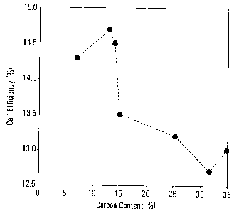
The efficiency of silicon solar cells comprising SiCXNy
antireflective coatings as a function of the carbon content
is displayed in Figures 9 and 14. From the Figures, it can
be seen that there appears to be an advantageous range for
the carbon content in the SiCXNy film.
Preparation of the SiCXNy ARC
In one aspect, the invention provides a process for
preparing SiCXNy anti-reflective coatings of the invention.
In one embodiment, the ARC film can be prepared by plasma
enhanced chemical vapour deposition of gaseous species
comprising Si, C, N and H atoms.
While it is possible to combine all of the required Si, C, N
and H atoms within a single gaseous species, two or more
12
CA 02645474 2008-11-28
gases, collectively comprising the required atomic species,
can be combined and reacted under PE-CVD conditions.
In one embodiment, the required C and Si atoms are contained
in separate gases, while in another embodiment the C and Si
atoms are contained in a single gaseous species. For
example, the SiCXNy ARC can be prepared from a mixture of
SiH4, a gaseous source of nitrogen (e.g. NH3 or N2) , and a
gaseous hydrocarbon (e.g. methane), which gases are mixed
and exposed to an energy enhanced CVD instrument.
Alternately, a gaseous organosilicon compounds (e.g. an
organosilane and/or an organopolycarbosilane), mixed with a
gaseous source of nitrogen (e.g. NH3, N2, or NC13) and
exposed to PE-CVD conditions can yield the SiCxNY ARC. The
gaseous organosilicon compounds can be obtained commercially
in gas form (and admixed if required), or they can be
prepared (optionally in-situ) from solid precursors.
13
CA 02645474 2008-11-28
Gaseous organosilicon compounds from solid precursors
In one embodiment, the gaseous organosilanes and/or
organopolycarbosilanes can be obtained from thermal
decomposition/rearrangement (i.e. pyrolysis) or
volatilisation of a solid organosilane source. The solid
organosilane source can be any compound that comprises Si, C
and H atoms and that is solid at room temperature and
pressure.
The solid organosilane source may, in one embodiment, be a
silicon-based polymer comprising Si-C bonds that are
thermodynamically stable during heating in a heating
chamber. In one embodiment, the silicon-based polymer has a
monomeric unit comprising at least one silicon atom and two
or more carbon atoms. The monomeric unit may further
comprlse additional elements such as N, 0, F, or a
combination thereof. In another embodiment, the polymeric
source is a polysilane or a polycarbosilane.
The polysilane compound can be any solid polysilane compound
that can produce gaseous organosilicon compounds when
pyrolyzed, i.e. chemical decomposition of the solid
polysilane by heating in an atmosphere that is substantially
free of molecular oxygen. In one embodiment, the solid
polysilane compound comprises a linear or brariched
polysilicon chain wherein each silicon is substituted by one
or more hydrogen atoms, C1-C6 alkyl groups, phenyl groups or
-NH3 groups. In a further embodiment, the linear or brariched
polysilicon chain has at least one monomeric unit comprising
at least one silicon atom and one or more carbon atoms. In
another embodiment, the linear or branched polysilicon chain
has at least one monomeric unit comprising at least one
silicon atom and two or more carbon atoms.
14
CA 02645474 2008-11-28
Examples of solid organosilane sources include silicon-based
polymers such as polydimethylsilane (PDMS) and
polycarbomethylsilane (PCMS), and other non-polymeric
species such as triphenylsilane or nonamethyltrisilazane.
PCMS is commercially available (Sigma-Aldrich) and it can
have, for example, an average molecular weight from about
800 Daltons to about 2,000 Daltons. PDMS is also
commercially available (Gelest, Morrisville, P.A. and Strem
Chemical, Inc., Newburyport, M.A.) and it can have, for
example, an average molecular weight from about 1,100
Daltons to about 1,700 Dalton. Use of PDMS as a source
compound is advantageous in that (a) it is very safe to
handle with regard to storage and transfer, (b) it is air
and moisture stable, a desirable characteristic when using
large vo1umPS of a compound in an industrial environment.,
(c) no corrosive components are g?nerat.Pd in an Pf.fliient
stream resulting from PDMS being exposed to CVD process
conditions, and (d) PDMS provides its own hydrogen supply by
virtue of its hydrogen substituents.
In another embodiment, the solid organosilane source may
have at least one label component, the type, proportion and
concentration of which can be used to create a chemical
"fingerprint" in the obtained film that can be readily
measured by standard laboratory analytical tools, e.g.
Secondary Ion Mass Spectrometry (SIMS), Auger Electron
Spectrometry (AES), X-ray photoelectron spectroscopy (XPS).
In one embodiment, the solid organosilane source can contain
an isotope label, i.e. a non-naturally abundant relative
amount of at least one isotope of an atomic species
contained in the solid organosilane source, e.g. C13 or C14
This is referred to herein as a synthetic ratio of isotopes.
CA 02645474 2008-11-28
Pyrolysis/volatilization of the solid precursor
In one embodiment, the gaseous organosilicon species are
formed by pyrolysis of the solid organosilane source in a
heating chamber. The solid source may be added to the
heating chamber in a batch or continuous manner as a powder,
pellet, rod or other solid form. Optionally, the solid
organosilane source may be mixed with a second solid polymer
in the heating chamber. In batch addition, the solid
organosilane source compound may be added, for example, in
an amount in the range of from 1 mg to 10 kg, although
larger amounts may also be used.
In one embodiment the heating chamber is purged, optionally
under vacuum, after the solid organosilane source has been
added, to replace the gases within the chamber with an inert
gas, such as argon or helium. The chamber can be purged
before heating is commenced, or the temperature within the
chamber can be increased during, or prior to, the purge.
The temperature within the chamber during the purge should
be kept below the temperature at which evolution of the
gaseous species commences to minimise losses of product.
The pyrolysis step can encompass one or more different types
of reactions within the solid. The different types of
reactions, which can include e.g.
decomposition/rearrangement of the solid organosilane into a
new gaseous and/or liquid organosilane species, will depend
on the nature of the solid organosilane source, and these
reactions can also be promoted by the temperature selected
for the pyrolysis step. Control of the above parameters can
also be used to achieve partial or complete volatilisation
of the solid organosilane source instead of pyrolysis (i.e.
instead of decomposition/rearrangement of the organosilane
source). The term "pyrolysis", as used herein, is intended
to also capture such partial or complete volatilizatioin.
16
CA 02645474 2008-11-28
For embodiments where the solid organosilane source is a
polysilane, the gaseous species can be obtained through a
process as described in U.S. provisional application S/N
60/990,447 filed on November 27, 2007, the disclosure of
which is incorporated herein by reference in its entirety.
The heating of the solid organosilane source in the heating
chamber may be performed by electrical heating, UV
irradiation, IR irradiation, microwave irradiation, X-ray
irradiation, electronic beams, laser beams, induction
heating, or the like.
The heating chamber is heated to a temperature in the range
of, for example, from about 50 to about 700 C, from about 100
to about 700 C, from about 150 to about 700 C, from about 200
Uo about 700 C, from about 250 to about 700 C, from about 300
to about 700 C, from about 350 to about 700 C, from about 400
to about 700 C, from about 450 to about 700 C, from about 500
to about 700 C, from about 550 to about 700 C, about 600 to
about 700 C, from about 650 to about 700 C, from about 50 to
about 650 C, from about 50 to about 600 C, from about 50 to
about 550 C, from about 50 to about 500 C, from about 50 to
about 450 C, from about 50 to about 400 C, from about 50 to
about 350 C, from about 50 to about 300 C, from about 50 to
about 250 C, from about 50 to about 200 C, from about 50 to
about 150 C, from about 50 to about 100 C, from about 100 to
about 650 C, from about 150 to about 600 C, from about 200 to
about 550 C, from about 250 to about SO0 C, from about 300 to
about 450 C, from about 350 to about 400 C, from about 475 to
about 500 C, about 50 C, about 100 C, about 150 C, about
200 C, about 250 C, about 300 C, about 350 C, about 400 C,
about 450 C, about 500 C, about 550 C, about 600 C, about
650 C, or about 700 C. A higher temperature can increase the
rate at which the gaseous compounds are produced from the
solid organosilane source.
17
CA 02645474 2008-11-28
In one embodiment, the heating chamber is heated at a rate
of up to 150 C per hour until the desired temperature is
reached, at which temperature the chamber is maintained. In
another embodiment, the temperature is increased to a first
value at which pyrolysis proceeds, and then the temperature
is changed on one or more occasion, e.g. in order to vary
the rate at which the mixture of gaseous compound is
produced or to vary the pressure within the chamber.
In one embodiment the temperature and pressure within the
heating chamber are controlled, and production of the
gaseous species can be driven by reducing the pressure, by
heating the organosilane source, or by a combination
thereof. Selection of specific temperature and pressure
values for the heating chamber can also be used to control
the nature of the gaseous species obtained.
In the embodiment where the solid organosilane source is a
polysilane, one possible pyrolysis reaction leads to the
formation of Si-Si crosslinks within the solid polysilane,
which reaction usually takes place up to about 375 C.
Another possible reaction is referred to as the Kumada
rearrangement, which typically occurs at temperatures
between about 225 C to about 350 C, wherein the Si-Si
backbone chain becomes a Si-C-Si backbone chain. While this
type of reaction is usually used to produce a non-volatile
product, the Kumada re-arrangement can produce volatile
polycarbosilane oligomers, silanes and/or methyl silanes.
While the amount of gaseous species produced by way of the
Kumada rearrangement competes with the production of non-
volatile solid or liquid polycarbosilane, the production of
such species, while detrimental to the overall yield, can
prove a useful aspect of the gas evolution process in that
any material, liquid or solid, that is left in the heating
chamber is in some embodiments turned into a harmless and
18
CA 02645474 2008-11-28
safe ceramic material, leading to safer handling of the
material once the process is terminated.
Gaseous organosilicon species
Generally, the gaseous organosilicon species prepared from
solid organosilanes comprise a mixture of volatile fragments
of the organosilane. In the embodiment where the solid
organosilane precursor is a polysilane, the gaseous species
are a mixture of gaseous organosilicon compounds, i.e.
compounds comprising silicon, carbon and hydrogen atoms that
are in the gas phase at 20 C and 20 psi.
In one embodiment, the mixture of gaseous organosilicon
compounds substantially comprises one or more gaseous
silanes (i.e. gaesous compounds comprising a single silicon
atom). These are also referred to herein as gaseous mono-
silicon organosilanes, examples of such include methyl
silane, dimethyl silane, trimethyl silane and tetramethyl
silane.
In one embodiment, the gaseous mixture can also optionally
comprise small amounts (e.g. less than 10%) of gaseous
multi-silicon species, such as gaseous polysilanes, or
gaseous polycarbosilanes. By gaseous polysilane is meant a
compound comprising two or more silicon atoms wherein the
silicon atoms are covalently linked (e.g. Si-Si), and by
gaseous polycarbosilane is meant a compound comprising two
or more silicon atoms wherein at least two of the silicon
atoms are linked through a non-silicon atom (e.g. Si-CHZ-Si).
Examples of gaseous polycarbosilanes can have the formula:
Si (CH3)n(H)m- L (CH2) -Si (CH3)p(H)q]X-Si (CH3) n' (H)m'
wherein n, m, n' and m' independently represent an integer
from 0 to 3, with the proviso that n + m = 3 and n' + m' =
3; p and q independently represent an integer from 0 to 2,
19
CA 02645474 2008-11-28
with the proviso that p + q = 2 for each silicon atom; and x
is an integer from 0 to 3. Further examples of gaseous
polycarbosilanes include [Si (CH3) (H) 2] -CH2- [Si (CH3) 2 (H) ] ,
[Si (CH3) 2 (H) ] -CH2- [Si (CH3) 2 (H) ] , [Si (CH3) 3] -CH2- [Si (CH3) Z (H)
] ,
[Si (CH3) 2 (H) ] -CH2- [Si (CH3) 2] -CH2- [Si (CH3) 3] , [Si (CH3) (H) 2] -
CHz-
[Si (CH3) 2] -CHz- [Si (CH3) (H) 2] , [Si (CH3) (H) z] - CHz - [Si (CH3) z] --
CH2-
[Si (CH3) 2 (H) ] , [Si (CH3) 2 (H) ] -CH2- [Si (CH3) 2] -CH2- [Si (CH3) 2 (H)
]
[Si (CH3) 2 (H) ] -CH2- [Si (CH3) 2] -CH2- [Si (CH3) 2] -CH2- [Si (CH3) 2 (H)
]
[Si (CH3) (H) 2] -CH2- [Si (CH3) z] -CH2- [Si (CH3) z] -CHz- [Si (CH3) z (H) ]
,
[Si (CH3) (H) 2] -CHz- [Si (CH3) 2] -CH2- [Si (CH3) z] -CH2- [Si (CH3) (H) 2]
and [Si (H) 3] -CH2- [Si (CH3) 2] -CH2- [Si (CH3) 2] -CH2- [Si (CH3) (H) 2] In
one embodiment, the gaseous species is a mixture
comprising from 20 to 45 wt.% methylsilane, from 35 to 65
wt.% dimethylsilane, from 5 to 15 wt.% trimethylsilane, and
optionally up to 10 wt.% gaseous carbosilane species.
After forming the gaseous species, it may be used
immediately or stored under appropriate temperature and
pressure conditions for later use. The process may be
interrupted at this stage since the heating chamber may be
external to the reactor.
Addition of a reactant gas
The gaseous species used to form the SiCXNY may be mixed with
a reactant gas in the deposition chamber, in a gas mixing
unit, or when pyrolysis is used to obtain the gaseous
species, in the heating chamber. In one embodiment, the
reactant gas may be in the form of a gas that is
commercially available, and the gas is provided directly to
the system. In another embodiment, the reactant gas is
produced by heating a solid or liquid source comprising any
number of elements, such as 0, F, or a combination thereof.
In one example, the reactant gas may be an oxygen-based gas
such as CO, 02, 03, CO2 or a combination thereof.
CA 02645474 2008-11-28
In an embodiment, the reactant gas may also comprise F, Al,
B, Ge, Ga, P, As, In, Sb, S, Se, Te, In and Sb in order to
obtain a doped SiCXNy film.
Deposition chamber
When it is desired to form a film, a substrate is placed
into a deposition chamber, which is evacuated to a
sufficiently low pressure, and the gaseous species and
optionally a carrier gas are introduced continuously or
pulsed. Any pressure can be selected as long as the energy
source selected to effect the deposition can be used at the
selected pressure. For example, when plasma is used as the
energy source, any pressure under which plasma can be formed
is suitable. In embodiments of the present invention the
pressure can be from about 50 to about 4000 mTorr, from
about 100 to about 500 mTorr, from about 150 to about 500
mTorr, from about 200 to about
500 mTorr, from about 200 to about 500 mTorr, from about 250
to about 500 mTorr, from about 300 to about 500 mTorr, from
about 350 to about 500 mTorr, from about 400 to about 500
mTorr, from about 450 to about 500 mTorr, from about 50 to
about 450 mTorr, from about 50 to about 400 mTorr, from
about 50 to about 350 mTorr, from about 50 to about
300 mTorr, from about 50 to about 250 mTorr, from about 50
to about 200 mTorr, from about 50 to about 150 mTorr, from
about 50 to about 100 mTorr, from about 100 to about
450 mTorr, from about 150 to about 400 mTorr, from about 200
to about 350 mTorr, from about 250 to about 300 mTorr, from
about 50 mTorr to about 5 Torr, from about 50 mTorr to about
4 Torr, from about 50 mTorr to about 3 Torr, from about
50 mTorr to about 2 Torr, from about 50 mTorr to about
1 Torr, about 50 mTorr, about 100 mTorr, about 150 mTorr,
about 200 mTorr, about 250 mTorr, about 300 mTorr, about.
350 mTorr, about 400 mTorr, about 450 mTorr, about
21
CA 02645474 2008-11-28
500 mTorr, about 1 Torr, about 2 Torr, about 3 Torr, about
4 Torr, or about 5 Torr.
The substrate is held at a temperature in the range of, for
example, from about 25 to about 500 C, from about 50 to about
500 C, from about 100 to about 500 C, from about 150 to about
500 C, from about 200 to about 500 C, from about 250 to about
500 C, from about 300 to about 500 C, from about 350 to about
500 C, from about 400 to about 500 C, from about 450 to about
500 C, from about 25 to about 450 C, from about 25 to about
400 C, from about 25 to about 350 C, from about 25 to about
300 C, from about 25 to about 250 C, from about 25 to about
200 C, from about 25 to about 150 C, from about 25 to about
100 C, from about 25 to about 50 C, from about 50 to about
450 C, from about 100 to about 400 C, from about 150 to about
350 C, from about 200 to about 300 C, about 25 C, about 50 C,
about 100 C, about 150 C, about 200 C, about 250 C, about
300 C, about 350 C, about 400 C, about 450 C, or about 500 C.
Any system for conducting energy induced chemical vapour
deposition may be used for the method of the present
invention, and other suitable equipment will be recognised
by those skilled in the art. The typical equipment, gas
flow requirements and other deposition settings for a
variety of PECVD deposition tools used for commercial
coating solar cells can be found in True Blue, Photon
International, March 2006 pages 90-99 inclusive, the
contents of which are enclosed herewith by reference.
The energy source in the deposition chamber may be, for
example, electrical heating, hot filament processes, UV
irradiation, IR irradiation, microwave irradiation, X-ray
irradiation, electronic beams, laser beams, plasma, or RF.
In a preferred embodiment, the energy source is plasma, and
examples of suitable plasma deposition techniques include
plasma enhanced chemical vapour deposition (PECVD), radio
22
CA 02645474 2008-11-28
frequency plasma enhanced chemical vapour deposition (RF-
PECVD), electron-cyclotron-resonance plasma-enhanced
chemical-vapour deposition (ECR-PECVD), inductively coupled
plasma-enhanced chemical-vapour deposition (ICP-ECVD),
plasma beam source plasma enhanced chemical vapour
deposition (PBS-PECVD), or combinations thereof.
Furthermore, other types of deposition techniques suitable
for use in manufacturing integrated circuits or
semiconductor-based devices may also be used.
For embodiments where the energy used during the deposition
is plasma, e.g. for PE-CVD, characteristics of the obtained
film may be controlled by suitably selecting conditions for
(1) the generation of the plasma, (2) the temperature of the
substrate, (3) the power and frequency of the reactor, and
(4) the type and amount of gaseous species introduced into
the deposition chamber.
Configuration of heating and deposition chambers
In those embodiments where the gaseous organosilicon species
is obtained from the pyrolysis of a solid source, the
process may be carried with a variety of system
configurations, such as a heating chamber and a deposition
chamber; a heating chamber, a gas mixing unit and a
deposition chamber; a heating chamber, a gas mixing unit and
a plurality of deposition chambers; or a plurality of
heating chambers, a gas mixing unit and at least one
deposition chamber. In a preferred embodiment, the
deposition chamber is within a reactor and the heating
chamber is external to the reactor.
For high throughput configurations, multiple units of the
heating chamber may be integrated. Each heating chamber in
the multiple-unit configuration may be of a relatively small
scale in size, so that the mechanical construction is simple
23
CA 02645474 2008-11-28
and reliable. All heating chambers may supply common gas
delivery, exhaust and control systems so that cost is
similar to a larger conventional reactor with the same
throughput. In theory, there is no limit to the number of
reactors that may be integrated into one system.
The process may also utilize a regular mass flow or pressure
controller to more accurately deliver appropriate process
demanded flow rates. The gaseous species may be transferred
to the deposition chamber in a continuous flow or in a
pulsed flow.
The process may in some embodiments utilize regular tubing
without the need of special heating of the tubing as is the
case in many liquid source CVD processes in which heating
the tubing lines is cssential to elimiriate source vapour
condensation, or edrliei decumposition of the source.
EXAMPLES
The following examples are provided to illustrate the
invention. It will be understood, however, that the
specific details given in each example have been selected
for purpose of illustration and are not to be construed as
limiting the scope of the invention. Generally, the
experiments were conducted under similar conditions unless
noted.
The antireflective coatings were deposited using a "Coyote"
PECVD system manufactured by Pacific Western. The PECVD
deposition was carried out at a substrate temperature of
425 C to 475 C, a pressure of 2 Torr, a power of 150W, and
an RF power frequency of 50kHz. The flow of gaseous
organosilicon compound into the PECVD instrument was
maintained at 300sccm (silane equivalent mass flow
conditions), and the flow of ammonia was maintained between
24
CA 02645474 2008-11-28
1500-4500 sccm. Separate depositions were also made using a
Roth and Rau AK400 remote plasma tool.
Optical properties of the dielectric films were
characterized by a spectroscopic ellipsometer (Woollam Co.).
The composition of the dielectric films was analyzed by XPS
(X-ray photoelectron spectroscopy) and Elastic Recoil
Detection (ERD). Saw damage on the as-cut wafers was
removed by etching in potassium hydroxide (KOH) solution
followed by anisotropic etching in the mixture of KOH and
isopropyl alcohol (IPA) for texturing. The textured silicon
wafers were cleaned in 2: 1: 1 H20: H202: H2SO4 and 2: 1: 1 H20:
H202: HC1 solutions followed by phosphorus diffusion in a
quartz tube to form 45 and 60 0/sq emitters.
For comparative purposes, a cunventional SiNX AR coating
layer wiLh a L2iic:kness of 75 nm and a refractive index of
-2.05 was deposited in the same low-frequency (50 KHz) PECVD
reactor (Coyote) . The SiNX depositions were made at a
SiH4:NH3 ratio of 300:3000 sccm.
Silicon carbonitride films were deposited in the same
chamber using ammonia and gas generated from a solid PDMS
source. The solid source was heated inside a sealed
pressure vessel. The gas evolved from the PDMS was supplied
to the PECVD reactor via standard silane mass flow
controllers (MFC) and flow was controlled assuming the same
correction factor as for silane. No gas condensation
problems were observed in the gas delivery system. The
carrier lifetimes in the wafers and emitter saturation
current density (JoE) of the diffused emitters were measured
using Sinton's quasi-steady-state photoconductance (QSSPC)
tool. The charge density in the dielectrics was measured
using SemiTest SCA-2500 surface charge analyzer, which
allows contactless and non-destructive measurement of the
flat band equivalent charge density (QFB, the total charge
CA 02645474 2008-11-28
density at the flat band condition) in the dielectric of
interest. The front and rear contacts were formed by
screen-printing commercial Ag paste and Al paste,
respectively, followed by firing in an IR metal belt
furnace.
The hydrogen concentration in the SiCXNy films was measured
by Elastic Recoil Detection (ERD).
The efficiency of the solar cells was measured using a
custom-made I-V system, with the solar cell illuminated. at
one sun conditions, 1,000W/cmz. The cell was kept at 25 C.
The equipment was calibrated with a solar cell obtained from
the National Renewable Energy Laboratory of the US
Department of Energy.
Example 1
Boron doped Czochralski (Cz) silicon wafers of 1-3 ohm=cm
base resistivity and 230 m thickness were used as a
substrate for 149 cm2 screen printed solar cells. The
results obtained with depositions made on a 45 0/sq emitter
are shown in Table 1. For comparative pursposes, SiN,, layers
were prepared from silane and NH3. No optimizations were
made for the SiCXNy depositions; the optimized process
conditions for SiNX depositions were used. The dielectric
layers prepared were fired at a temperature of 850 C for 5
seconds following deposition.
26
CA 02645474 2008-11-28
Table 1 Electrical measurements on 45 0/sq emitters
SiH4 or
polymer NH3 Voc Jsc Fill Efficiency n Rseries Rshunt
flow (sccm) (mV) (mA/cm2 ) Factor (~) factor (S2cm2 ) (S2cm' )
(sccm)
300 (SiH4) 3000 623.0 34.92 0.783 17.0 1.07 0.781 4665
300
(polymer) 3000 622.0 34.80 0.780 16.9 1.07 0.799 24922
300
(polymer) 4500 621.7 34.50 0.782 16.8 1.03 0.868 248209
Example 2
In a manner similar to Example 1, solar cells were prepared
with a 60 0/sq emitter, and results are shown in Table 2.
Again, film thicknesses were not optimized for the SiNX film,
and not the SiCXNY films.
27
CA 02645474 2008-11-28
Table 2 Electrical measurements on 60 Q/sq emitters
SiH4 or
polymer NH3 Voc Jsc Fill Efficiency n Rseries Rshunt
flow (sccm) (mV) (mA/cmz ) Factor M factor (Qcm2 ) (Qcm' )
(sccm)
300
(SiH4) 3000 620 36.1 0.763 17.1 1.07 1.077 2208
300
(polymer) 1500 618 35.6 0.772 17.0 1.02 1.043 40250
300
(polymer) 3000 618 35.8 0.766 17.0 1.06 1.044 24335
300
(SiH4) 3000 619.7 35.90 75.6 16.82 1.08 1.101 2423
300
(polymer) 1500 616.9 35.51 76.9 16.84 1.05 1.05 28532
300
(polymer) 3000 616.7 35.71 76.7 16.89 1.06 1.04 58267
Example 3
Further solar cells were prepared with 45 0/sq emitters,
with an optimized SiCXNY film thickness for the obtained
refractive index. Table 3 provides a comparison of the SiN,t
and SiCXNy films prepared.
28
CA 02645474 2008-11-28
Table 3 Optimized measurements on 45 S2/sq emitters
SiH4 or
polymer NH3 Voc Jsc Fill Efficiency n Rseries Rshunt
flow (sccm) (mV) (mA/cm2 ) Factor (%) factor (S2cm2 ) (S2cm2 )
(sccm)
300 (SiH4) 3000 620 34.99 0.772 16.76 1.14 0.791 2080
300
(polymer) 3500 618 35.48 0.780 17.11 1.00 0.882 7541
Example 4
Further solar cells were prepared with a Roth and Rau AK400
remote plasma tool, varying the carbon concentration in the
deposited SiCXNY films. The efficiency of the prepared
cells, as a function of the carbon content, is shown in
Figure 14.
Composition of the SiCXNY films
Auger analysis of the 0, C, N and Si content of SiNX and
SiCXNY dielectric films as described herein is provided in
Table 4. These results are also displayed graphically in
Figure 1.
Table 4 Auger analsysis of SiNX and SiC,tN films
SiCN SiN
NH3 flow(sccm)
1500 2000 2500 3000 4500
0 2.8 2.7 3.1 3.0 2.6 3.8
(at.%)
C 24.7 21.0 17.5 15.9 13.1 0.0
(at. o)
29
CA 02645474 2008-11-28
N 41.7 44.9 48.1 50.6 53.3 60.4
(at.%)
S 30.7 31.4 31.3 30.2 30.6 35.5
(at.%)
Hydrogen concentration analysis of SiN,t and SiCxNy films, by
Elastic Recoil Detection (ERD), is provided in Figure 2.
Hydrogen concentrations of SiNX and SiC,,Ny films are also
provided in table 5:
Table 5 Hydrogen concentrations of SiNX and SiCXNy films
T SiN SiCN SiCN SiCN SiCN SiCN
NH3 @1500 NH3 @2000 NH3 @2500 NH3 @3000 NH3 @4500
sccm sccm sccm sccm sccm
H 11.8 15.4 12.7 11.3 8.8 9.0
(at.%)
The combined Auger and ERD analysis are provided in Table 6.
Table 6 Chemical composition of SiN,, and SiCXNY films
SiCN SiN
NH3 flow(sccm)
1500 2000 2500 3000 4500
H 15.4 12.7 11.3 8.8 9.0 11.8
(at.%)
O 2.4 2.4 2.7 2.7 2.4 3.4
(at.%)
C 20.9 18.3 15.5 14.5 11.9 0.0
(at.%)
N 35.3 39.2 42.7 46.1 48.5 53.3
(at.%)
S 26.0 27.4 27.8 27.5 27.8 31.3
(at. %)
CA 02645474 2008-11-28
Characterization of optical properties
The refractive index (n) and extinction coefficient (k) of
SiNX and SiCXNY dielectric films as a function of NH3 flow
rate are summarized in Table 7. The n and k values were
measured at the wavelengths of 630 nm and 300 nm,
respectively.
Table 7. Refractive indices (n) and extinction coefficient
(k) of SiNX and SiCXN,, films as a function of NH3 flow rate.
S i NH3 n k
Film
Source (sccm) at 630 nm at 300 nm
SiNX SiH4 3000 2.04 0.026
SiCXNy PDMS 1500 1.97 0.052
SiCXNy PDMS 2000 1.95 0.031
SiCXNy PDMS 2500 1.94 0.027
Graphical representation of the refractive index and
extinction coefficient of SiNX and SiCXNy dielectric layers,
obtained by spectroscopic ellipsometry (VASE), are provided
in Figures 10 and 11.
In a separate experiment, it was found that the refractive
index can be increased up to -(2.3) as the NH3 flow rate is
decreased during the production of SiCXNy. The base process
without NH3 flow was nominally stoichiometric SiC since there
is no nitrogen source. However, since the screen printed
contact formation process used was optimized for
conventional SiNX films, NH3 flow rates in the range of 1500-
2500 sccm were used as these yield similar Si/N compositions
to that of the SiNX film. By adjusting the source
31
CA 02645474 2008-11-28
composition and gas flow rates, SiCXNY films with a
refractive index range of 1.94-1.97 at 630 nm wavelength
were obtained.
32
CA 02645474 2008-11-28
Characterization of electrical properties
Boxplot graphs of Fill Factor values measured for SiC,,Ny and
SiN,t solar cells prepared on 45 and 60 ohm/sq emitters are
provided in Figures 12 and 13. Fill Factor enhancements are
observed both in terms of percentage increases and narrowing
of distribution for the SiCXNY antireflective coatings over
the SiNXfilms, indicating improvements in contact
properties.
J E values were measured for SiN,t and SiC,tNy solar cells
prepared on 45 ohm/sq textured emitters and the results are
presented in Figure 4. All the samples were fired in an RTP
chamber at 850 C for 5 sec before J E measurement. A boxplot
of J E values for pre- and post-fired SiNX and SiC,tNY films is
also provided in Figure 5.
Figure 6 shows the surface charge densities (QFB) in SiNX and
SiC,,Ny dielectric films after annealing in an RTP chamber at
850 C for 5 sec. The surface charge density in the SiCXNy
film was measured to be in the range of 1.58-1.77x10¹²/cmz
which is slightly lower than that of SiNX film
(1.89x10¹²/cmz) .
Internal quantum efficiency (IQE) and reflectance values
measured on the two types of cells were measured and are
presented in Figure 8. A boxplot of lifetime measurements
for pre- and post-fired SiNX and SiCXNY films is provided in
Figure 7.
33
CA 02645474 2008-11-28
All publications, patents and patent applications cited in
this specification are herein incorporated by reference as
if each individual publication, patent or patent application
were specifically and individually indicated to be
incorporated by reference. The citation of any publication
is for its disclosure prior to the filing date and should
not be construed as an admission that the present invention
is not entitled to antedate such publication by virtue of
prior invention.
Although the foregoing invention has been described in some
detail by way of illustration and example for purposes of
clarity of understanding, it is readily apparent to those of
ordinary skill in the art in light of the teachings of this
invention that certain changes and modifications may be made
thereto without departing from the spirit or scope of the
appended claims.
It must be noted that as used in this specification and the
appended claims, the singular forms "a", "an", and "the"
include plural reference unless the context clearly dictates
otherwise. Unless defined otherwise all technical and
scientific terms used herein have the same meaning as
commonly understood to one of ordinary skill in the art to
which this invention belongs.
34
CA 02645474 2008-11-28
REFERENCES
1. R.Hezel and R.Schorner, "Plasma Si nitride-a promising
dielectric to achieve high-quality silicon MIS/IL solar
cells", J. Appl. Phys., vol.52, p.3076, 1981
2. J.Schmidt, T.Lauinger, A.G.Aberle, and R. Hezel, "Record
low surface recombination velocities on low resistivity
silicon solar cell substrate", 25thIEEE PVSC, Washington,
DC, p.413, 1996.
3. S. W. Glunz, S. Janz, M. Hofmann, T. Roth, and G.
Willeke,"Surface passivation of silicon solar cells using
amorphous silicon carbide layers", 4th WCPEC, Waikola, p.4,
2006.
4. I.Martin, M. Vetter, A. Orpella, and J. Puigdollers,
A.Cuevas and R.Alcubilla, "Surface passivation of p-type
crystalline Si by plasma enhanced chemical vapor deposited
amorphous SiCx :H films", App. Phys. Lett, vol.79, no.14,
p.2199, 2001.
5. V.Meemongkolkiat, D.S. Kim, and A.Rohatgi, "Si02-based
spin-on dielectrics for back surface passivation of p-type
Si solar cells", 22nd European PVSEC, Italy, 2007.
6. S.D.Wolf, G.Agostinelli, G.Beaucarne and P.Vitanov,
"Influence of stoichiometry of direct plasma-enhanced
chemical vapor deposited SiNX films and silicon substrate
surface roughness on surface passivation", J.Appl.Phys.,
vol.97, p.63303, 2005.
7. Vetter et al. "IR-study of a-SiCX:H and a-SiCXNy:H films
for c-Si surface passivation", Thin Solid Films 451-452
(2004) 340-344.
8. Glunz et al. "Comparison of Different Dielectric
Passivation in Industrially Feasible High-Efficiency
CA 02645474 2008-11-28
Crystalline Silicon Solar Cells", Presented at the 20th
European Photovoltaic Solar Energy Conference and
Exhibition, 6-10 June 2005, Barcelona.
9. Limmanee et al. "Effect of thermal annealing on the
properties of a-SiCN:H films by hot wire chemical vapour
deposition using hexmethyldisilazane", Thin Solid Films 516
(2008) 652-655.
10. Limmanee et al. "Effect of nitrogen addition on the
properties of a-SiCN:H films using hexmethyldisilazane",
Mater. Res. Soc. Symp. Proc. Vol. 989 (2007).
11. Limmannee et al. "Study of the structural properties of
a-SiCN:H films using hexamethyldisilazane for high-quality
silic:oli passivation", Proceeding of IEEE 4th World Conference
on Photovoltaic Energy Conversion, Hawai, U.S.A, May 7-12,
2006.
12.M. Zeman, J. Krc "Optical and electrical modeling of
thin-film silicon solar cells", Journal of Materials
Research Volume: 23 No 4 Pages: 889-898.
13. D.E. Carlson, K. Rajan, R.R. Arya, F. Willing, L. Yang
"Advances in amorphous silicon photovoltaic technology",
Journal of Materials Research Volume: 13 No 10 Pages: 2754-
2762.
14. J. Yang, A. Banerjee, and S. Guha "Triple-junction
amorphous silicon alloy solar cell with 14.6% initial and
13.0% stable conversion efficiencies", Appl. Phys. Lett. 70,
2975 (1997).
15. K. Nakayashiki, B. Rounsaville, V. Yelundur, D.S. Kim,
A. Rohatgi, R. Clark-Phelps, and J.I. Hanoka "Fabrication
and analysis of high-efficiency String Ribbon Si solar
-30 cells", Solid-State Electron. 50, 1406 (2006).
36
CA 02645474 2008-11-28
16. Mark Kerr, Jan Schmidt, Andres Cuevas "Comparison of the
open circuit voltage of simplified PERC cells passivated
with PECVD silicon nitride and thermal silicon oxide",
Progress in Photovoltaics: Research and Applications Volume
8 Issue 5, Pages 529 - 536.
17. J.Zhao, A Wang, P Campbell, M.A.Green "22.7% efficient
PERL silicon solar cell module with a textured front
surface", Photovoltaic Specialists Conference, 1997.,
Conference Record of the Twenty-Sixth IEEE 29 Sep-3 Oct 1997
Pages 1133 - 1136.
37