Note : Les descriptions sont présentées dans la langue officielle dans laquelle elles ont été soumises.
CA 02645813 2009-08-04
MASK PROGRAMMABLE ANTI-FUSE ARCHITECTURE
FIELD OF THE INVENTION
[001] The invention is directed to non-volatile memories. More specifically,
the
invention is directed to mask programming of non-volatile memory cells.
BACKGROUND OF THE INVENTION
[002] Over the past 30 years, anti-fuse technology has attracted significant
attention
of many inventors, IC designers and manufacturers. An anti-fuse is a structure
alterable to a
conductive state, or in other words, an electronic device that changes state
from not
conducting to conducting. Equivalently, the binary states can be either one of
high resistance
and low resistance in response to electric stress, such as a programming
voltage or current.
There have been many attempts to develop and apply anti-fuses in
microelectronic industry,
but the most successful anti-fuse applications to date can be seen in FGPA
devices
manufactured by Actel and Quicklogic, and redundancy or option programming
used in
DRAM devices by Micron. Anti-fuse technology is well known in the art, and
example anti-
fuse transistors are shown in Figures 1 to 5b.
[003] Anti-fuse memory is one type of one-time programmable (OTP) memory in
which the device can be permanently programmed (electrically) with data once.
This data is
programmed by an end user for a particular application. There are several
types of OTP
memor-y cells which can be used. OTP memories provide users with a level
flexibility since
any data can be programmed.
[004] Anti-fuse memory can be utilized in all one time programmable
applications,
including RF-ID tags. RF-ID tagging applications are gaining more acceptance
in the
industry, particularly in sales, security, transport, logistics, and military
applications for
example. The simplicity and full CMOS compatibility anti-fuse memory allows
for application
-1-
CA 02645813 2009-08-04
of the RF-ID tag concept to integrated circuit manufacturing and testing
processes.
Therefore, IC manufacturing productivity can be increased by utilizing anti-
fuse memory in
combination with an RF communication interface on every wafer and/or every die
on the
wafer allowing for contact-less programming and reading chip specific or wafer
specific
information during IC manufacturing and packaging, as well as during printed
circuit board
assembly.
[005] Figure 1 is a circuit diagram illustrating the basic concept of an anti-
fuse
memory cell, while Figures 2 and 3 show the planar and cross-sectional views
respectively,
of the anti-fuse memory cell shown in Figure 1. The memory cell of Figure 1
includes a pass,
or access transistor 10 for coupling a bitline BL to a bottom plate of anti-
fuse device 12. A
wordline WL is coupled to the gate of access transistor 10 to turn it on, and
a cell plate
voltage Vcp is coupled to the top plate of anti-fuse device 12 for programming
anti-fuse
device 12.
[006] It can be seen from Figures 2 and 3 that the layout of access transistor
10 and
anti-fuse device 12 is very straight-forward and simple. The gate 14 of access
transistor 10
and the top plate 16 of anti-fuse device 12 are constructed with the same
layer of polysilicon,
which extend across active area 18. In the active area 18 underneath each
polysilicon layer,
is formed a thin gate oxide 20, also known as a gate dielectric, for
electrically isolating the
polysilicon from the active area underneath. On either side of gate 14 are
diffusion regions
22 anci 24, where diffusion region 24 is coupled to a bitline. Although not
shown, those of skill
in the art will understand that standard CMOS processing, such as sidewall
spacer formation,
lightly doped diffusions (LDD) and diffusion and gate silicidation, can be
applied. While the
classical single transistor and capacitor cell configuration is widely used, a
transistor-only
anti-fuse cell is further desirable due to the semiconductor array area
savings that can be
obtained for high-density applications. Such transistor-only anti-fuses niust
be reliable while
simple to manufacture with a low cost CMOS process.
[007] Figure 4a shows a cross-sectional view of an anti-fuse transistor that
can be
manufactured with any standard CMOS process. Variants of this anti-fuse
transistor are
disclosed in commonly owned U.S. Patent No. 7,402,255, and commonly owned U.S.
Patent
Publication No. 2007/0257331. In the presently shown example, the anti-fuse
transistor is
almost identical to a simple thick gate oxide, or input/output MOS
-2-
CA 02645813 2008-12-23
WO 2008/077240 PCT/CA2007/002287
transistor with one floating diffusion terminal. The disclosed anti-fuse
transistor, also termed
a split-channel capacitor or a half-transistor, can be reliably programmed
such that the fuse
link between the polysilicon gate and the substrate can be predictably
localized to a
particular region of the device. The cross-section view of Figure 4a is taken
along the
channel length of the device, which in the presently described example is a p-
channel
device. The channel is generally understood to be the area underneath an
overlying
polysilicon gate, having a length defined by edges of the polysilicon gate
adjacent respective
diffusion regions.
[009] Anti-fuse transistor 30 includes a variable thickness gate oxide 32
formed on
the substrate channel region 34, a polysilicon gate 36, sidewall spacers 38, a
field oxide
region 40 a diffusion region 42, and an LDD region 44 in the diffusion region
42. A bitline
contact 46 is shown to be in electrical contact with diffusion region 42. The
variable thickness
gate oxide 32 consists of a thick oxide and a thin gate oxide such that a
portion of the
channel length is covered by the thick gate oxide and the remaining portion of
the channel
length is covered by the thin gate oxide. Generally, the thin gate oxide is a
region where
oxide breakdown can occur. The thick gate oxide edge meeting diffusion region
42 on the
other hand, defines an access edge where gate oxide breakdown is prevented and
current
between the gate 36 and diffusion region 42 is to flow for a programmed anti-
fuse transistor.
While the distance that the thick oxide portion extends into the channel
region depends on
the mask grade, the thick oxide portion is preferably formed to be at least as
long as the
minimum length of a high voltage transistor formed on the same chip.
[0010] In this example, the diffusion region 42 is connected to a bitline
through a
bitline contact 46, or other line for sensing a current from the polysilicon
gate 36, and can be
doped to accommodate programming voltages or currents. This diffusion region
42 is formed
proximate to the thick oxide portion of the variable thickness gate oxide 32.
To further protect
the edge of anti-fuse transistor 30 from high voltage damage, or current
leakage, a resistor
protection oxide (RPO), also known as a salicide protect oxide, can be
introduced during the
fabrication process to further space metal particles from the edge of sidewall
spacer 38. This
RPO is preferably used during the salicidiation process for preventing only a
portion of
diffusion region 42 and a portion of polysilicon gate 36 from being salicided.
It is well known
that salicided transistors are known to have higher leakage and therefore
lower breakdown
voltage. Thus having a non-salicided diffusion region 42 will reduce leakage.
Diffusion region
-3-
CA 02645813 2009-08-04
42 can be doped for low voltage transistors or high voltage transistors or a
combination of
the two resulting in same or different diffusion profiles.
[0010] A simplified plan view of the anti-fuse transistor 30 is shown in
Figure 4b.
Bitline contact 46 can be used as a visual reference point to orient the plan
view with the
corresponding cross-sectional view of Figure 4a. The active area 48 is the
region of the
device where the channel region 34 and diffusion region 42 is formed, which is
defined by an
OD mask during the fabrication process. The dashed outline 50 defines the
areas in which
the thick gate oxide is to be formed via an OD2 mask during the fabrication
process. More
specifically, the area enclosed by the dashed outline 50 designates the
regions where thick
oxide is to be formed. OD simply refers to an oxide definition mask that is
used during the
CMOS process for defining the regions on the substrate where the oxide is to
be formed, and
OD2 refers to a second oxide definition mask different than the first. Details
of the CMOS
process steps for fabricating anti-fuse transistor 30 will be discussed later.
According to an
embodiment of the present invention, the thin gate oxide area bounded by edges
of the
active area 48 and the rightmost edge of the OD2 mask, is minimized. In the
presently shown
embodiment, this area can be minimized by shifting the rightmost OD2 mask edge
towards
the parallel edge of active area 48. Commonly owned U.S. Patent Publication
No.
2007/0257331, the contents of which are incorporated by reference, describes
alternate
single transistor anti-fuse memory cells which can be used in a non-volatile
memory array.
Two transistor anti-fuse memory cells are known in the art, as shown in the
example of
Figures 5a and 5b.
[0011] Figure 5b shows a planar view of a two-transistor anti-fuse memory cell
60
having a minimized thin gate oxide area that can be manufactured with any
standard CMOS
process, according to an embodiment of the present invention. Figure 5a shows
a cross-
sectiorial view of the memory cell 60 of Figure 5b, taken along line B-B. Two-
transistor anti-
fuse memory cell 60 consists of an access transistor in series with an anti-
fuse transistor.
The access transistor includes a polysilicon gate 62 overlying a thick gate
oxide 64, which
itself is formed over the channel 66. On the left side of the channel 66 is a
diffusion region 68
electrically connected to a bitline contact 70. On the right side of the
channel 66 is a common
diffusion region 72 shared with the anti-fuse transistor. The anti-fuse
transistor includes a
polysilicon gate 74 overlying a thin gate oxide 76, which itself is formed
over the channel 78.
The thick gate oxide 64 can correspond to that used for high voltage
transistors while the thin
-4-
CA 02645813 2009-08-04
gate oxide 76 can correspond to that used for low voltage transistors. The
dashed outline 77
defines the areas in which the thick gate oxide is to be formed via an OD2
mask during the
fabrication process. More specifically, the area enclosed by the dashed
outline 77 designates
the regions where thick oxide is to be formed. While the right-most edge of
dashed outline 77
is showed to be substantially aligned with an edge of the side-wall spacer
adjacent to
polysilicon gate 74, those skilled in the art will understand that this edge
can be positioned
anywhere between the sidewall spacers of polysilicon gates 62 and 74. It is
well known that
polysilicon gates 62 and 74 can be independently controlled, or alternatively
can be
connected to each other as shown in Figure 5b. In the example of Figure 5b,
both polysilicon
gates 62 and 74 are part of the same polysilicon structure, and connected to a
wordline
through wordline contact 80. Both diffusion regions 68 and 72 can have LDD
regions, which
can be identically doped or differently doped, depending on the desired
operating voltages to
be used. Commonly owned U.S. Patent Publication No. 2007/0257331 describes
alternate
two-transistor anti-fuse memory cells which can be used in a non-volatile
memory array.
[0012] The programming speed of OTP memories is relatively slow, since each
programming cycle will attempt to program a certain number of data words at
the same time.
Following each programming cycle is a program verify cycle to ensure that the
data words
were successfully programmed. Any bits that do not pass the program verify
step are
reprogrammed. This process continues until all the memory cell states have
been
successfully programmed.
[0013] There are applications where the same data is to be programmed in every
OTP rnemory. Boot block data for exarnple, can be the same in every chip in
the batch, while
the actual user data can be different. The boot block can be programmed by the
end user, or
by the vendor. In either case, a significant number of program cycles will be
required for
programming this boot block data to all the OTP memory devices in the batch.
There may be
other applications where a portion of every OTP memory device will store the
same data. In
some cases, this data is not intended to be accessible or known by the end
user, thereby
requiring programming before delivery to the end user for integration into
their systems.
However, this pre-programming will add time overhead, which is undesired.
[0014] Mask ROM memory is a class of non-volatile memory which is programmed
with data during the chip manufacturing stage. In a chip manufacturing stage,
masks are
-5-
CA 02645813 2008-12-23
WO 2008/077240 PCT/CA2007/002287
used to define which memory cells in the memory array are to be permanently
turned off.
Since programming is performed during chip manufacturing, the effective
"programming"
speed is extremely high. This technique is cost effective with economies of
scale, due to the
capital cost of the mask sets that are required. For example, known video
gaming console
game cartridges used Mask ROM chips to store game data, and the fast
manufacturing of
the chips allowed for large quantities of game cartridges to be sold worldwide
with minimal
time.
[0016] Unfortunately, Mask ROM is programmable only at the manufacturing
stage,
and does not give end users the ability to program their own data to the
memory device. U.S.
Patent No. 7,102,926 discloses a memory device whereby a Mask ROM memory array
is
paired with an electrically erasable programmable read only memory (EEPROM).
However,
there is additional complexity and cost associated with such a device because
the
manufacturing process for Mask ROM differs substantially from that of an
EEPROM.
Furthermore, the additional cost for an EEPROM device is not economical for
applications in
which data is only programmed to the memory once.
[0017] It is, therefore, desirable to provide a low cost OTP memory device
which is
mask programmable while having user programmability.
SUMMARY OF THE INVENTION
[0018] It is an object of the present invention to obviate or mitigate at
least one
disadvantage of prior OTP memories. More specifically, it is an object of the
present
invention provide an anti-fuse memory that is both mask programmable and
electrically
programmable.
[0019] In a first aspect, the present invention provides a hybrid memory
having
electrically programmable and mask programmed memory cells arranged in rows
and
columns. The hybrid memory array includes a row of electrically programmable
anti-fuse
memory cells and a row of mask programmed anti-fuse memory cells. Each
electrically
programmable anti-fuse memory cell is connected to a bitline and has a
predetermined
layout and a gate oxide structure. Each mask programmed anti-fuse memory cell
is
connected to the bitline connected to one electrically programmable anti-fuse
memory cell,
and has substantially the predetermined layout and the gate oxide structure.
Each mask
programmed anti-fuse memory cell represents one logic state by being
selectively mask
-6-
CA 02645813 2008-12-23
WO 2008/077240 PCT/CA2007/002287
programmed to have a permanent coupling to a voltage supply. Each mask
programmed
anti-fuse memory cell can represent another logic state by being selectively
mask
programmed to omit a channel region. According to an embodiment of the present
aspect,
the row of mask programmed anti-fuse memory cells includes an electrically
programmable
status memory cell, and the electrically programmable status memory cell is
identical to each
of the electrically programmable anti-fuse memory cells. According to further
embodiments of
the present aspect, the permanent coupling can include a contact electrically
connected to
the voltage supply and coupled to the bitline when a corresponding wordline is
activated; a
diffusion region connected to the voltage supply and coupled to the bitline
when a
corresponding wordline is activated; and a diffusion region connected to a
corresponding
wordline and coupled to the bitline when the corresponding wordline is driven
to the voltage
supply.
[0020] In a further embodiment, the row of mask programmed anti-fuse memory
cells
are coupled to a wordline receiving a programming voltage, the hybrid memory
further
including a program lock circuit coupled to the wordline for inhibiting the
programming of the
row of mask programmed anti-fuse memory cells. The program lock circuit
includes a mask
programmable inhibit circuit coupled to the wordline and programmed to a lock
state for
changing the programming voltage to a voltage level ineffective for
programming in response
to the wordline at the programming voltage.
[0021] In another embodiment of the present aspect, each of the electrically
programmable anti-fuse memory cells and each of the mask programmable anti-
fuse
memory cells includes an access transistor and an electrically programmable
anti-fuse
transistor. The access transistor has a first diffusion region coupled to the
bitline and a first
polysilicon gate. The electrically programmable anti-fuse transistor is in
series with the
access transistor and has a second diffusion region shared with the access
transistor, and a
second polysilicon gate. The gate oxide structure including a thick gate oxide
under the first
polysilicon gate and a thin gate oxide under the second polysilicon gate. In
the present
embodiment, the first polysilicon gate is drivable to a read voltage during a
read operation,
and the second polysilicon gate is drivable to a programming voltage during a
programming
operation. In an alternate embodiment, the first polysilicon gate and the
second polysilicon
gate are electrically coupled to each other and to a wordline drivable to a
programming
voltage. The permanent coupling can include a contact electrically connected
to the voltage
-7-
CA 02645813 2008-12-23
WO 2008/077240 PCT/CA2007/002287
supply and coupled to the bitline when the access transistor is activated; a
third diffusion
region connected to the voltage supply and coupled to the bitline when the
access transistor
and the electrically programmable anti-fuse transistor are activated; and a
third diffusion
region connected to a diffusion line, the diffusion line being coupled to the
second polysilicon
gate. Furthermore, each mask programmed anti-fuse memory cell representing
another logic
state is selectively mask programmed to omit a channel region.
[0022] In yet another embodiment of the present aspect, each of the
electrically
programmable anti-fuse memory cells and each of the mask programmable anti-
fuse
memory cells includes an electrically programmable anti-fuse transistor. The
electrically
programmable anti-fuse transistor has a diffusion region coupled to the
bitline, and a
polysilicon gate. The gate oxide structure including an oxide breakdown region
fusible to
form a conductive channel between the polysilicon gate and a substrate beneath
the gate
oxide structure. The gate oxide structure includes a variable thickness gate
oxide having a
thin gate oxide portion corresponding to the oxide breakdown region. The
permanent
coupling includes another diffusion region connected to the voltage supply,
and coupled to
the bitline when a wordline coupled to the polysilicon gate is activated.
Alternately, the
permanent coupling includes another diffusion region connected to a diffusion
line, the
diffusion line being coupled to the polysilicon gate. Each mask programmed
anti-fuse
memory cell representing another logic state can be selectively mask
programmed to omit a
channel region.
[0023] In a second aspect, the present invention provides a hybrid memory. The
hybrid memory includes an electrically programmable anti-fuse memory cell and
a mask
programmed memory cell. The electrically programmable anti-fuse memory cell
being
connected to a corresponding bitline and a common wordline. The mask
programmed
memory cell is connected to another bitline and the common wordline for
storing a validity bit.
The electrically programmable anti-fuse memory cell includes an electrically
programmable
anti-fuse transistor having a diffusion region coupled to the bitline, and a
polysilicon gate
overlying a gate oxide structure. The gate oxide structure has an oxide
breakdown region
fusible to form a conductive channel between the polysilicon gate and a
substrate beneath
the gate oxide structure. The mask programmed memory cell can either omit a
channel
region underlying the common wordline, or include a permanent coupling to a
voltage supply.
The permanent coupling can include another diffusion region connected to the
voltage
-8-
CA 02645813 2008-12-23
WO 2008/077240 PCT/CA2007/002287
supply, and coupled to the bitline when the wordline coupled to the
polysilicon gate is
activated.
[0024] In an embodiment of the present aspect, the hybrid memory further
includes a
second mask programmed memory cell and a second electrically programmable anti-
fuse
memory cell. The second mask programmed memory cell is connected to the
corresponding
bitline and a second common wordline. The second electrically programmable
anti-fuse
memory cell is connected to the another bitline and the second common
wordline. In an
alternate embodiment of the electrically programmable anti-fuse memory cell,
the electrically
programmable anti-fuse memory cell includes an access transistor and an
electrically
programmable anti-fuse transistor. The access transistor has a first diffusion
region coupled
to the bitline, and a first polysilicon gate. The electrically programmable
anti-fuse transistor is
in series with the access transistor and has a second diffusion region shared
with the access
transistor, and a second polysilicon gate. The gate oxide structure includes a
thick gate oxide
under the first polysilicon gate and a thin gate oxide under the second
polysilicon gate.
[0025] Other aspects and features of the present invention will become
apparent to
those ordinarily skilled in the art upon review of the following description
of specific
embodiments of the invention in conjunction with the accompanying figures.
BRIEF DESCRIPTION OF THE DRAWINGS
[0026] Embodiments of the present invention will now be described, by way of
example only, with reference to the attached Figures, wherein:
Fig. 1 is a circuit diagram of a DRAM-type anti-fuse cell;
Fig. 2 is a planar layout of the DRAM-type anti-fuse cell of Figure 1;
Fig. 3 is a cross-sectional view of the DRAM-type anti-fuse cell of Figure 2
along line x-x;
Fig. 4a is a cross-sectional view of a variable thickness gate oxide anti-fuse
transistor;
Fig. 4b is a planar layout of the variable thickness gate oxide anti-fuse
transistor of Figure 4a;
Fig. 5a is a cross-sectional view of a two-transistor anti-fuse memory cell;
Fig. 5b is a planar layout of the two-transistor anti-fuse memory cell of
Figure
5a;
-9-
CA 02645813 2008-12-23
WO 2008/077240 PCT/CA2007/002287
Fig. 6 is a block diagram of a hybrid one-time programmable and mask
programmed memory, according to an embodiment of the present invention;
Fig. 7a is a plan view layout showing a hybrid memory array having two-
transistor one-time programmable memory cells and two-transistor mask
programmed memory cells, according to an embodiment of the present invention;
Fig. 7b is a plan view layout showing a hybrid memory array having two-
transistor one-time programmable memory cells and two-transistor mask
programmed memory cells, according to an alternate embodiment of the present
invention;
Fig. 7c is a plan view layout showing a hybrid memory array having alternate
two transistor one-time programmable memory cells and two-transistor mask
programmed memory cells, according to the alternative mask programming
technique
of Figure 7a;
Fig. 7d is a plan view layout showing a hybrid memory array having alternate
two transistor one-time programmable memory cells and two-transistor mask
programmed memory cells, according to the alternative mask programming
technique
of Figure 7b;
Fig. 8a is the plan view layout showing a hybrid memory array illustrating an
alternate mask programming technique;
Fig. 8b is the plan view layout showing a hybrid memory array illustrating the
alternative mask programming technique of Figure 8a;
Fig. 9a is a plan view layout showing a hybrid memory array having single
transistor one-time programmable memory cells and single transistor mask
programmed memory cells, according to an embodiment of the present invention;
Fig. 9b is a plan view layout showing an alternate hybrid memory array,
according to an embodiment of the present invention;
Fig. 10a is a plan view layout of single transistor mask programmed memory
cells programmed using an alternative mask programming technique;
Fig. 10b is a plan view layout of two transistor mask programmed memory
cells programmed using the alternative mask programming technique of Figure
10a;
Fig. 11 is a block diagram of a hybrid memory showing circuit details of a
program lock circuit according to an embodiment of the present invention;
-10-
CA 02645813 2008-12-23
WO 2008/077240 PCT/CA2007/002287
Fig. 12a is an example embodiment of a mask programmable transistor
shown in Figure 11;
Fig. 12b is an example embodiment of an alternate mask programmable
transistor;
Fig. 13 is a block diagram of a hybrid memory with such a program lock
circuit, according to another embodiment of the present invention;
Fig. 14 is an example embodiment of mask programmable inverter shown in
Figure 13;
Fig. 15 is a block diagram of a hybrid memory array having a programmable
status array;
Fig. 16a is a plan view layout of a hybrid memory array with a status array
column, according to an embodiment of the present invention;
Fig. 16b is a plan view layout of a hybrid memory array with a status array
column, according to an alternate embodiment of the present invention.
DETAILED DESCRIPTION
[0027] Generally, the present invention provides a memory array having both
mask
programmable and one-time programmable memory cells connected to the wordlines
and
the bitlines. All memory cells of the memory array are configured as one-time
programmable
memory cells. Any number of these one-time programmable memory cells are
convertible
into mask programmable memory cells through mask programming, such as
diffusion mask
programming or contact/via mask programming. Manufacturing of such a hybrid
memory
array is simplified because both types of memory cells are constructed of the
same
materials, therefore only one common set of manufacturing process steps is
required.
Inadvertent user programming of the mask programmable memory cells is
inhibited by a
programming lock circuit. Each row of data can be tagged as invalid by the
user, while mask
programmed data is protected from user invalidation.
[0028] Therefore, the same code can be mask programmed to a large number of
memory devices during the manufacturing process simply by making the
appropriate mask
modifications to the masks used for manufacturing the one-time programmable
memory
device. More specifically, the masks will be modified to effect mask
programming of specific
-11-
CA 02645813 2008-12-23
WO 2008/077240 PCT/CA2007/002287
memory cells of the memory array. After manufacturing, the memory devices can
then be
immediately shipped to users for programming their own data. The overhead for
mask
programming is minimal prior to device fabrication, and far less than the
accumulated time
required for post-manufacturing electrical programming of each memory device.
Furthermore, the mask programmed lock circuit provides security against post-
manufacturing
programming of the mask programmed memory cells.
[0029] Figure 6 is a block diagram of a hybrid one-time programmable and mask
programmed memory, according to an embodiment of the present invention. The
hybrid
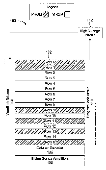
memory 100 includes a hybrid memory array 102, a wordline driver circuit block
104, a
column decoder circuit block 106, a sense amplifier circuit block 108, a
program lock circuit
block 110, and a high voltage switch circuit 112. Those skilled in the art
will understand that
hybrid memory will include other circuit blocks to enable proper operation of
the memory, but
are not shown in Figure 6 as they are not relevant to the embodiments of the
invention. The
hybrid memory array 102 consists of rows and columns of memory cells, where
each row of
memory cells are connected to a common wordline while each column of memory
cells are
connected to a common bitline. In the present embodiment, the one-time
programmable
memory cells and the mask programmed memory cells can have the memory cell
configuration shown in Figures 4a and 4b or Figures 5a and 5b. As illustrated
in Figure 6,
different rows of memory cells will consist of one type of memory cell. For
example, Row 0,
Row 1, Row 9, Row 11, Row 13 and the last row, Row n, will include only one-
time
programmable memory cells (PROM), while Row 2 to Row 8, Row 10, Row 12 and Row
14
will include only mask programmed memory cells (MROM). The different types of
rows can
be interleaved with each other, or grouped together in consecutive rows.
Because the same
type of memory cell is used for both the one-time programmable memory cells
and the mask
programmed memory cells, the wordline pitch and bitline pitch is constant,
thereby
maximizing packing density of the memory array 102.
[0030] The wordline driver circuit block 104 includes individual wordline
drivers for
applying read and program voltages to the wordlines. In the present
embodiment, the read
and program voltages are provided by the high voltage switch circuit 112 in
response to a
control signal indicating that a read or program operation is to be executed.
The high voltage
switch circuit 112 can either generate the read and program voltages, or
couple received
read and program voltages to the wordline driver circuit block 104. Specific
wordlines are
-12-
CA 02645813 2008-12-23
WO 2008/077240 PCT/CA2007/002287
selected for a read or program operation in response to an inputted row
address. The column
decoder circuit block 106 couples any preset number of bitlines to respective
bitline sense
amplifier circuits in sense amplifier circuit block 108, in response to an
inputted column
address. The column decoder circuit block 106 can couple the appropriate bias
voltage
levels to the bitlines for either promoting or inhibiting programming of a one-
time
programmable memory cell. Persons skilled in the art will understand that
there are many
possible architectures and circuit implementations for column decoder circuit
block 106 and
sense amplifier circuit block 108.
[0031] Because a row of mask programmed memory cells are essentially one-time
programmable memory cells, they can be programmed if the bitlines are
appropriately biased
and the wordline is driven to the program voltage level. Therefore, according
to another
embodiment of the present invention, the program lock circuit block 110 is
provided as a
means for inhibiting programming of any row of memory cells, thereby
protecting mask
programmed data stored in that row. This inhibiting is achieved by disrupting
the
programming voltage from reaching the memory cells. Further details of the
program lock
circuit block 110 will follow later.
[0032] Figure 7a is a plan view layout of a portion of the memory array 102 of
Figure
6 illustrating the integration of two-transistor one-time programmable memory
cells and two-
transistor mask programmed memory cells, according to an embodiment of the
present
invention. In the present example, a first row 120 of memory cells connected
to wordline WLi
are one-time programmable memory cells while a second row 122 of memory cells
connected to adjacent wordline WLi+1 are mask programmed memory cells. Each
memory
cell of rows 120 and 122 are two-transistor anti-fuse memory cells having the
same
predetermined layout as shown in Figures 5a and 5b and the same gate oxide
structure. The
dashed outline 123 defines the areas in which the thick gate oxide is to be
formed via an
OD2 mask during the fabrication process, and is analogous to dashed outline 77
shown in
Figure 5a. The gate oxide structure refers to both the thin and thick gate
oxide compositions
of the access transistor and the anti-fuse transistor. In the configuration
shown in Figure 7a,
each pair of memory cells from rows 120 and 122 share a common diffusion
region 124 and
common bitline contact 126. In the present example, one-time programmable
memory cells
of row 120 are electrically programmable, and may or may not have a fuse link
128 formed
when a programming voltage on WLi is applied while the bitline is biased to
ground, VSS or
-13-
CA 02645813 2008-12-23
WO 2008/077240 PCT/CA2007/002287
some other sufficiently low voltage level effective for creating fuse link 128
in the presence of
the program voltage. During a read operation, WLi is driven to VDD and any
memory cell of
row 120 having a fuse link 128 will couple VDD from WLi to its corresponding
bitline. Any
memory cell of row 120 without a fuse link 128 will not have any effect on its
corresponding
bitline.
[0033] The mask programmed cells of row 122 are programmed by connecting the
source diffusion to a high voltage level such as VDD to create the source-
drain path for VDD,
via the channel region underneath the thin gate oxide of the memory cell, such
as thin gate
oxide 76 shown in Figure 5a. The connection is easily made by modifying the
diffusion mask
to include a diffusion region for coupling the selected memory cells of row
122 to a VDD
coupled diffusion line 130. During a read operation, a memory cell of row 122
with the
diffusion region will couple its corresponding bitline to the VDD coupled
diffusion line 130
when the wordline WLi+1 is raised to VDD. In contrast, a memory cell of row
122 with an
absence of the diffusion region cannot couple its corresponding bitline to the
VDD coupled
diffusion line 130, thereby resulting in no effect on the bitline. Therefore,
the reading method
for the memory cells of rows 120 and 122 is the same since the memory cells of
row 120
having a fuse link 128 behave like a memory cell of row 122 having the
diffusion region
connected to the VDD diffusion line 130, and vice versa.
[0034] In the embodiment of Figure 7a, only the diffusions of anti-fuse memory
cells
to be programmed with a particular state are mask programmed to be coupled to
the VDD
coupled diffusion line 130, while anti-fuse memory cells storing the opposite
state remain
unmodified. In the alternate embodiment of Figure 7b, further mask programming
is applied
to those memory cells storing the opposite state. As shown in Figure 7b, the
left-most mask
programmed memory cell of row 122 is mask programmed such that there is no
channel
region beneath polysilicon gate, such as polysilicon gate 74 shown in Figure
5a. In other
words, the channel region is omitted or absent from underneath the polysilicon
gate during
fabrication. This will help prevent the mask programmed memory cells from
accidental
electrical programming. The prevention of accidental electrical programming is
further
enhanced by adjusting the common diffusion region shape, such as common
diffusion
region 72 of Figure 5a, so that it is spaced from the edge of the polysilicon
gate 74.
Accordingly, the mask programmed memory cells of row 122 have substantially
the
-14-
CA 02645813 2008-12-23
WO 2008/077240 PCT/CA2007/002287
predetermined layout as the memory cells of row 120, where the only difference
is the
presence or absence of the channel region and connection to the VDD diffusion
line 130.
[0035] Figure 7c shows an alternate embodiment of the hybrid memory array
shown
in Figure 7a. In the embodiment of Figure 7c, memory cells 120 and 122 share a
common
polysilicon cell plate 129 carrying a cell plate voltage VCP and a common
polysilicon
wordline 131 carrying a wordline signal WL. The only difference in operation
relative to the
embodiment of Figure 7a is that a programming operation is executed by driving
VCP to a
high voltage programming level and turning on the corresponding wordline to
couple the VSS
biased bitline to the shared diffusion area adjacent to the cell plate 129. A
read operation is
executed by biasing VCP to a positive voltage level while applying a read
voltage to the
selected wordline WL. It is further noted that the diffusion line 130 can be
coupled to VDD or
to a reference voltage VREF or VSS in case of the memory cell array with PMOS
transistors.
[0036] Figure 7d shows an alternate embodiment of the hybrid memory array
shown
in Figure 7b. In the embodiment of Figure 7d, memory cells 120 and 122 share a
common
polysilicon cell plate 129 carrying a cell plate voltage VCP and a common
polysilicon
wordline 131 carrying a wordline signal WL. This is similar to the previously
shown
embodiment of Figure 7c, with the further modification where further mask
programming is
applied to those memory cells storing the opposite state. As shown in Figure
7d, the left-most
mask programmed memory cell of row 122 is mask programmed such that there is
no
channel region beneath polysilicon gate 129. In other words, the channel
region is omitted or
absent from underneath the polysilicon gate 129 during fabrication.
[0037] Figure 8a shows the plan view layout of Figure 7a, where the two
transistor
mask programmed memory cells are programmed using an alternative mask
programming
technique. The row of memory cells 122 is now replaced with a row of mask
programmed
memory cells 132, which are identically configured to the one-time
programmable memory
cells of row 120. Instead of adding a diffusion region of the mask programmed
memory cells,
the contact/via mask can be modified to place metal VDD contacts 134 in the
common
diffusion region 72 between the two polysilicon gates of the memory cells of
row 132. If
required, other overlying metal masks can be suitably modified to ensure that
the VDD
voltage supply is coupled to contacts 134. During a read operation, a memory
cell of row 132
having a VDD contact 134 will couple its corresponding bitline to VDD when the
wordline
WLi+1 is raised to VDD. In contrast, a memory cell of row 132 with an absence
of the VDD
-15-
CA 02645813 2008-12-23
WO 2008/077240 PCT/CA2007/002287
contact 134 cannot couple its corresponding bitline to VDD, thereby resulting
in no effect on
the bitline. Figure 8b shows the plan view layout of Figure 7c, where the two
transistor mask
programmed memory cells are programmed using the alternative mask programming
technique shown in Figure 8a.
[0038] Figure 9a is a plan view layout of a portion of the memory array 102 of
Figure
6 illustrating the integration of single transistor one-time programmable
memory cells and
single transistor mask programmed memory cells, according to another
embodiment of the
present invention. In the present example, a first and fourth rows 150 of
memory cells
connected to wordlines WLi and WLi+3 respectively, are one-time programmable
memory
cells. A second and third rows 152 of memory cells connected to wordlines
WLi+1 and
WLi+2 respectively, are mask programmed memory cells. Each memory cell of rows
150 and
152 are single transistor anti-fuse memory cells having the same predetermined
layout as
shown in Figures 4a and 4b and the same gate oxide structure. The gate oxide
structure
refers to the variable thickness gate oxide composition of the anti-fuse
transistor. In the
configuration shown in Figure 9a, each pair of memory cells of rows 150 and
152 share a
common diffusion region 154 and common bitline contact 156. The dashed
outlines 157
defines the areas in which the thick gate oxide is to be formed via an OD2
mask during the
fabrication process, and is analogous to dashed outline 50 shown in Figure 4b.
In the present
example, one-time programmable memory cells of rows 150 are electrically
programmable,
and may or may not have a fuse link 158 formed when a programming voltage on
WLi and
WLi+3 is applied while the corresponding bitlines are biased to ground, VSS or
some other
sufficiently low voltage level effective for creating fuse link 158 in the
presence of the
program voltage. During a read operation for example, WLi is driven to VDD and
any
memory cell of rows 150 having a fuse link 158 will couple VDD from WLi to its
corresponding bitline. Any memory cell of rows 150 without a fuse link 158
will not have any
effect on its corresponding bitline.
[0039] The mask programmed cells of rows 152 are programmed by connecting the
source diffusion to a high voltage level such as VDD to create the source-
drain path for VDD,
via the channel region underneath the variable thickness gate oxide of the
memory cell, such
as variable thickness gate oxide 32 shown in Figure 4a. The connection is
easily made by
modifying the diffusion mask to add/extend diffusion regions to the selected
memory cells of
rows 152 to connect with a VDD coupled diffusion line 160. During a read
operation, a
-16-
CA 02645813 2008-12-23
WO 2008/077240 PCT/CA2007/002287
memory cell of row 152 with the diffusion region will couple its corresponding
bitline to the
VDD coupled diffusion line 160 when the wordline WLi+1 is raised to VDD. In
contrast, a
memory cell of row 152 with an absence of the diffusion region cannot couple
its
corresponding bitline to the VDD coupled diffusion line 160, thereby resulting
in no effect on
the bitline. Therefore, the reading method for the memory cells of rows 150
and 152 is the
same since the memory cells of rows 150 having a fuse link 158 behave like a
memory cell
of rows 152 having the diffusion region connected to the VDD diffusion line
160, and vice
versa.
[0040] Figure 9b is an alternate plan view layout of the hybrid memory array
of Figure
9a, according to another embodiment of the present invention. In the
embodiment of Figure
9a, only the diffusions of anti-fuse memory cells to be programmed with a
particular state are
mask programmed to be coupled to the VDD coupled diffusion line 160, while
anti-fuse
memory cells storing the opposite state remain unmodified. In the present
embodiment,
further mask programming is applied to those memory cells storing the opposite
state. As
shown in Figure 9b, mask programmed memory cells of rows 153 are programmed to
store
the opposite state to that of the memory cell coupled to common diffusion 154,
such that
there is no overlap between the polysilicon gate of wordline WLi+2 and the
diffusion region.
In other words, instead of extending the common diffusion region 154, the
common diffusion
region and the channel region is omitted or absent from underneath polysilicon
gate. This will
further help prevent the mask programmed memory cells from accidental
electrical
programming. The prevention of accidental electrical programming is further
enhanced by
forming the common diffusion region 154 so that it is spaced from the edge of
the polysilicon
gate, such as polysilicon gate 36 shown in Figure 4a. Accordingly, the mask
programmed
memory cells of rows 153 have substantially the predetermined layout as the
memory cells of
rows 150, the only difference being the presence or absence of the channel
region and
connection to the VDD diffusion line 160.
[0041] Figure 10a shows the plan view layout of two rows 170 of single
transistor
mask programmed memory cells programmed using an alternative mask programming
technique. Each single transistor mask programmed memory cell of rows 170 is
similar to the
anti-fuse memory cell shown in Figures 4a, 4b and 9a. The dashed outline 173
defines the
areas in which the thick gate oxide is to be formed via an OD2 mask during the
fabrication
process, and is analogous to dashed outline 50 shown in Figure 4b. Mask
programming is
-17-
CA 02645813 2008-12-23
WO 2008/077240 PCT/CA2007/002287
achieved by modifying the masks such that the selected memory cells have
additional
diffusion regions 172 electrically connected to a diffusion line 171, which is
in turn coupled to
their respective wordline through program couplings 174. Hence, the additional
diffusion
regions 172 coupled to diffusion line 171 will be formed for those memory
cells storing a first
logic state. To store a second and opposite logic state, the channel regions
under the
polysilicon gate can be omitted during fabrication, as previously described
for the
embodiment of Figure 9b. In the present embodiment, each program coupling 174
includes a
contact formed on the diffusion line 171 and the wordline, and conductive
means for
electrically connecting them together using one or more available metal
layers. During a read
operation, WLi is driven to VDD and any memory cell of rows 170 having the
additional
diffusion region 172 coupled to diffusion line 171 will couple its
corresponding bitline to VDD
voltage level supplied by the wordline. Of course, this technique can be
applied to the two-
transistor memory cells shown in Figures 7a and 7b.
[0042] Figure 10b shows the plan view layout of two rows 170 of the hybrid
memory
array of Figure 7d programmed using the alternative mask programming technique
shown in
Figure 10a. The polysilicon gate 129 is now referred to as an OTP WL, which is
driven to a
positive voltage level during read operations. Therefore, any two transistor
cell having the
additional diffusion region 172 coupled to the diffusion line 130 will store a
first logic state,
while any two transistor cell having an absence of a channel region under
polysilicon gate
129 will store a second and opposite logic state. While only a single program
coupling 174 is
shown in the previously shown embodiments, additional program couplings can be
included
in parallel at predetermined space intervals.
[0043] As shown by the previous embodiments, one-time programmable anti-fuse
memory cells and mask programmed one-time programmable anti-fuse memory cells
can co-
exist within the same memory array and be accessed with the same read
operation.
Furthermore, the one-time programmable anti-fuse memory cells can then be
programmed
with data by the end user. Depending on the application, the mask programmed
data should
not be modified either intentionally or accidentally. Since the mask
programmed cells in the
previously discussed embodiments are still one-time programmable anti-fuse
memory cells,
they can be programmed when the wordline is driven to the programming voltage
and the
bitlines are biased to a voltage level effective for programming the anti-fuse
memory cell.
-18-
CA 02645813 2008-12-23
WO 2008/077240 PCT/CA2007/002287
[0044] Therefore, a program lockout feature is provided for inhibiting
programming of
any row of memory cells, which can include mask programmed anti-fuse memory
cells or
one-time programmable anti-fuse memory cells. The hybrid one-time programmable
and
mask programmed memory shown in Figure 6 included a program lock circuit block
110 for
executing this feature of the present invention. The program lockout feature
provides
physical security to ensure that mask programmed data cannot be modified, and
can be
used to lock out any number of one-time programmable rows which may be deemed
to be
defective during testing.
[0045] Referring to Figure 6, the program lock circuit block 110 will include
mask
programmable circuit elements coupled to each wordline for automatically
inhibiting
programming of any anti-fuse memory cells connected to it when a wordline
driver of
wordline driver circuit block 104 applies a programming voltage. More
specifically, the
program lock circuit block 110 will inhibit programming by adjusting the
programming voltage
to a level ineffective for inducing programming in the anti-fuse memory cell
if the mask
programmable circuit element has been programmed to a specific state. Figures
11 and 12
illustrate example embodiments of the program lock circuit block 110.
[0046] Figure 11 is a block diagram of a hybrid memory with a program lock
circuit,
according to an embodiment of the present invention. Hybrid memory 200
includes the same
circuit blocks as shown in the hybrid memory 100 of Figure 6. Hybrid memory
200 includes a
memory array 202, a wordline driver circuit block 204, a program lock circuit
block 210 and a
high voltage switch circuit 212. For clarity, a column decoder circuit block
and a sense
amplifier circuit block are not shown as they are not relevant to the present
embodiment. The
memory array 202 includes rows and columns of the same type of memory cells,
such as the
anti-fuse memory cells shown in Figures 4a to 5b, where each row of memory
cells is
connected to a respective wordline. Each row can either be mask programmed
during
fabrication or ready to be electrically programmed. Wordline driver circuits
214 apply a
wordline voltage VWL to wordlines WLO to WLn (where n is an integer value
greater than 0)
when selected in response to a decoded row address signal such as Row_Addr[0]
and
Row_Addr[n].
[0047] Wordline voltage VWL is controlled by high voltage switch circuit 212
that
receives both the regular positive voltage supply VDD and a programming
voltage VPP. High
voltage switch circuit 212 will drive VWL with VDD in response to a first
state of selection
-19-
CA 02645813 2008-12-23
WO 2008/077240 PCT/CA2007/002287
signal SEL and will drive VWL with VPP in response to a second state of
selection signal
SEL. The first state can be set when a read operation is being executed, while
the second
state can be set when a programming operation is being executed. It is during
the
programming operations that the program lock circuit block 210 will be
automatically
enabled. The program lock circuit block 210 includes mask programmable inhibit
circuits for
disabling the programming voltage, which in the present embodiment, includes
mask
programmable transistors 216 and 218 connected in parallel to the VWL line via
a voltage
drop circuit 220 consisting of a series of diodes. An optional diode
configured mask
programmable master lock transistor 222 is included in the present embodiment.
The gate
terminal of each mask programmable transistor 216 and 218 is coupled to a
respective
wordline, as shown in Figure 11. The source terminals of mask programmable
transistors
216, 218 and 222 are connected in parallel to a common node and grounding
transistor 224.
Grounding transistor 224 behaves as an enabling circuit for program lock
circuit 210.
[0048] The mask programmable transistors 216, 218 and 222 will either have a
channel region formed between its drain and source terminals or an absence of
a channel
region. Any wordline coupled to a mask programmable transistor formed with a
channel,
such as mask programmable transistor 218, is considered to be a row of memory
cells
locked from being programmed. Any wordline coupled to a mask programmable
transistor
formed without a channel, such as mask programmable transistor 216, is
considered to be a
row of memory cells that are programmable. The mechanism through which
programming of
a row of memory cells is inhibited will now be described.
[0049] It is presumed that the desired rows are locked from being programmed
during fabrication by mask programming the mask programmable transistors of
the program
lock circuit block 210. During normal use of the memory 200, and in particular
during a
program operation, SEL will control high voltage switch circuit 212 to drive
VWL to the VPP
voltage level. The selected row is activated by having a wordline driver
circuit 214 drive its
respective wordline with VWL at the VPP level in response to an active decoded
row address
signal. During a programming operation signal PGM is driven to the high logic
level to
connect the source terminals of mask programmable transistors 216, 218 and 222
to VSS.
Any VPP driven wordline coupled to a mask programmable transistor having a
channel
region, such as mask programmable transistor 218, will turn it on to couple
VWL to VSS
through the voltage drop circuit. The voltage level of VWL will then be
reduced to a voltage
-20-
CA 02645813 2008-12-23
WO 2008/077240 PCT/CA2007/002287
level insufficient for programming any of the anti-fuse memory cells in the
memory array 202.
On the other hand, if the VPP driven wordline is coupled to a mask
programmable transistor
having no channel region, such as mask programmable transistor 216, no
conduction path to
VSS is formed. Therefore, the anti-fuse memory cells connected to the VPP
driven wordline
can be programmed as VWL remains at the VPP level. The program lock circuit
block 210
uses a feedback mechanism for automatically locking a row from being
programmed by
adjusting VWL from a programming voltage level to a non-programming voltage
level during
programming. No logic is required in the present embodiment of the program
lock circuit
block 210.
[0050] During a read operation, PGM will be at the low logic level to disable
program
lock circuit block 210, and therefore has no effect during read operations. As
previously
mentioned, an optional mask programmable master lock transistor 222 is
provided for locking
all rows of memory array 202 from being programmed. If programmed to include a
channel
region, transistor 222 will automatically discharge VWL towards VSS as soon as
VWL is
driven to VPP in a programming operation. This feature allows for simplified
locking of all
rows by mask programming a single transistor, instead of mask programming all
the mask
programmable transistors coupled to each wordline.
[0051] As previously mentioned, the mask programmable transistors used in
program
lock circuit block 210 can be mask programmed to include or omit a channel
region. Figure
12a is an example embodiment of mask programmable transistor 218 shown in
Figure 11.
Mask programmable transistor 218 has a drain region 230, a source region 232,
an optional
channel region 234, and a polysilicon gate 236 coupled to wordline WLn. During
mask
programming, transistor 218 can be formed with our without the optional
channel region 234,
such that there is a permanent open circuit connection between drain region
230 and source
region 232. The length of optional channel region 234 can be greater than or
less than the
length of polysilicon gate 236.
[0052] Figure 12b is an example embodiment of an alternate mask programmable
transistor. Mask programmable transistor 240 has a drain region 242 coupled to
WLn, a
source region 244, a polysilicon gate 246 coupled to program signal PGM and
overlying a
channel region (not shown), and optional diffusion area 248. In the present
embodiment, the
source region 244 is electrically connected to VSS, such that when PGM is
driven to the high
-21 -
CA 02645813 2008-12-23
WO 2008/077240 PCT/CA2007/002287
logic level during a programming operation, WLn is coupled to VSS if the
optional diffusion
area 248 is included during mask programming. On the other hand, if the
optional diffusion
area 248 is omitted during fabrication, then WLn can never be coupled to VSS
through mask
programmable transistor 240. The optional diffusion area 248 can be included
or omitted
from the source region 244 instead of from the drain region 242. In another
alternate mask
programming technique, an optional contact or via connection can be formed
between the
wordline and drain region 242 in order to lock the corresponding row of cells
from being
programmed. The presences of an optional contact or via will have the same
effect as
including the optional diffusion area 248.
[0053] The previously discussed mask programming technique of including or
omitting an optional diffusion area can be applied to the mask programmable
transistor 218,
while the optional channel region mask programming technique can be applied to
the mask
programmable transistor 240.
[0054] The program lock circuit of Figure 11 will prevent programming of
locked rows,
where a locked row has an inhibit circuit, or device, mask programmed during
fabrication to
directly discharge the VPP driven VWL line to a voltage level ineffective for
programming the
anti-fuse memory cells. According to another embodiment of the invention, the
program lock
circuit is configured to override the high voltage switch circuit.
[0055] Figure 13 is a block diagram of a hybrid memory with such a program
lock
circuit, according to another embodiment of the present invention. Hybrid
memory 300
includes the same memory array 202, wordline driver circuit block 204, high
voltage switch
circuit 212 and wordline driver circuits 214 shown in hybrid memory 200 of
Figure 11. The
program lock circuit 302 uses a logical switching technique for overriding the
high voltage
switch circuit 304, and more specifically, controls high voltage switch
circuit 212 to drive VWL
to the read voltage, such as VDD in the event a protected row is accessed for
programming.
The program lock circuit 302 includes a series of mask programmable inhibit
circuits 306,
each being coupled to a respective wordline, a master lock circuit 308, an
override signal line
precharge circuit 310, and override logic 312. Each mask programmable inhibit
circuit 306
includes a mask programmable inverter 314 having an input coupled to a
respective
wordline, and an output connected to the gate of a p-channel pull up
activating transistor
316. The pull up transistors 316 are arranged in a wired-OR configuration for
coupling VDD
to override signal line SEL_OV when the output of a mask programmable inverter
314 is at
-22-
CA 02645813 2008-12-23
WO 2008/077240 PCT/CA2007/002287
the low logic level. Any wordline coupled to a mask programmable inverter 314
which has
been mask programmed to operate as a normal inverter will be considered to be
a row of
memory cells locked from being programmed.
[0056] The master lock circuit 308 includes a mask programmable inverter 318
having its input connected to VDD and its output coupled to the gate of
another pull up
transistor 320, which is configured identically to p-channel pull up
transistors 316 with
respect to override signal line SEL_OV. The function of master lock circuit
308 is the same
as mask programmable master lock transistor 222 of Figure 11. The override
signal line
precharge circuit 310 is essentially an inverting circuit consisting of p-
channel transistor 322
and an n-channel transistor 324 serially connected between VDD and VSS and
controlled by
signal PGM. The n-channel transistor may be a long channel transistor, or can
be a regular
n-channel transistor with resistance means in-line between SEL_OV and VSS. In
the present
embodiment, the inverters are mask programmable during fabrication to either
include or
omit an optional channel region, or optional diffusion regions. The override
logic 312 includes
a NAND gate having a first input for receiving selection signal SEL and a
second inverting
input for receiving SEL_OV. The output of the NAND gate is connected to the
input of high
voltage switch circuit 212 which had received SEL directly in the embodiment
of Figure 11.
[0057] The operation of program lock circuit 302 is as follows. In the present
embodiment, is assumed that the output of override logic 312 at the high logic
level will
cause VDD to be coupled to VWL, while a low logic level output will cause VPP
to be
coupled to VWL. SEL is set to the low logic level to couple VDD to VWL during
a read
operation and then to the high logic level to couple VPP to VWL during a
programming
operation. PGM is set to the low logic level during a read operation, and set
to the high logic
level during a programming operation. Therefore, during a read operation, the
output of
override logic 312 will be at the high logic level. During a program
operation, PGM is driven
to the high logic level to turn on n-channel transistor 324, thereby setting
SEL_OV to the low
logic level as it is now coupled to VSS. This enables override logic 312 to
respond to SEL,
which is then set to the high logic level. Accordingly, the output of override
logic 312 will
change to the low logic level. VWL is driven to VPP and a selected wordline is
driven to VPP
via its wordline driver circuit 214. If the mask programmable inverter 314
coupled to the
driven wordline is mask programmed to operate as a normal inverter for locking
the
corresponding row, then it will turn on its corresponding pull up transistor
316. Now SEL_OV
-23-
CA 02645813 2008-12-23
WO 2008/077240 PCT/CA2007/002287
will be driven to the high logic level, thereby forcing the output of override
logic 312 to rise to
the high logic level.
[0058] In response to the high logic level output of override logic 312, the
high
voltage switch circuit couples VWL to VDD, which is sufficiently low to
inhibit programming of
the anti-fuse memory cells of the row. It is noted that the long channel
transistor 324, or
presence of an in-line resistance means, is selected to have a resistance
value effective for
allowing pull up transistors 316 to drive SEL_OV to VDD while transistor 324
is turned on.
Those skilled in the art will understand that there are different possible
logic configurations of
override logic 312 which can be used in place of the illustrated NAND gate.
[0059] Figure 14 is an example embodiment of mask programmable inverter 314 or
318 shown in Figure 13. Those skilled in the art should be familiar with the
illustrated inverter
layout. Inverter 314 includes a p-channel transistor 350 and an n-channel
transistor 352,
having a common polysilicon gate 354 for receiving input signal "in". The
source and drain
terminals of transistors 350 and 352 are connected together to provide an
output signal "out".
In the present embodiment where the programming voltage is positive, the n-
channel
transistor 352 will have an optional channel region 356 which can be included
or omitted
during fabrication. If the optional channel region 356 is included, then
inverter 314 will couple
"out" to VSS when "in" is at the high logic level, thereby turning on its
corresponding pull up
transistor 316. The absence of the optional channel region 356 prevents "out"
from being
coupled to VSS, thereby keeping its corresponding pull up transistor 316
turned off. It is
noted that prior to programming or a read operation, the wordlines are set to
VSS, therefore
the pull up transistors 316 are turned off because the inverter 314 will
provide a high logic
level output. The gate of a pull up transistor 316 is thus allowed to float at
the high logic level
if the optional channel region 356 of inverter 314 is omitted for a selected
wordline.
[0060] In an alternate embodiment, the mask programmable inverters 314 and 318
are replaced with normal inverters, and the pull up transistors 316 become
mask
programmable transistors, where either optional diffusion areas or optional
channel regions
such as those shown in Figures 12a and 12b, can be included or omitted via
mask
programming. Hence, any mask programmable pull up transistor 316 having an
optional
channel region or diffusion area will lock its corresponding row from being
programmed since
it can change the logic state of SEL_OV in response to the VPP level of the
selected
wordline.
-24-
CA 02645813 2008-12-23
WO 2008/077240 PCT/CA2007/002287
[0061] The program lock circuit embodiments shown in Figures 11 and 13 are
effective for preventing accidental programming of mask programmed rows of
anti-fuse
memory cells. However, for applications where security is required,
intentional tampering of
the code stored in the mask programmable memory cells can occur. If the
program lock
circuits are somehow defeated, or there is no program lock circuit available,
resulting in the
code being modified through successful programming, then there should be some
indication
to the system or the user that the data stored in the tampered rows are no
longer valid. This
can be done by including at least one additional column of anti-fuse memory
cells within the
hybrid memory array.
[0062] Figure 15 is a block diagram of a hybrid memory array having a
programmable status array which provides at least one status bit corresponding
to each row
of the hybrid memory array. The at least one status bit is read at the same
time a row of data
is ready to indicate the validity of the data. Hybrid memory 400 includes the
same circuit
elements shown in Figure 11. Memory array 202 now includes a status array 402
consisting
of at least one additional column of electrically programmable anti-fuse
memory cells
connected to each wordline. In general operation, any row of mask programmed
anti-fuse
memory cells subjected to a programming voltage, either intentionally or
unintentionally, will
inherently program the anti-fuse memory cell of the status array 402.
Therefore, when that
particular row is read, the corresponding programmed memory cell in the status
array 402 is
read. A programmed status bit will indicate to the system or user that the row
has been
tampered with, thereby allowing the user to ignore the data as it may no
longer be valid.
[0063] Figure 16a is a plan view layout showing a portion of memory array 202
and
status array 402. Hybrid memory array 500 includes one-transistor anti-fuse
memory cells
coupled to wordlines WLi and WLi+1 corresponding to rows 508, and mask
programmable
one-transistor anti-fuse memory cells coupled to wordlines WLi+2 and WLi+3
corresponding
to rows 506. The dashed outlines 510 defines the areas in which the thick gate
oxide is to be
formed via an OD2 mask during the fabrication process, and is analogous to
dashed outline
50 shown in Figure 4b. Hybrid memory array 500 is divided column-wise into the
memory
array 502 which corresponds to the memory array 202 of Figure 15, and a status
array 504
which corresponds to the status array 402 of Figure 15. The memory array 502
is similar to
the memory array shown in Figure 9b, which includes the same mask programmable
and
electrically programmable one-transistor anti-fuse memory cells. Hence details
of the
-25-
CA 02645813 2008-12-23
WO 2008/077240 PCT/CA2007/002287
memory array 502 is not required. The status array 504 includes a combination
of both mask
programmable and electrically programmable one-transistor anti-fuse memory
cells, which
can be the same as those used in memory array 502. More specifically, the
status array 504
will include electrically programmable anti-fuse status memory cells coupled
to WLi+2 and
WLi+3, and a mask programmed anti-fuse status memory cell coupled to WLi and
WLi+1.
Therefore, the status memory cells of status array 504 associated with a row
of electrically
programmable memory cells are mask programmed to store a valid status bit,
while by
default, the status memory cells of status array 504 associated with a row of
mask
programmed memory cells are fabricated as electrically programmable memory
cells.
[0064] In the present example, since the status memory cells coupled to WLi
and
WLi+1 do not have a channel region under the polysilicon wordline, they are un-
programmable. However, should a programming voltage be applied to wordlines
WLi+2 or
WLi+3, then the corresponding electrically programmable status memory cell
will be
programmed to store an invalid status bit. It is assumed that the bitline
connected to all the
status memory cells is grounded, or set to a voltage level effective for
programming the anti-
fuse memory cell in the presence of a programming voltage on the wordline.
Therefore, in a
subsequent read operation of WLi+2 or WLi+3, the invalid status bit is read
out with the mask
programmed data to indicate the invalid state of the data. Because the anti-
fuse memory
cells of memory array 502 coupled to WLi and WLi+1 are intended to be
electrically
programmable, their corresponding status memory cells of status array 504 are
mask
programmed to always provide a valid status bit.
[0065] Accordingly, the hybrid memory array embodiment of Figure 16a can have
rows of mask programmable anti-fuse memory cells where one of the cells of the
row is an
electrically programmable anti-fuse memory cell, and rows of electrically
programmable anti-
fuse memory cells where one of the cells of the row is a mask programmed anti-
fuse memory
cell. In an alternate embodiment, rows of electrically programmable anti-fuse
memory cells
will not have a corresponding mask programmed anti-fuse status memory cell,
which will
have the same effect on the corresponding bitline as a mask programmed anti-
fuse status
memory cell having no channel region under the wordline. Full robustness is
provided by
combining any of the program lock circuit embodiments of Figures 11 and 13
with the hybrid
memory array embodiment of Figure 16a having the status array 504. In other
words, if the
program lock circuits are defeated through tampering and the program voltage
is forced onto
-26-
CA 02645813 2008-12-23
WO 2008/077240 PCT/CA2007/002287
the wordlines of the mask programmed anti-fuse memory cells, then the
programmed status
bit for that row will be programmed as well. Therefore, the system will detect
the invalid
status of the corresponding data upon readout.
[0066] Figure 16b is an alternate plan view layout of the hybrid memory array
500
shown in Figure 16a. Hybrid memory array 550 is identical to hybrid memory
array 500
except that the status array 504 is replaced with a modified status array 552.
Now the status
memory cells of status array 504 coupled to the electrically programmable
memory cells of
memory array 502 are electrically programmable memory cells. Therefore, when a
row of
electrically programmable memory cells is programmed, the bitline coupled to
the status
array 504 will be grounded to allow the status memory cell coupled to the row
to be
programmed at the same time. The state of the status memory cell can indicate
that the
corresponding row has been programmed at least once. In a read operation the
validity bit
will indicate that the data stored in the corresponding row is potentially
invalid. For example,
the data in the row is intended to be all logic zeros and hence are not
supposed to be
programmed at all. Alternately, the validity bit will indicate that the
programming operation
has been performed on the row, which was supposed to store at least one logic
non-zero
data, so the programmed data are potentially valid.
[0067] While the embodiments shown in Figures 16a and 16b uses one-transistor
anti-fuse memory cells, the hybrid array can consist of any of the previously
shown two-
transistor anti-fuse memory cells with a status array 504 or 552 consisting of
corresponding
two-transistor anti-fuse memory cells. Although a single column of anti-fuse
memory cells will
be sufficient for tagging the status of the corresponding row of mask
programmed anti-fuse
memory cells, additional columns can be used to monitor other parameters such
as the
programmability of the electrically programmable anti-fuse memory cells.
[0068] The previously shown and described hybrid memory array embodiments
combines both mask ROM programmability for storing preset data and OTP
programmability
for storing user data. The hybrid memory array is simple and reliable high
density, anti-fuse
array architecture suitable for implementation in standard CMOS technology,
without any
additional processing steps and with limited over-voltage exposure of
switching elements.
[0069] In the preceding description, for purposes of explanation, numerous
details
are set forth in order to provide a thorough understanding of the embodiments
of the
invention. However, it will be apparent to one skilled in the art that these
specific details are
-27-
CA 02645813 2008-12-23
WO 2008/077240 PCT/CA2007/002287
not required in order to practice the invention. In other instances, well-
known electrical
structures and circuits are shown in block diagram form in order not to
obscure the invention.
For example, specific details are not provided as to whether the embodiments
of the
invention described herein are implemented as a software routine, hardware
circuit,
firmware, or a combination thereof.
[0070] The above-described embodiments of the invention are intended to be
examples only. Alterations, modifications and variations can be effected to
the particular
embodiments by those of skill in the art without departing from the scope of
the invention,
which is defined solely by the claims appended hereto.
-28-