Note : Les descriptions sont présentées dans la langue officielle dans laquelle elles ont été soumises.
CA 02645820 2008-12-04
229968
MEMS MICROS WITCH HAVING A DUAL
ACTUATOR AND SHARED GATE
BACKGROUND
Embodiments of the invention relate generally to a micro-electromechanical
system (MEMS) switch, and more specifically, a MEMS microswitch having a dual
actuator and shared gate.
Microelectromechanical systems (MEMS) are electromechanical devices that
generally range in size from a micrometer to a millimeter in a miniature
sealed
package. A MEMS device in the form of a microswitch has a movable actuator,
sometimes referred to as a movable electrode, that is moved toward a
stationary
electrical contact by the influence of a gate driver (also referred to as a
gate or
substrate electrode) positioned on a substrate below the movable actuator. The
movable actuator may be a flexible beam that bends under applied forces such
as
electrostatic attraction, magnetic attraction and repulsion, or thermally
induced
differential expansion, that closes a gap between a free end of the beam and
the
stationary contact. If a large enough differential voltage exists between the
free end
of the beam and the stationary electrical contact, a resulting electrostatic
force can
cause the beam to self-actuate without any gating signal being provided by a
gate
driver. In certain current switching applications, this self-actuation can
result in
catastrophic failure of the switch or downstream systems.
Thus, it is desirable to design a MEMS switch that can hold-off an increased
amount of voltage while avoiding self-actuation.
BRIEF DESCRIPTION
In accordance with one aspect of the present invention, a MEMS switch is
provided. The MEMS switch includes a substrate, a first and a second actuating
element electrically coupled together, an anchor mechanically coupled to the
substrate
1
CA 02645820 2008-12-04
229968
and supporting at least one of the first and second actuating elements, and a
gate
driver configured to actuate the first and second actuating elements.
In accordance with another aspect of the present invention, a MEMS switch
array is provided. The MEMS switch array includes a first MEMS switch and a
second MEMS switch electrically coupled to the first MEMS switch in a series
or
parallel arrangement. The first switch includes a substrate, a first and a
second
actuating element electrically coupled together, an anchor mechanically
coupled to the
substrate and supporting at least one of the first and second actuating
elements, and a
first gate driver configured to actuate the first and second actuating
elements. The
second MEMS switch includes a third and a fourth actuating element
electrically
coupled together, a second anchor mechanically coupled to the substrate and
supporting at least one of the third and fourth actuating elements, and a
second gate
driver configured to actuate the third and fourth actuating elements
independently of
the first and second actuating elements.
In accordance with yet another aspect of the present invention, a second
MEMS switch array is provided. The MEMS switch includes a substrate, a first
actuating element and a second actuating element electrically coupled
together, an
anchor mechanically coupled to the substrate and supporting at least one of
the first
and second actuating elements, a gate driver configured to actuate the first
and second
actuating elements, and a switch cap disposed over the MEMS switch and forming
a
hermetic seal with the substrate.
DRAWINGS
These and other features, aspects, and advantages of the present invention
will become better understood when the following detailed description is read
with
reference to the accompanying drawings in which like characters represent like
parts
throughout the drawings, wherein:
FIG. 1 is a schematic illustrating one embodiment of a MEMS switch having
increased voltage standoff capabilities;
2
CA 02645820 2008-12-04
229968
FIG. 2 is a cross-sectional view of the MEMS switch of FIG. 1;
FIG. 3 is a schematic of a MEMS switch having an electrical biasing
component in accordance with one embodiment of the invention;
FIG. 4 is a schematic illustrating one embodiment of a MEMS switch in
which a first actuating element and a second actuating element are physically
separated;
FIG. 5 is a schematic illustrating an alternative embodiment of a MEMS
switch in which the first actuating element and the second actuating element
are
physically separated; and
FIG. 6 is a schematic illustrating an array of two or more MEMS switches
according to one embodiment of the invention.
DETAILED DESCRIPTION
In accordance with embodiments of the invention, a MEMS switch having an
increased voltage stand-off capability (also referred to as hold-off
capability) is
described. In the following detailed description, numerous specific details
are set
forth in order to provide a thorough understanding of various embodiments of
the
present invention. However, those skilled in the art will understand that
embodiments
of the present invention may be practiced without these specific details, that
the
present invention is not limited to the depicted embodiments, and that the
present
invention may be practiced in a variety of alternative embodiments. In other
instances,
well known methods, procedures, and components have not been described in
detail.
Furthermore, various operations may be described as multiple discrete steps
performed in a manner that is helpful for understanding embodiments of the
present
invention. However, the order of description should not be construed as to
imply that
these operations need be performed in the order they are presented, nor that
they are
even order dependent. Moreover, repeated usage of the phrase "in one
embodiment"
does not necessarily refer to the same embodiment, although it may. Lastly,
the terms
"comprising", "including", "having", and the like, as well as their inflected
forms as
3
CA 02645820 2008-12-04
229968
used in the present application, are intended to be synonymous unless
otherwise
indicated.
The term MEMS generally refers to micron-scale structures that can integrate
a multiplicity of functionally distinct elements such as mechanical elements,
electromechanical elements, sensors, actuators, and electronics, on a common
substrate through micro-fabrication technology. It is contemplated, however,
that
many techniques and structures presently available in MEMS devices will in
just a
few years be available via nanotechnology-based devices, for example,
structures that
may be smaller than 100 nanometers in size. Accordingly, even though example
embodiments described throughout this document may refer to MEMS-based
switching devices, it is submitted that the embodiments should be broadly
construed
and should not be limited to only micron-sized devices unless otherwise
limited to
such.
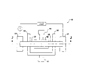
FIG. 1 is a schematic illustrating one embodiment of a MEMS switch having
increased voltage standoff capabilities. FIG. 2 is a cross-sectional view of
the MEMS
switch 10 of FIG. 1 taken across section line 2 as shown. In the illustrated
embodiment, MEMS switch 10 is supported by an underlying substrate 12. The
substrate 12 provides support to the MEMS switch and may represent a rigid
substrate
formed from silicon or germanium for example, or the substrate 12 may
represent a
flexible substrate such as that formed from a polyimide for example. Moreover,
the
substrate 12 may be conductive or may be insulating. In embodiments where the
substrate 12 is conductive, an additional electrical isolation layer (not
shown) may be
included between the substrate 12 and the MEMS switch contacts, anchor and
gate
(described below) to avoid electrical shorting between such components.
The MEMS switch 10 includes a first contact 15 (sometimes referred to as a
source or input contact), a second contact 17 (sometimes referred to as a
drain or
output contact), and a movable actuator 23. In one embodiment, the movable
actuator
23 is conductive and may be formed from any conductive material or alloy. In
one
embodiment, the contacts (15, 17) may be electrically coupled together as part
of a
load circuit and the movable actuator 23 may function to pass electrical
current from
4
CA 02645820 2008-12-04
229968
the first contact 15 to the second contact 17 upon actuation of the switch. As
illustrated in FIG. 2, the movable actuator 23 may include a first actuating
element 21
configured to make an electrical connection with the first contact 15 and a
second
actuating element 22 configured to make an electrical connection with the
second
contact 17. In one embodiment, the first and second actuating elements are
electrically coupled to each other, however, they may nonetheless be
independently
actuated depending upon the attraction force applied to each actuating
element. In
one embodiment, the first and second actuating elements may be simultaneously
attracted toward the substrate 12 during actuation (described further below).
In one
embodiment, the first and second actuating elements are integrally formed as
opposite
ends of actuating elements that share the same anchor region and are
electrically
conductive. In an alternative embodiment, the first and second actuating
elements
may be electrically coupled through additional internal or external electrical
connections. By integrating the first and second actuating elements as part of
the
same movable actuator, external connections may be eliminated thereby reducing
the
overall inductance of the device.
As illustrated in FIG. 1 and FIG. 2, the movable actuator 23 (including the
first actuating element 21 and the second actuating element 22) may be
supported and
mechanically coupled to the substrate 12 by one or more anchors 18. In one
embodiment, the movable actuator 23 may also be electrically coupled to the
anchor(s) 18. In an embodiment where a single anchor 18 is used to support
both the
first actuating element 21 and the second actuating element 22, it may be
desirable for
the anchor 18 to be sufficiently wide (in a direction extending between the
first and
second contacts) such that any strain or inherent stresses associated with one
actuating
element are not transferred or mechanically coupled to the second actuating
element.
Moreover, in an embodiment where a single anchor 18 is used to support both
the first
actuating element 21 and the second actuating element 22, the distance of the
fixed
material between the movable actuating elements may be greater then the
combined
length of the moveable elements.
In accordance with one aspect of the present invention, the MEMS switch 10
includes a common gate 16 controlled by a single gate driver 6 and configured
to
CA 02645820 2008-12-04
229968
contemporaneously impart an attraction force upon both the first and second
actuating
elements 21 and 22. Such attraction force may be embodied as an electrostatic
force,
magnetic force, a piezo-resistive force or as a combination of forces. In an
electrostatically actuated switch, the gate 16 may be electrically referenced
to the
switch reference 14, which in FIG. 1 and FIG. 2 is at the same electrical
potential as
the conduction path of the movable actuator 23. In a magnetically actuated
switch, a
gating signal, such as a voltage, is applied to change the magnetic state of a
material
to provide or eliminate a presence of a magnetic field which drives the
moveable
elements. Similarly, a gating signal such as a voltage can be applied to a
piezoresistive material spanning the moveable elements to induce actuation. In
the
case of both magnetic and piezo-resistive actuation, the gating signal does
not create
an electrostatic attractive force between the moveable elements and therefore
does not
need to be referenced to the moveable elements.
In one embodiment, the gate driver 6 includes a power supply input (not
shown) and a control logic input that provides a means for changing the
actuation
state of the MEMS switch. In one embodiment, the gating voltage is referenced
to the
moveable actuating elements 21 and 22 and the differential voltages between
the two
contacts and respective movable elements are substantially equal. In one
embodiment, the MEMS switch 10 may include a resistive grading network (not
shown) coupled between the contacts and the switch reference 14 to maintain
the
switch reference 14 at a potential that is less than the self-actuation
voltage of the
switch.
By sharing a common gating signal in the MEMS switch 10, a large
actuation voltage that may otherwise surpass the actuation voltage for a
conventional
MEMS switch, would be shared between the first actuating element and the
second
actuating element. For example, in the MEMS switch 10 of FIG. 1 and FIG. 2, if
a
voltage of 200v was placed across the first contact 15 and the second contact
17, and
the switch reference 17 was graded to 100v, the voltage between the first
contact 15
and the first actuating element 21 would be approximately 100v while the
voltage
between the second contact 17 and the second actuating element 22 would also
be
approximately 100v.
6
CA 02645820 2008-12-04
229968
In FIG. 2, the MEMS switch 10 further includes a cap 25 that forms a
hermetic seal with the substrate 12 around the components of MEMS switch 10
including both actuating elements 21 and 22. Typically, many MEMS switches are
formed on a single substrate. These switches are then capped and singulated or
diced.
In one embodiment, the first and second actuating element and the common gate
16 of
MEMS switch 10 are formed and capped on a single die. By including the first
and
second actuating elements within a single cap, it is possible to increase the
standoff
voltage of the MEMS switch without substantially increasing the switch
footprint.
For example, the standoff voltage of the switch effectively can be doubled,
while the
overall switch footprint is only increased slightly more than that of a single
switch.
FIG. 3 is a schematic of a MEMS switch 30 in accordance with another
embodiment of the invention. In the illustrated embodiment, MEMS switch 30 is
substantially similar to MEMS switch 10, however, the movable actuator MEMS
switch 30 further includes an electrical biasing component 39 isolated from
the
conduction path 37 of the movable actuator 23 by an isolation region 36. The
electrical biasing component 39 may represent a conductive layer or trace
formed as
part of the movable actuator in a MEMS photolithographic fabrication process.
In
another embodiment, the electrical biasing component 39 may represent a piezo-
resistive material configured to impart and mechanical force on the movable
actuator
23. In one embodiment, the electrical biasing component 39 may be electrically
referenced to the gate 16. In such an embodiment, the actuation voltage of the
MEMS
switch 30 would be independent of the voltage across the conduction path of
the
movable electrode (e.g., across the first and second contacts) and therefore
can be
increased beyond the normal standoff capabilities of the switch. Although not
shown,
MEMS switch 30 may also be capped as was described with respect to MEMS switch
10.
FIG. 4 is a schematic illustrating one embodiment of a MEMS switch in
which a first actuating element and a second actuating element are physically
separated. As shown, MEMS switch 40 may include a first actuating element 41
supported by a first anchor 48a and a second actuating element 42 supported by
a
second anchor 48b. In an alternative embodiment, the first actuating element
41 and
7
CA 02645820 2008-12-04
229968
the second actuating element 42 may be supported by a single anchor while
maintaining separation between the actuating elements. In the
illustrated
embodiment, the first and the second actuating elements may each include
electrical
biasing components 49 isolated from the conduction path 47 of the respective
actuating element by an isolation region 46. As with MEMS switch 30, the
electrical
biasing component 49 may represent a conductive layer or trace formed as part
of the
actuating element in a MEMS photolithographic fabrication process or a piezo-
resistive material configured to impart and mechanical force on a respective
actuating
element. In one embodiment, the conduction paths 47 of each the actuating
elements
41 and 42 may be electrically coupled by electrical connection 45. Although
not
shown, MEMS switch 40 may also be capped as was described with respect to MEMS
switches 10 and 30.
FIG. 5 is a schematic illustrating an alternative embodiment of a MEMS
switch in which the first actuating element and the second actuating element
are
physically separated. As shown, MEMS switch 50 may include a first actuating
element 51 and a second actuating element 52 supported by a single anchor 58.
As
with the previously described MEMS switches, the first actuating element 51
and the
second actuating element 52 may be commonly actuated to respectively make
electrical contact with contacts 55 and 57 based upon an attraction force
generated by
a signal from the gate 56. As with MEMS switches 10, 30 and 40, MEMS switch 50
may further include a cap 25 which forms a hermetic seal with the substrate 12
over
the various MEMS components.
FIG. 6 is a schematic illustrating an array 60 of two or more MEMS switches
according to one embodiment of the invention. In the illustrated embodiment,
each
MEMS switch 10 includes a movable actuator 23 including a first and a second
actuating element (not shown) that is actuated based upon the actuating state
of
common gate 16. In one embodiment, each MEMS switch 10 in the MEMS switch
array 60 is controlled by a separate gate driver 66. In turn, each gate driver
66
controls the actuation state of the common gate 16 shared between the first
and
second actuating elements of a given MEMS switch 10. In the illustrated
embodiment, the array 60 of two MEMS switches 10 are shown electrically
coupled
8
CA 02645820 2015-10-05
229968
in series with the output contact 17 of a first MEMS switch 10 being connected
to the
input contact 15 of an adjoining MEMS switch 10. However, these or additional
MEMS switches may also be electrically coupled in parallel or series-parallel
combinations depending upon the end-use application. In one embodiment, the
MEMS array 60 may be employed as part of an electrical interruption device
suitable
for arcless interruption of direct current from a current source 61. In order
to achieve
a desirable voltage rating for a particular application such as arcless
current
interruption, the MEMS switches 10 in the MEMS switch array 60 may be
operatively
coupled in series, parallel and series/parallel to achieve the desired voltage
and current
dividing effects.
While there have been described herein what are considered to be preferred
and exemplary embodiments of the present invention, other modifications of
these
embodiments falling within the scope of the invention described herein shall
be
apparent to those skilled in the art.
9