Note : Les descriptions sont présentées dans la langue officielle dans laquelle elles ont été soumises.
CA 02648536 2009-01-07
1
METHODS FOR REMOVING A STABILIZER FROM A METAL
NANOPARTICLE USING A DESTABILIZER
BACKGROUND
[0001] Fabrication of electronic circuit elements using liquid deposition
techniques is of profound interest as such techniques provide potentially low-
cost
alternatives to conventional mainstream amorphous silicon technologies for
electronic
applications such as thin-film transistors (TFTs), light-emitting diodes
(LEDs), RFID
tags, photovoltaics, etc. However the deposition and/or patterning of
functional
electrodes, pixel pads, and conductive traces, lines and tracks which meet the
conductivity, processing, and cost requirements for practical applications
have been a
great challenge.
[0002] Solution-processable conductors are of great interest for printed
electronic applications as electrodes, conducting lines in thin-film
transistors, RFID
tags, photovoltaics, etc. Metal nanoparticle-based inks represent a promising
class of
materials for printed electronics. However, most metal nanoparticles require
large
molecular weight stabilizers to ensure proper solubility and stability. These
large
molecular weight stabilizers inevitably raise the annealing temperatures of
the metal
nanoparticles above 200 C in order to burn off the stabilizers, which
temperatures are
incompatible with most plastic substrates and can cause damage thereto.
[0003] Further, the use of lower molecular weight stabilizers can also be
problematic, as smaller size stabilizers often do not provide desired
solubility and
often fail to effectively prevent coalescence or aggregation of the metal
nanoparticles
before use.
[0004] One of the advantages achieved by embodiments herein is that the
addition of a destabilizer to stabilized metal nanoparticles during or after
the
deposition of the metal nanoparticles interferes with the interaction between
the
stabilizer and the metal nanoparticles or decomposes the stabilizer molecules
into
smaller derivatives. As a result, a stable metal nanoparticle solution for
liquid
deposition is obtained, and also the post-deposition thermal annealing
temperatures
can be much lower due to the removal of the stabilizer following liquid
deposition.
CA 02648536 2009-01-07
2
SUMMARY
[0005] Disclosed generally are a method for forming a conductive feature on
a substrate and a method for manufacturing a thin-film transistor using metal
nanoparticles that are stabilized with a stabilizer, enabling the stabilizer,
destabilizer,
and other reaction by-products to be removed by 1) thermal annealing at a low
temperature, for example, below about 180 C, or 2) washing the substrate with
a
solvent, and thus that can be used to form metal features on a wider range of
substrates.
[0006] In embodiments, the application relates to a method for destabilizing
the stabilizer from a metal nanoparticle. Upon removal of the stabilizer, the
metal
nanoparticle can be used to fabricate conductive elements having sufficiently
high
conductivity for electronic devices by heating at a low temperature, for
example,
below about 180 C, or by washing with a solvent. The metal nanoparticles
prepared
in accordance with the present procedures possess, in embodiments, 1) good
stability
or shelf life and/or 2) low annealing temperatures, and/or 3) good solubility,
and may
be made into metal nanoparticle compositions with suitable liquids, and may be
used
in fabricating liquid-processed conductive elements for electronic devices.
[0007] In embodiments, described is a method of forming conductive
features on a substrate, the method comprising: providing two or more
solutions,
wherein a metal nanoparticle solution contains metal nanoparticles with a
stabilizer
and a destabilizer solution contains a destabilizer that destabilizes the
stabilizer, liquid
depositing the metal nanoparticle solution onto the substrate, wherein during
the
deposition or following the deposition of the metal nanoparticle solution onto
the
substrate, the metal nanoparticles with a stabilizer and the destabilizer are
combined
with each other, destabilizing the stabilizer from the surface of the metal
nanoparticles
with the destabilizer, and removing the stabilizer, destabilizer and reaction
by-
products from the substrate by heating the substrate to a temperature below
about 180
C or by washing with a solvent.
[0008] In further embodiments, described is a method of manufacturing a
thin-film transistor, which comprises a substrate, a gate electrode, a gate
dielectric
layer, a source electrode and a drain electrode and including a semiconductor
layer in
contact with the source/drain electrodes and the gate dielectric layer, the
method
CA 02648536 2012-08-17
3
comprising: providing a substrate with a gate electrode and a gate dielectric
layer,
providing two or more solutions, wherein a metal nanoparticle solution
contains metal
nanoparticles with a stabilizer and a destabilizer solution contains a
destabilizer that
destabilizes the stabilizer, liquid depositing the metal nanoparticle solution
onto the
substrate or gate dielectric layer, wherein during the deposition or following
the
deposition of the metal nanoparticle solution onto the substrate or gate
dielectric layer,
the metal nanoparticle and the destabilizer are combined with each other;
destabilizing
the stabilizer from the surface of the metal nanoparticles with the
destabilizer,
removing the stabilizer, destabilizer and reaction by-products from the
substrate by
heating the substrate to a temperature below about 180 C or washing with a
solvent,
and forming conductive features on the substrate as the gate, source and/or
drain
electrodes.
[0008a] In accordance with another aspect, there is provide a method of
forming conductive features on a substrate, the method comprising:
providing two or more solutions, wherein a metal nanoparticle
solution contains metal nanoparticles with a stabilizer and a destabilizer
solution
contains a destabilizer that destabilizes the stabilizer,
liquid depositing the metal nanoparticle solution onto the substrate,
wherein during the deposition or following the deposition of the metal
nanoparticle
solution onto the substrate, the metal nanoparticles with the stabilizer and
the
destabilizer are combined with each other,
destabilizing the stabilizer from the surface of the metal
nanoparticles with the destabilizer, and
removing the stabilizer and the destabilizer from the substrate by
heating the substrate to a temperature below about 180 C or by washing with a
solvent,
wherein the destabilizing the stabilizer with the destabilizer
decomposes the stabilizer into smaller size stabilizer derivatives.
10008b1 In accordance with a further aspect, there is provide a method of
manufacturing a thin-film transistor, which comprises a substrate, a gate
electrode, a
CA 02648536 2012-08-17
3a
gate dielectric layer, a source electrode and a drain electrode and a
semiconductor
layer in contact with the source/drain electrodes and the gate dielectric
layer, the
method comprising:
providing a substrate with or without a gate electrode and a gate
dielectric layer,
providing two or more solutions, wherein a metal nanoparticle
solution contains metal nanoparticles with a stabilizer and a destabilizer
solution
contains a destabilizer that destabilizes the stabilizer,
liquid depositing the metal nanoparticle solution onto the substrate or
gate dielectric layer to form a gate electrode, source electrode and/or drain
electrode,
wherein during the deposition or following the deposition of the metal
nanoparticle
solution onto the substrate or gate dielectric layer, the metal nanoparticle
and the
destabilizer are combined with each other,
destabilizing the stabilizer from the surface of the metal
nanoparticles with the destabilizer,
removing the stabilizer, destabilizer, and reaction by-products from
the substrate by heating the substrate to a temperature below about 180 C or
washing
with a solvent, and
forming conductive features on the substrate as the gate, source,
and/or drain electrodes.
BRIEF DESCRIPTION OF THE DRAWINGS
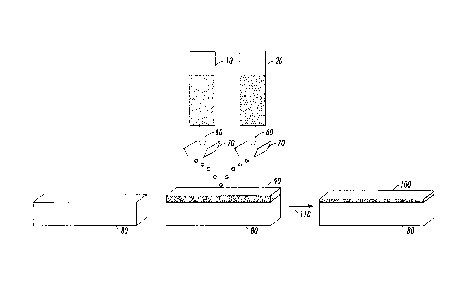
[0009] Figure 1 illustrates an embodiment where the metal solution and
destabilizer solution are transferred to the same or separate printheads by
feed lines
connected to the printhead and simultaneously printed onto the substrate to
form metal
features using an inkjet printer.
100101 Figure 2 illustrates an embodiment where a first solution, either a
metal solution or a destabilizer solution, is printed onto the substrate, and
the second
solution, the other of the two solutions, is thereafter printed consecutively
onto the
first solution, in the same pattern, from the same or different printheads to
form metal
features using an inkjet printer.
CA 02648536 2012-08-17
3b
EMBODIMENTS
[0011] Described is a method of forming conductive features on a substrate
wherein a stabilized metal nanoparticle solution is deposited onto a substrate
and a
destabilizer solution is deposited onto the same substrate to destabilize the
stabilizer.
Destabilizing the stabilizer refers to, for example, any method of weakening
the
interaction or cleaving the connection between the stabilizer and the metal
nanoparticles, including decomposing and/or removing the stabilizer. The
stabilizer
used to stabilize the metal nanoparticles is subsequently removed by heating
at a
temperature below about 180 C, or by washing with a solvent.
[0012] The metal nanoparticle solution herein includes a metal nanoparticle
in a liquid system. In embodiments, the metal nanoparticles are composed of
(i) one
CA 02648536 2009-01-07
4
or more metals or (ii) one or more metal composites. Suitable metals may
include, for
example, Al, Ag, Au, Pt, Pd, Cu, Co, Cr, In, and Ni, particularly the
transition metals,
for example, Ag, Au, Pt, Pd, Cu, Cr, Ni, and mixtures thereof. Silver may be
used as
a suitable metal. Suitable metal composites may include Au-Ag, Ag-Cu and Au-Ag-
Pd. The metal composites may include non-metals, such as, for example, Si, C,
0, S,
Se, P, and Ge. The various components of the metal composite may be present in
an
amount ranging for example from about 0.01% to about 99.9% by weight,
particularly
from about 10% to about 90% by weight. In embodiments, the metal composite is
a
metal alloy composed of silver and one, two or more other metals, with silver
comprising for example at least about 20% of the nanoparticles by weight,
particularly
greater than about 50% of the nanoparticles by weight. Unless otherwise noted,
the
weight percentages recited herein for the components of the metal
nanoparticles do
not include the stabilizer.
[0013] The term "nano" as used in "metal nanoparticles" refers to, for
example, a particle size of less than about 1,000 nanometers (nm), such as
from about
0.5 nm to about 1,000 nm, for example, from about 1 nm to about 800 nm, from
about
1 nm to about 500 nm, from about 1 nm to about 100 nm or from about 1 nm to
about
20 nm. The particle size refers to the average diameter of the metal
particles, as
determined by TEM (transmission electron microscopy) or other suitable method.
[0014] As the liquid system, any suitable liquid or solvent may be used for
the metal nanoparticle solution, including, for example, organic solvents and
water.
The volume of the solvent in the metal nanoparticle solution is, for example,
from
about 10 weight percent to about 98 weight percent, from about 50 weight
percent to
about 90 weight percent and from about 60 weight percent to about 85 weight
percent.
For example, the liquid solvent may comprise water, an alcohol such as, for
example,
methanol, ethanol, propanol, butanol, pentanol, hexanol, heptanol, octanol or
combinations thereof; a hydrocarbon such as, for example, pentane, hexane,
cyclohexane, heptane, octane, nonane, decane, undecane, dodecane, tridecane,
tetradecane, toluene, benzene, xylene, mesitylene, tetrahydrofuran;
chlorobenzene;
dichlorobenzene; trichlorobenzene; nitrobenzene; cyanobenzene; acetonitrile;
or
combinations thereof.
[0015] One, two, three or more solvents may be used in the metal
nanoparticle solution. In embodiments where two or more solvents are used,
each
CA 02648536 2009-01-07
solvent may be present at any suitable volume ratio or molar ratio such as for
example
from about 99(first solvent):1(second solvent) to about 1(first
solvent):99(second
solvent).
[0016] The concentration of metal in the metal nanoparticle solution may be,
for example, from about 2 weight percent to about 90 weight percent, from
about 5
weight percent to about 80 weight percent, from about 10 weight percent to
about 60
weight percent, or from about 15 weight percent to about 50 weight percent, of
the
metal nanoparticle solution.
[0017] The stabilizer preferentially associates with the external surface of
the metal nanoparticles. By doing so, the metal nanoparticles are able to
remain
sufficiently stable in a dispersed solution, that is, remain suspended in the
solution in a
substantially homogeneously distributed manner, for a time period where there
is
minimal precipitation or aggregation of the nanoparticles such as, for
example, at least
about 3 hours, or from about 3 hours to about 1 month, from about 1 day to
about 3
months, from about 1 day to about 6 months, from about 1 week to over 1 year,
prior
to liquid deposition. In this way, when liquid deposited, good conductive
features
may be formed on the substrate.
[0018] The stabilizer on the surface of the metal nanoparticles can be any
suitable compound such as a compound comprising a moiety selected from the
group
consisting of ¨NH2 such as butylamine, pentylamine, hexylamine, heptylamine,
octylamine, nonylamine, decylamine, undecylamine, dodecylamine, tridecylamine,
tetradecylamine, pentadecylamine, hexadecylamine, oleylamine, octadecylamine,
diaminopentane, diaminohexane, diaminoheptane, diaminooctane, diaminononane,
diaminodecane, diaminooctane, ¨NH¨ such as dipropylamine, dibutylamine,
dipentylamine, dihexylamine, diheptylamine, dioctylamine, dinonylamine,
didecylamine, methylpropylamine, ethylpropylamine, propylbutylamine,
ethylbutylamine, ethylpentylamine, propylpentylamine, butylpentylamine,
polyethyleneimine, an ammonium salt such as tributylammonium bromide,
didodecyldimethylammonium bromide, benzyltriethylammonium chloride, ¨SH
such as butanethiol, pentanethiol, hexanethiol, heptanethiol, octanethiol,
nonanethiol,
decanethiol, undecanethiol, dodecanethiol, ¨S02M (M is NH4+, Lit, Nat, K+, or
Cs)
such as sodium octylsulfate, sodium dodecylsulfate, ¨OH (alcohol) such as
terpinol,
starch, glucose, poly(vinyl alcohol), ¨05H4N (pyridyl) such as
poly(vinylpyridine),
CA 02648536 2009-01-07
6
poly(vinylpyridine-co-styrene), poly(vinylpyridine-co-butyl methacrylate),
¨C(=0)0H such as butyric acid, pentanoic acid, hexanoic acid, heptanoic acid,
octanoic acid, nonanoic acid, decanoic acid, undecanoic acid, dodecanoic acid,
tridecanoic acid, myristic acid, pentadecanoic acid, palmitic acid,
heptadecanoic acid,
stearic acid, oleic acid, nonadecanoic acid, icosanoic acid, eicosenoic acid,
elaidic
acid, linoleic acid, pamitoleic acid, poly(acrylic acid), ¨0C(=S)SH (xanthic
acid),
such as 0-methylxanthate, 0-ethylxanthate, 0-propylxanthic acid, 0-
butylxanthic
acid, 0-pentylxanthic acid, 0-hexylxanthic acid, 0-heptylxanthic acid, 0-
octylxanthic
acid, 0-nonylxanthic acid, 0-decylxanthic acid, 0-undecylxanthic acid, 0-
dodecylxanthic acid, and R'R' P¨ and R'R"P(=0)¨. R' and R" are hydrocarbon
groups. Examples of R'R' P¨ and R'R' P(=0)¨ may include trioctylphosphine and
trioctylphosphine oxide, or a combination thereof.
100191 Unless otherwise indicated, in identifying the substituents for R, R'
and R" the phrase "hydrocarbon group" encompasses both unsubstituted
hydrocarbon
groups and substituted hydrocarbon groups. Unsubstituted hydrocarbon groups
may
include any suitable substituent such as, for example, a straight chain or
branched
alkyl group, a cycloalkyl group, an aryl group, an alkylaryl group, arylalkyl
group or
combinations thereof. Alkyl and cycloalkyl substituents may contain from about
1 to
about 30 carbon atoms, from about 5 to 25 carbon atoms and from about 10 to 20
carbon atoms. Examples of alkyl and cycloalkyl substituents include, for
example,
methyl, ethyl, propyl, butyl, pentyl, hexyl, heptyl, octyl, nonyl, decyl,
undecyl,
dodecyl, tridecyl, tetradecyl, pentadecyl, hexadecyl, heptadecyl, octadecyl,
nonadecyl,
or eicosanyl, and combinations thereof. Aryl groups substituents may contain
from
about 6 to about 48 carbon atoms, from about 6 to about 36 carbon atoms, from
about
6 to about 24 carbon atoms. Examples of aryl substituents include, for
example,
phenyl, methylphenyl (tolyl), ethylphenyl, propylphenyl, butylphenyl,
pentylphenyl,
hexylphenyl, heptylphenyl, octylphenyl, nonylphenyl, decylphenyl,
undecylphenyl,
dodecylphenyl, tridecylphenyl, tetradecylphenyl, pentadecylphenyl,
hexadecylphenyl,
heptadecylphenyl, octadecylphenyl, or combinations thereof. Substituted
hydrocarbon
groups may be the unsubstituted hydrocarbon groups described herein which are
substituted with one, two or more times with, for example, a halogen
(chlorine,
fluorine, bromine and iodine), a nitro group, a cyano group, an alkoxy group
(methoxy, ethoxy and propoxy), or heteroaryls. Examples of heteroaryls groups
may
CA 02648536 2009-01-07
7
include thienyl, furanyl, pyridinyl, oxazoyl, pyrroyl, triazinyl, imidazoyl,
pyrimidinyl,
pyrazinyl, oxadiazoyl, pyrazoyl, triazoyl, thiazoyl, thiadiazoyl, quinolinyl,
quinazolinyl, naphthyridinyl, carbazoyl, or combinations thereof
[0020] Thus, in embodiments is described a method of forming conductive
features on a substrate, wherein the stabilized metal nanoparticle is combined
with a
destabilizer that destabilizes the stabilizer from the surface of metal
nanoparticle. The
destabilizer, stabilizer and any reaction by-products may be removed by
heating at a
temperature below about 180 C, or by washing with a solvent.
[0021] The stabilizer as used herein and further described in embodiments
are those stabilizers that may be removed or that can form reaction by-
products that
may be removed by heating the metal nanoparticle to a temperature less than
about
180 C or by washing with a solvent with the addition of an additional
destabilizer
that interacts with or decomposes the stabilizer.
[0022] The amount of the stabilizer in the metal nanoparticle may be, for
example, from about 1 weight percent to about 80 weight percent, from about 2
weight percent to about 60 weight percent, from about 5 weight percent to
about 50
weight percent, or from about 10 weight percent to about 40 weight percent.
[0023] The stabilizer may be destabilized by combining the metal
nanoparticle with a destabilizer during or following the deposition of the
metal
nanoparticle solution onto a substrate. The term "destabilize" as used herein
refers to,
for example, either 1) cleaving the stabilizer from its association with the
surface of
the metal nanoparticles or 2) decomposing of the stabilizer into smaller sized
derivatives. Decomposition in this regard thus refers to, for example, a
reduction of
the size of the stabilizer, for example, by shortening the chain length of
carbon chains
therein. The decomposition results in derivatives that may or may not be
stabilizers
and that have lower molecular weights than the initial stabilizer.
[0024] In embodiments, the destabilizer in the destabilizer solution interacts
with the stabilizer to disassociate the stabilizer from the surface of the
metal
nanoparticles. As used herein, the term "destabilizer" refers to any compound
or
composition that interacts with the stabilizer on the surface of the
nanoparticles,
resulting in the destabilization or facilitating the destabilization of
stabilizer
compound from the surface of the metal nanoparticles.
CA 02648536 2009-01-07
8
[0025] In embodiments, the stabilizer is physically or chemically associated
with the surface of the metal nanoparticles. In this way, the nanoparticles
have the
stabilizer thereon outside of a liquid system. That is, the nanoparticles with
the
stabilizer thereon, may be isolated and recovered from the reaction mixture
solution
used in forming the nanoparticles.
[0026] As used herein, the phrase "physically or chemically associated"
between the metal nanoparticles and the stabilizer can be a chemical bond
and/or other
physical attachment. The chemical bond can take the form of, for example,
covalent
bonding, hydrogen bonding, coordination complex bonding, or ionic bonding, or
a
mixture of different chemical bonds. The physical attachment can take the form
of,
for example, van der Waals' forces or dipole-dipole interaction, or a mixture
of
different physical attachments. The destabilization of the stabilizer from the
metal
nanoparticles occurs through the use of a destabilizer and thus the
stabilizer,
destabilizer and other reaction by-products can be removed from the metal
nanoparticles (1) by heating at a temperature below about 180 C, or (2) by
washing
with a solvent.
[0027] In embodiments, the type of the destabilizer is specific to the type of
stabilizer used and can be a stabilizer itself to the metal nanoparticles. The
destabilizer may also have stronger interactions than the stabilizer to the
surface of the
metal nanoparticles, but the destabilizer, in taking the place of the
stabilizer on the
surface of the metal nanoparticles, can be removed by heating the metal
nanoparticle
to a temperature below about 180 C, or by washing with a solvent.
[0028] In embodiments, the destabilizer in the destabilizer solution can be a
reactant to the stabilizers. For example, organoamine-stabilized metal
nanoparticles
can be destabilized with an acid as a destabilizer such as, for example, a
saturated
aliphatic acid, unsaturated aliphatic acid, saturated aliphatic dicarboxylic
acid,
unsaturated aliphatic dicarboxylic acid, aromatic carboxylic acid, hydroxy
carboxylic
acid, methoxy carboxylic acid, carboxylic acid with a substituent or a
hydrocarbon
group, inorganic acid such as HC1, HBr, HNO3, or mixtures thereof. As used
herein,
the term "organoamine" includes all amines substituted with one or more
hydrocarbon
groups. The acid or by-products of the acid and the organoamine can be removed
by
heating at a temperature below about 180 C, or by washing with a solvent. The
acid
CA 02648536 2009-01-07
9
reacts with the amine groups and thus forms the acid-organoamine complex that
may
or may not remain on the surface of the metal nanoparticles.
[0029] If a large excess of acid is used such as, for example, a short chain
(from about 3 to 14 carbon atoms) carboxylic acid, most of the surface of the
metal
nanoparticles remain covered with carboxylic acid as the carboxylic acid has
stronger
interaction with the metal nanoparticles. The acid and the by-products of the
acid-
organoamine complex can be removed by heating at a temperature below about
180 C, or by washing with a solvent such as water, an alcohol, or a
hydrocarbon.
[0030] If a larger chain carboxylic acid such as oleic acid is used, a short
chain organothiol such as, for example, butanethiol, pentanethiol,
hexanethiol,
heptanethiol, octanethiol or combination thereof can be used as a
destabilizer. As
used herein, the term "organothiol" includes all thiols substituted with one
or more
hydrocarbon groups. An organothiol has a stronger interaction with the metal
nanoparticles than a larger chain carboxylic acid and can replace the
carboxylic acid
on the surface of the metal nanoparticles. Thus, a metal nanoparticle
stabilized with a
short chain organothiol stabilizer can then be annealed at a temperature below
about
180 C to remove the organothiol stabilizer.
[0031] In embodiments, the destabilizer in the destabilizer solution can be a
catalyst to facilitate the decomposition of the stabilizers. For example,
ether or ester-
containing stabilizers can undergo chain cleavage in the presence of an acid
such as,
for example, HC1, HBr, HNO3 or H2SO4. Ether containing stabilizers may be
represented by the formula R(OCH2CH2)nX where R is hydrogen or any suitable
hydrocarbon group, n is the number of repeating units from about 1 to about
50, from
about 2 to about 40 and from about 4 to about 25 and X is a functional group
that
stabilizes the metal nanoparticles and may be such as, for example, ¨NH2,
¨NH¨,
¨SH, ¨S02M (wherein M may be NH4+, Lit, Nat, K+, or Cs) ¨OH, ¨05H4N,
¨C(=0)0H, ¨0C(=S)SH (xanthic acid), R'R"P¨, R'R' P(=0)¨ or combinations
thereof. R' and R" are a hydrocarbon group.
[0032] Ester containing stabilizers may be represented by, for example, the
formula RC(=0)OR'X or XR'C(=0)OR where R is hydrogen, or any suitable
hydrocarbon group; R' is any suitable divalent moiety such as, for example,
¨CH2¨, ¨
CH2CH2¨, ¨CH2CH2CH2¨, ¨CH2CH2CH2CH2, phenylene, thienylene, or
combinations thereof; and X is a functional group that stabilizes the metal
CA 02648536 2009-01-07
nanoparticles such as, for example, ¨NH2, ¨NH¨, ¨SH, ¨S02M , wherein M is
NH4+, Lit, Nat, K+, or Cs, ¨OH, ¨05H4N, ¨C(=0)0H, ¨0C(=S)SH (xanthic
acid), R'R"P¨, R'R' P(=0)¨ , or combinations thereof, and wherein R' and R"
are
a hydrocarbon group. Further, the ether or ester-containing stabilizer can be
a
polymer that can form low molecular weight by-products in the presence of an
acid
destabilizer and the low molecular weight by-products can be removed by
heating at a
temperature below about 180 C, or by washing with a solvent.
[0033] As the liquid system, any suitable liquid or solvent used for the metal
nanoparticle solution may also be used for the destabilizer solution, and the
liquid or
solvent used for the destabilizer solution may be the same or different liquid
or
solvent from the metal nanoparticle solution.
[0034] The concentration of the destabilizer in the destabilizer solution may
be, for example, from about 1 weight percent to about 100 weight percent, from
about
5 weight percent to about 80 weight percent, from about 10 weight percent to
about 60
weight percent, or from about 20 weight percent to about 50 weight percent.
[0035] The fabrication of an electrically conductive element from a
stabilized metal nanoparticle solution and a destabilizer solution can be
carried out by
depositing the stabilized metal nanoparticle solution and the destabilizer
solution on a
substrate using any liquid deposition technique at any suitable time prior to
or
subsequent to the formation of other optional layer or layers on the
substrate. Thus,
liquid deposition of the stabilized metal nanoparticle solution and the
destabilizer
solution on the substrate can occur either on a substrate or on a substrate
already
containing layered material, for example, a semiconductor layer and/or an
insulating
layer.
[0036] The phrases "liquid deposition technique" or "liquid depositing" refer
to, for example, the deposition of a stabilized metal nanoparticle solution
and a
destabilizer solution using a liquid process such as liquid coating or
printing. The
stabilized metal nanoparticle solution and the destabilizer solution may be
referred to
as inks when printing is used. Examples of liquid coating processes may
include, for
example, spin coating, blade coating, rod coating, dip coating, and the like.
Examples
of printing techniques may include, for example, lithography or offset
printing,
gravure, flexography, screen printing, stencil printing, inkjet printing,
stamping (such
as microcontact printing), and the like. Liquid deposition deposits a layer
comprising
CA 02648536 2009-01-07
11
of the stabilized metal nanoparticle and the destabilizer having a thickness
ranging
from about 5 nanometers to about 5 micrometers, preferably from about 10
nanometers to about 1000 nanometers, which, at this stage, may or may not
exhibit
appreciable electrical conductivity.
[0037] In embodiments, liquid deposition can be implemented by using an
inkjet printer, which has two or more reservoirs, a first reservoir containing
a metal
nanoparticle solution such as silver nanoparticles, and a second reservoir
containing a
destabilizer solution, with other optional components being present in the
first, second
and/or additional reservoirs. Printing may be effected from the reservoirs
simultaneously or consecutively through one or more print heads onto a
substrate.
The metal nanoparticle and the destabilizer combine during or after printing
on the
substrate to destabilize the stabilizer.
[0038] In embodiments, the metal nanoparticle solution and the destabilizer
solution are transferred to the same or separate printheads and combined
during the
printing of both the metal nanoparticle solution and the destabilizer solution
onto the
substrate. As used herein, "during printing" refers to, for example, the metal
nanoparticle solution and the destabilizer solution being printed
simultaneously onto
the substrate from the same or different printheads, and thus that the
respective
solutions effectively combine during printing onto the substrate, even though
the bulk
of the destabilization (interaction between the destabilizer and the
stabilizer) may
occur following printing onto the substrate.
[0039] As a way of illustrating this embodiment, Figure 1, for convenience,
displays the metal nanoparticle solution and destabilizer solution being
printed by
separate printheads using an inkjet printer. In Figure 1, the metal
nanoparticle
solution (10) and destabilizer solution (20) are transferred to separate
printheads (70)
by feed lines (60) connected to the printheads (70). Both solutions are
simultaneously
printed onto the substrate (80) to form features comprising of metal
nanoparticles
(90). A conductive metal film (100) is then formed with thermal annealing
(110).
[0040] In embodiments, the metal nanoparticle solution and the destabilizer
solution are combined on the substrate after first printing one of the
solutions and
thereafter subsequently printing the second solution onto the first printed
solution. As
used herein, "after printing" refers to, for example, the metal nanoparticle
solution and
CA 02648536 2009-01-07
12
the destabilizer solution being printed consecutively onto the substrate from
the same
or different printheads.
[0041] As a way of illustrating this embodiment, Figure 2, for convenience,
displays the metal nanoparticle solution and destabilizer solution being
printed by
separate printheads using an inkjet printer. In Figure 2, the metal
nanoparticle
solution (10) is transferred to the printhead (70) by a feed line (60) and
printed onto
the substrate (80). The destabilizer solution (20) is subsequently transferred
to its
printhead (70) by a feed line (60) and printed consecutively onto the
substrate (80)
with the previously printed metal nanoparticles to form features comprising of
metal
nanoparticles (90). A conductive metal film (100) is then formed with thermal
annealing (110).
[0042] In embodiments, the stabilized metal nanoparticles solution and the
destabilizer solution can be spin-coated, for example, for about 10 seconds to
about
1000 seconds, for about 50 seconds to about 500 seconds or from about 100
seconds
to about 150 seconds, onto a substrate at a speed, for example, from about 100
revolutions per minute ("rpm") to about 5000 rpm, from about 500 rpm to about
3000
rpm and from about 500 rpm to about 2000 rpm.
[0043] The substrate may be composed of, for example, silicon, glass plate,
plastic film or sheet. For structurally flexible devices, a plastic substrate,
such as, for
example, polyester, polycarbonate, polyimide sheets and the like may be used.
The
thickness of the substrate may be from amount 10 micrometers to about 10
millimeters, from about 50 micrometers to about 2 millimeters, especially for
a
flexible plastic substrate and from about 0.4 millimeters to about 10
millimeters for a
rigid substrate such as glass or silicon.
[0044] In embodiments, the destabilizer, stabilizer and any residual solvents
or reaction by-products may be removed by heating the deposited metal
nanoparticle
and the destabilizer to a temperature of, for example, below about 180 C, at
or below
about 170 C, or at or about below 150 C, 1) to remove the stabilizer, the
destabilizer, reaction by-products, and any residual solvents, and 2) to
induce the
metal nanoparticles to form an electrically conductive layer, which is
suitable for use
as an electrically conductive element in electronic devices. The heating
temperature is
one that does not cause adverse changes in the properties of previously
deposited
layer(s) or the substrate (whether single layer substrate or multilayer
substrate). Also,
CA 02648536 2009-01-07
13
the low heating temperatures described above allow the use of plastic
substrates,
which may not withstand annealing temperature above about 200 C.
[0045] In embodiments, the destabilizer, stabilizer, reaction by-products, and
any residual solvents may also be removed by washing the deposited composition
of
the metal nanoparticles with a solvent. For example, the solvent may comprise,
for
example, water, hydrocarbon solvents such as pentane, hexane, cyclohexane,
heptane,
octane, nonane, decane, undecane, dodecane, tridecane, tetradecane, toluene,
xylene,
mesitylene, methanol, ethanol, propanol, butanol, pentanol, hexanol, heptanol,
octanol, tetrahydrofuran, chlorobenzene, dichlorobenzene, trichlorobenzene,
nitrobenzene, cyanobenzene, acetonitrile, dichloromethane, N,N-
dimethylformamide
(DMF) and combinations thereof.
[0046] The heating can be performed for a time ranging from, for example,
about 1 second to about 10 hours and from about 10 seconds to about 1 hour.
The
heating can be performed in air, in an inert atmosphere, for example, under
nitrogen or
argon, or in a reducing atmosphere, for example, under nitrogen containing
from
about 1 to about 20 percent by volume hydrogen. The heating can also be
performed
under normal atmospheric conditions or at a reduced pressure of, for example,
from
1000 mbars to about 0.01 mbars.
[0047] As used herein, the term "heating" encompasses any technique(s) that
can impart sufficient energy to the heated material to cause the desired
result such as
thermal heating (for example, a hot plate, an oven, and a burner), infra-red
("IR")
radiation, microwave radiation, heating by a laser beam, or UV radiation, or a
combination thereof.
[0048] Heating produces a number of effects. Prior to heating, the layer of
the deposited metal nanoparticles may be electrically insulating or with very
low
electrical conductivity, but heating results in an electrically conductive
layer
composed of annealed metal nanoparticles, which increases the conductivity. In
embodiments, the annealed metal nanoparticles may be coalesced or partially
coalesced metal nanoparticles. In embodiments, it may be possible that in the
annealed metal nanoparticles, the metal nanoparticles achieve sufficient
particle-to-
particle contact to form the electrically conductive layer without
coalescence.
CA 02648536 2009-01-07
14
[0049] In embodiments, after heating, the resulting electrically conductive
layer has a thickness ranging, for example, from about 5 nanometers to about 5
micrometers and from about 10 nanometers to about 1000 nanometers.
[0050] The resulting conductive elements can be used as electrodes,
conductive pads, thin-film transistors, conductive lines, conductive tracks,
and the like
in electronic devices such as thin-film transistors, organic light emitting
diodes, RFID
(radio frequency identification) tags, photovoltaic, and other electronic
devices which
require conductive elements or components.
[0051] The conductivity of the resulting metal element produced by heating
the deposited metal nanoparticle composition is, for example, more than about
100
Siemens/centimeter ("S/cm"), more than about 1000 S/cm, more than about 2,000
S/cm, more than about 5,000 S/cm, more than about 10,000 S/cm.
[0052] In yet other embodiments, there is provided a thin film transistor
comprising:
(a) an dielectric layer;
(b) a gate electrode;
(c) a semiconductor layer;
(d) a source electrode;
(e) a drain electrode, and
(f) a substrate
wherein the dielectric layer, the gate electrode, the semiconductor layer, the
source electrode, the drain electrode and the substrate are in any sequence as
long as
the gate electrode and the semiconductor layer both contact the insulating
dielectric
layer, and the source electrode and the drain electrode both contact the
semiconductor
layer, and, the semiconductor layer is comprised of an organic, inorganic, or
an
organic/inorganic hybrid semiconductor compound.
[0053] In embodiments and with further reference to the present disclosure,
the substrate layer may generally be a silicon material inclusive of various
appropriate
forms of silicon, a metal film or sheet, a glass plate, a plastic film or a
sheet, a paper, a
fabric, and the like depending on the intended applications. For structurally
flexible
devices, a metal film or sheet such as, for example, aluminum, a plastic
substrate,
such as, for example, polyester, polycarbonate, polyimide sheets, and the
like, may be
selected. The thickness of the substrate may be, for example, from about 10
CA 02648536 2012-08-17
micrometers to over 10 millimeters with a specific thickness being from about
50
micrometers to about 10 millimeters, especially for a flexible plastic
substrate, and
from about 0.5 to about 10 millimeters.
[0054] The insulating dielectric layer, which can separate the gate electrode
from the source and drain electrodes, and in contact with the semiconductor
layer, can
generally be an inorganic material film, an organic polymer film, or an
organic-
inorganic composite film. Examples of inorganic materials suitable as the
dielectric
layer may include silicon oxide, silicon nitride, aluminum oxide, barium
titanate,
barium zirconate titanate, and the like. Examples of organic polymers for the
dielectric layer may include polyesters, polycarbonates, poly(vinyl phenol),
polyimides, polystyrene, poly(methacrylate)s, poly(acrylate)s, epoxy resin,
and the
like. Examples of inorganic-organic composite materials may include spin-on
glass
such as pMSSQ (polymethylsilsesquioxane), metal oxide nanoparticles dispersed
in
polymers, such as polyester, polyimide, epoxy resin, and the like. The
thickness of the
dielectric layer can be, for example, from about 1 nanometer to about 5
micrometer
with a more specific thickness being about 10 nanometers to about 1000
nanometers.
More specifically, the dielectric material has a dielectric constant of, for
example, at
least about 3, thus a suitable dielectric thickness of about 300 nanometers
can provide
a desirable capacitance, for example, of about 10-9 to about 10-7 F/cm2.
[0055] Situated, for example, between and in contact with the dielectric
layer and the source/drain electrodes is the active semiconductor layer
comprised of
semiconductors, and wherein the thickness of this layer is generally, for
example,
about 10 nanometers to about 1 micrometer, or about 40 to about 100
nanometers.
This layer can generally be fabricated by solution processes such as spin
coating,
casting, screen, stamp, or jet printing of a solution of semiconductors.
[0056] The gate electrode can be a thin metal film, a conducting polymer
film, a conducting film generated from a conducting ink or paste, or the
substrate
itself (for example heavily doped silicon). Examples of the gate electrode
materials
may include gold, chromium, indium tin oxide, conducting polymers, such as
polystyrene sulfonate-doped poly(3,4-ethylenedioxythiophene) (PSS/PEDOT), a
conducting ink/paste comprised of carbon black/graphite or colloidal silver
dispersion
contained in a polymer binder, such as ElectrodagTM available from Acheson
Colloids
Company, and silver filled electrically conductive thermoplastic ink available
from
CA 02648536 2009-01-07
16
Noelle Industries, and the like. The gate layer may be prepared by vacuum
evaporation, sputtering of metals or conductive metal oxides, coating from
conducting
polymer solutions or conducting inks, or dispersions by spin coating, casting
or
printing. The thickness of the gate electrode layer may be, for example, from
about 10
nanometers to about 10 micrometers, and a specific thickness is, for example,
from
about 10 to about 1000 nanometers for metal films, and about 100 nanometers to
about 10 micrometers for polymer conductors.
[0057] The source and drain electrode layer can be fabricated from materials
which provide a low resistance ohmic contact to the semiconductor layer.
Typical
materials suitable for use as source and drain electrodes may include those of
the gate
electrode materials such as silver, gold, nickel, aluminum, platinum,
conducting
polymers, and conducting inks. Typical thickness of this layer may be, for
example,
from about 40 nanometers to about 1 micrometer with the more specific
thickness
being about 100 to about 400 nanometers. The TFT devices contain a
semiconductor
channel with a width W and length L. The semiconductor channel width may be,
for
example, from about 10 micrometers to about 5 millimeters with a specific
channel
width being about 100 micrometers to about 1 millimeter. The semiconductor
channel length may be, for example, from about 1 micrometer to about 1
millimeter
with a more specific channel length being from about 5 micrometers to about
100
micrometers.
[0058] In embodiments, at least one of the gate, source or drain electrode in
a thin-film transistor is formed by using a method described herein to form
conductive
features on a substrate, the method comprising: providing two or more
solutions,
wherein a metal nanoparticle solution contains metal nanoparticles with a
stabilizer
and a destabilizer solution contains a destabilizer that interacts with the
stabilizer;
liquid depositing the metal nanoparticle solution onto the substrate, wherein
during
the deposition or following the deposition of the metal nanoparticle solution
onto the
substrate, the metal nanoparticle solution and the destabilizer solution are
combined
each other; destabilizing the stabilizer from the surface of the metal
nanoparticles with
the destabilizer and removing the stabilizer, destabilizer and reaction by-
products by
heating the substrate to a temperature below about 180 C, or by washing with
a
solvent, to form conductive features on the substrate.
CA 02648536 2009-01-07
17
[0059] Other known suitable materials not recited herein for the various
components of the TFT devices of the present disclosure can also be selected
in
embodiments.
[0060] EXAMPLE
[0061] Synthesis of oleic acid-stabilized silver nanoparticles
[0062] a. Synthesis of oleylamine-stabilized silver nanoparticles
[0063] Silver acetate (3.34 g, 20 mmol) and oleylamine (13.4 g, 50 mmol)
are dissolved in 40 mL toluene and stirred at 55 C for 5 minutes.
Phenylhydrazine
(1.19 g, 11 mmol) solution in toluene (10 mL) is added into above solution
drop-wise
with vigorous stirring and stirred at 55 C for 10 additional minutes. The
resulting
solution forms a precipitate when added drop-wise to a mixture of
acetone/methanol
(150 mL/150 mL). The precipitate is subsequently filtered and washed briefly
with
acetone and methanol yielding a gray solid of oleylamine-stabilized silver
nanoparticles.
[0064] b. Synthesis of oleic acid-stabilized silver nanoparticles
[0065] The oleylamine acid-stabilized nanoparticles are dissolved in
50 mL of hexane and subsequently added drop-wise to a solution of oleic acid
(14.12
g, 50 mmol) in hexane (50 mL) at room temperature. After 30 minutes, hexane is
removed and the residue poured into a solution of stirring methanol (200 mL).
After
filtration, washing with methanol and drying (in vacuo), a gray solid is
obtained. The
yield was 3.05 grams (96%, based on Ag content of 68 % from TGA analysis).
[0066] Preparation of Silver Nanoparticles Solution (Dispersion)
100671 The oleic acid-stabilized silver nanoparticles are dissolved in toluene
to form a dispersed homogeneous solution. The concentration of silver
nanoparticles
is 15 weight percent. Next, the dispersed solution is filtered using a 0.2
micron PTFE
(polytetrafluoroethylene, Teflon) or glass filter.
[0068] Preparation of destabilizer solution using 1-butanethiol as a
destabilizer
[0069] A 15 weight percent solution of 1-butanethiol is prepared by
dissolving 1-butanethiol in toluene and filtered using a 0.2 micron PTFE or
glass
filter.
CA 02648536 2013-08-23
18
100701 Printing on a Substrate and Annealing to Form Conductive Silver
Patterns
100711 The solution of oleic acid-stabilized silver nanoparticles and
1-butanethiol solution are placed into two separated cartridges of an inkjet
printer and
printed in a designed pattern onto a glass substrate by first printing the
oleic acid-
stabilized silver nanoparticle solution onto the substrate and then printing
1-butanethiol solution directly on top of the pattern where oleic acid-
stabilized silver
nanoparticle solution was printed. The glass substrate is then heated on a
hotplate to a
temperature of 140 C for 30 minutes and cooled. Inspection confirms the
formation
of conductive silver patterns on the surface of the glass substrate.
[0072] It will be appreciated that various of the above-disclosed and other
features and functions, or alternatives thereof, may be desirably combined
into many
other different systems or applications. Also, various alternatives and
modifications,
or improvements therein may be subsequently made by those skilled in the art,
and are
also intended to be within the scope of the invention.