Note : Les descriptions sont présentées dans la langue officielle dans laquelle elles ont été soumises.
CA 02649289 2009-01-12
MICRO-ELECTRO-DISCHARGE MACHINING METHODS AND APPARATUS
Technical Field
[0001] The invention relates to machining and, in particular to electro-
discharge
machining, also known as EDM.
Back rg ound
[0002] Electro-discharge machining (EDM) is a technology that may be applied
to
machining electrically-conductive materials. In EDM, an electrode immersed in
a
dielectric fluid is brought near to a surface of a workpiece. An electrical
potential is
applied between the electrode and the workpiece. The electrical potential
results in the
release of energy by way of an electrical discharge between the electrode and
the
workpiece. The discharge causes some material to be removed from the
workpiece.
[0003] EDM techniques can be used to machine hard materials that are otherwise
difficult to machine. EDM techniques can be very precise. A modern EDM machine
typically has a numerically controlled (NC) position controller connected to
control the
position of an electrode relative to a workpiece. The electrode may be
advanced to cut
into the workpiece.
[0004] EDM techniques may be applied on a small scale. Micro-electro-discharge
machining ( EDM) involves erosion of a workpiece by small spark discharge
pulses
generated between a microscopic electrode tip and a workpiece in a dielectric
fluid.
EDM is described in:
= T. Masaki, K. Kawata, T. Masuzawa, Micro Electro-Discharge Machining and its
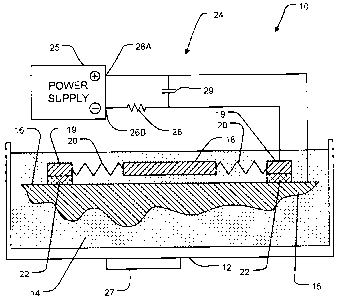
Applications, Proc. IEEE MEMS, 1990, pp. 21-26;
= L.L. Chu, K. Takahata, P. Selvaganapathy, Y.B. Gianchandani, J.L. Shohet, A
Micromachined Kelvin Probe with Integrated Actuator for Microfluidic and
Solid-State Applications, J. MEMS, 14(4), 2005, pp. 691-698; and,
CA 02649289 2009-01-12
-2-
K. Takahata, Y.B. Gianchandani, Bulk-Metal-Based MEMS Fabricated by
Micro-Electro-Discharge Machining, Proc. IEEE Canadian Conf. Electr. Comput.
Eng. (CCECE), 2007, pp. 1-4.
[0005] Some EDM techniques that are described in the literature involve a
serial
process that uses a single electrode tip in conjunction with numerical control
(NC) of the
tip and the workpiece to produce features of structure individually. The
throughput of
such techniques is inherently low. Batch-mode EDM that uses arrays of
high-aspect-ratio microelectrodes may achieve high parallelism and increased
throughput.
[0006] A batch-mode EDM process is described in: K. Takahata, Y.B.
Gianchandani,
Batch Mode Micro-Electro- Discharge Machining J. MEMS, 11(2), 2002, pp.102-
110.
This paper describes arrays of EDM electrodes fabricated using a LIGA
process. The
arrays of electrodes were advanced into the workpiece using the vertical NC
stage in an
EDM apparatus. Making electrode arrays by the LIGA process is undesirably
expensive.
Gianchandani et al. US 6586699 discloses a EDM process using semiconductor
electrodes.
[0007] Gianchandani et al. US 6624377 discloses EDM apparatus and methods
which
involve an array of electrodes formed on a substrate.
[0008] Masaki et al. US 6809285 discloses an EDM apparatus having a vibrator
that
changes a relative distance between a tool electrode and a workpiece at a
prescribed
frequency.
[0009] There is a need for EDM techniques that are practical and more cost-
effective in
certain applications. There is a particular need for such techniques that may
be applied
effectively to machine small-scale features.
CA 02649289 2009-01-12
-3-
Summary of the Invention
[0010] This invention has a number of aspects. These aspects may be applied
individually or together.
[0011] One aspect of the invention provides EDM methods which involve
fabricating one
or more EDM electrodes on a surface of a workpiece, for example, using etching
or other
lithographic techniques. The electrodes may have shapes defined by a mask. In
some
embodiments, large numbers of electrodes are fabricated on the workpiece at
the same
time.
[0012] Another aspect of the invention provides EDM methods in which an EDM
electrode is supported over a workpiece surface by a resiliently deformable
mechanical
member. The EDM electrode is caused to advance toward the workpiece surface at
least
in part by applying an electrical potential between the EDM electrode and the
workpiece
surface. The advance of the electrode causes deformation of the resiliently
deformable
mechanical member. The electrical potential is reduced upon the occurrence of
electrical
discharge between the electrode and the workpiece surface. The reduction of
the
electrical potential allows a restoring force exerted by the resiliently
deformable
mechanical member to draw the electrode away from the workpiece surface toward
its
original position.
[0013] Another aspect of the invention provides a structure comprising a
workpiece
having a surface to be machined and one or more EDM electrodes formed in a
layer
attached to the surface. In embodiments, the EDM electrodes are supported over
the
surface by one or more resiliently-deformable mechanical members. In
embodiments, a
plurality of EDM electrodes are provided on the workpiece surface.
[0014] Another aspect of the invention provides a structure comprising one or
more EDM
electrodes formed in a layer that can be pressed against or attached to the
surface of a
CA 02649289 2009-01-12
-4-
workpiece. Pads or other electrical connection points are provided for the
application of a
potential difference between the EDM electrodes and the workpiece. In
embodiments, the
EDM electrodes are supported over the surface by one or more resiliently-
deformable
mechanical members. In embodiments, a plurality of EDM electrodes are provided
on
the workpiece surface.
[0015] Another aspect of the invention provides apparatus for performing EDM
that
comprises at least one EDM electrode supported by a resiliently deformable
mechanical
member and an electrical circuit connected to apply an electrical potential
between the
EDM electrode and an adjacent workpiece surface. In embodiments, the apparatus
comprises a spacer that spaces the EDM electrode a predetermined distance
above the
workpiece surface when the spacer is against the workpiece surface and no
electrical
potential difference exists between the EDM electrode and the workpiece
surface.
[0016] Another aspect of the invention provides apparatus for performing EDM
that
comprises at least one EDM electrode supported by a resiliently deformable
mechanical
member and a fluid outlet located to apply a force to the EDM electrode by
causing fluid
to flow against the EDM electrode. In embodiments fluid flow at the fluid
outlet is
controlled by a controller which synchronises the fluid flow to an EDM cycle
such that a
fluid flow pattern is synchronized to the occurrence of EDM discharges. The
controller
may control both the fluid flow and an electrical circuit connected to apply
an electrical
potential between the EDM electrode and an adjacent workpiece surface.
[0017] Another aspect of the invention provides a self-adhesive layer having
defined
therein one or more EDM electrodes supported by resiliently deformable
mechanical
members. The self-adhesive layer may be affixed to a surface of a workpiece,
immersed
in a suitable EDM fluid and applied as discussed herein to perform EDM on the
workpiece surface. The self-adhesive layer may be removed after the EDM is
completed.
CA 02649289 2009-01-12
-5-
[0018] Further aspects of the invention and features of specific embodiments
of the
invention are described below.
Brief Description of the Drawings
[0019] The accompanying drawings illustrate non-limiting embodiments of the
invention.
[0020] Figure 1 is a schematic diagram of apparatus according to an example
embodiment of the invention.
[0021] Figures 2A through 2D illustrate operation of an EDM apparatus
according to an
example embodiment.
[0022] Figures 3A through 3F illustrate steps in a method which involves
fabricating
EDM apparatus on a surface of a workpiece.
[0023] Figures 4A through 4E illustrate example configurations for EDM
electrode
structures.
[0024] Figure 5 is a scanning electron microscope image showing a prototype
EDM
electrode structure.
[0025] Figure 6 is a scanning electron microscope image showing a magnified
view of a
cavity formed by EDM under an EDM electrode like that of Figure 5 with an
inset
showing a magnified view of a portion of the cavity.
[0026] Figure 7 is a microphotograph of an array of prototype EDM electrodes
on a
workpiece surface.
CA 02649289 2009-01-12
-6-
[0027] Figure 8 is a plan view of a design for a prototype EDM electrode
assembly
showing some dimensions.
100281 Figure 9 is a plot showing electrical current as a function of time in
a circuit
driving a prototype EDM electrode.
[0029] Figure 9A is a plot showing results of capacitance measurements for a
number of
prototype EDM electrode structures.
[0030] Figure 10 is a schematic cross section through an EDM electrode
assembly
comprising an EDM electrode with projecting features.
100311 Figure 11 is a schematic view of a EDM apparatus including fluid
outlets for
applying forces to EDM electrodes.
[0032] Figures 12 and 13 are flow charts illustrating methods according to
embodiments
of the invention.
Description
[0033] Throughout the following description, specific details are set forth in
order to
provide a more thorough understanding of the invention. However, the invention
may be
practiced without these particulars. In other instances, well known elements
have not
been shown or described in detail to avoid unnecessarily obscuring the
invention.
Accordingly, the specification and drawings are to be regarded in an
illustrative, rather
than a restrictive, sense.
[0034] Figure 1 shows EDM apparatus 10 according to an example embodiment of
the
invention. Apparatus 10 comprises a vessel 12 which contains a suitable
dielectric fluid
14. Fluid 14 may comprise, for example, an oil marketed for use in EDM
applications
CA 02649289 2009-01-12
-7-
Fluid 14. A workpiece 15 having a surface 16 which it is desired to machine is
located
such that at least the portion of surface 16 which it is desirable to machine
is covered by
fluid 14.
[0035] An EDM electrode 18 is supported over surface 16 by resiliently-
deformable
mechanical elements 20 which couple EDM electrode 18 to one or more anchors
19.
Electrically-insulating spacers 22 are located between anchors 19 and surface
16. In some
embodiments, anchors 19 are attached to surface 16 by spacers 22.
[0036] A circuit 24 cooperates with EDM electrode 18 to produce current
pulses. circuit
24 may comprise a resistance-capacitance (RC) circuit for example. In the
illustrated
embodiment, a power supply 25 has a positive terminal (anode) 26A electrically
connected to workpiece 15 and a negative terminal (cathode) 26B electrically
connected
to EDM electrode 18. Although the negative terminal of the power source is
typically
connected to the EDM electrode 18 so that the discharge of electrons occurs
from EDM
electrode 18 to workpiece 15, for workpieces of some types of material it may
be
preferable to connect the negative terminal to the workpiece and the positive
terminal to
EDM electrode 18. In some embodiments, power supply 25 has an output voltage
of at
least about 50 volts. In some cases the output voltage may exceed 80 volts.
For example,
the output voltage of power supply 25 may be in the range of about 80 to about
140 volts.
[0037] In some embodiments, circuit 24 comprises active components such as
transistors.
For example, transistor-based pulse generation circuits (such as those
circuits provided in
some commercially-available EDM machines) may be used to provide the required
potential difference between electrodes and workpieces in embodiments of the
invention.
[0038] In the illustrated embodiment, a resistor 28 is located in a current
path between
power supply cathode 26B and EDM electrode 18. In the illustrated embodiment,
the
CA 02649289 2009-01-12
-8-
electrical connection to EDM electrode 18 is made by way of anchors 19 and
mechanical
members 20.
[0039] Capacitance 29 exists between EDM electrode 18 and workpiece 15.
Capacitance
29 may be provided by capacitive coupling between anode- and cathode-sides of
the
circuit (which may be parasitic capacitance). A capacitor may be coupled
between the
anode- and cathode- sides of the circuit to increase capacitance 29.
[0040] In some embodiments, one or more ultrasonic transducers 27 are
provided.
Ultrasonic transducer 27 may ultrasonically agitate fluid 14 during operation
of apparatus
10. In some embodiments, vessel 12 is a vessel of an ultrasonic cleaner which
includes
one or more ultrasonic transducers 27 and circuitry to drive transducers 27.
[00411 In some embodiments, multiple EDM electrodes are applied to a workpiece
at the
same time. The EDM electrodes may be operated to machine different areas of
the
workpiece. In some such embodiments a separate RC circuit is provided to
supply
electrical current to each EDM electrode. This can be advantageous because it
permits
each EDM electrode to operate essentially independently of other EDM
electrodes. The
RC circuits may be powered by a common power supply 25.
[0042] In some cases where multiple EDM electrodes are provided to machine
different
parts of a workpiece surface, the operation of different ones of the EDM
electrodes may
be controlled separately to permit each part of the workpiece surface to be
machined to a
desired depth. In some embodiments, a standard array of EDM electrodes may be
provided on a workpiece surface and a desired pattern may be machined into the
workpiece surface by selectively operating some of the EDM electrodes and not
others.
[0043] Figures 2A through 2D illustrate the use of apparatus 10 to machine a
cavity in
surface 16 of substrate 15. As soon as an electrical potential is applied
between EDM
CA 02649289 2009-01-12
-9-
electrode 18 and workpiece 15, an attractive force 30 begins to pull EDM
electrode 18
toward surface 16. With properly designed structures, at a selected voltage,
the attractive
force overcomes the restoring forces exerted by members 20. This force deforms
resiliently-deformable, members 20 as shown in Figure 2B. This phenomenon may
be
called "pull-in". Pull-in is described, for example, in S. Pamidighantam, R.
Puers, K.
Baert, H.A.C. Tilmans, Pull-in Voltage Analysis of Electrostatically Actuated
Beam
Structures with Fixed-Fixed and Fixed-Free End Conditions, J. Micromech.
Microeng.,
12, 2002, pp. 458-464.
[0044] As EDM electrode 18 approaches surface 16 the strength of the electric
field
between EDM electrode and surface 16 increases. Eventually electrical
discharges 32
occur. The electrical discharges erode workpiece 15.
[0045] Electrical discharges 32 cause a decrease in the potential difference
between EDM
electrode 18 and workpiece 15. This, in turn, reduces the electrostatic force
of attraction
between EDM electrode 18 and workpiece 16. At this point, the restoring forces
33
resulting from the deformation of members 20 pull EDM electrode 18 away from
workpiece 15 toward the position of Figure 2A.
[0046] After discharges 32 the electrical potential difference between EDM
electrode 18
and workpiece 15 recovers over time (where the electrical circuit of Figure 1
is used to
apply the potential difference, the time taken depends upon factors such as
the values of
resistor 28, capacitance 29). When the potential difference has built up
sufficiently for
the electrostatic force between EDM electrode 18 and substrate 16 to start to
pull EDM
electrode 18 toward workpiece 15 the cycle repeats. In some embodiments, the
time taken
for the potential difference to build up is significantly less than the time
that it would take
for members 20 to pull EDM electrode 18 back to its initial position. In such
embodiments, EDM electrode 18 vibrates near the distance above surface 16 of
workpiece 15 for which the voltage of power supply 25 can cause discharges 32.
CA 02649289 2009-01-12
-10-
[0047] The rate at which the cycle repeats is dependent on a range of factors
including:
= mechanical properties of EDM electrode 18 and the members 20 that couple EDM
electrode 18 to anchors 19;
= the mass of EDM electrode 18;
= the configuration of electrode 18 (e.g. the size, shape of electrode 18 as
well as the
number, size and arrangement of holes or other apertures in electrode 18);
= electrical properties of fluid 14;
= fluidic properties (e.g. viscosity) of fluid 14;
= the voltage of power supply 25;
= electrical properties of the circuit that establishes electrostatic
attraction between
EDM electrode 18 and workpiece 15 (such as values of capacitance 29 and
resistor 28 when the circuit of Figure 1 is used).
In some embodiments, the frequency of the movements of EDM electrode 18 toward
and
away from workpiece 16 is at least 100 kHz. In some embodiments the frequency
of the
movements of EDM electrode 18 toward and away from workpiece 16 is at least 1
MHz.
[0048] After a large number of cycles, a cavity 35 having a shape
corresponding to that of
EDM electrode 18 is eroded into surface 16 of workpiece 15 as shown in Figure
2D.
EDM electrode 18 and associated structures may be removed from workpiece 15
after
cavity 35 has been formed. The process illustrated in figures 2A to 2D can be
seen to
provide self-regulated generation of discharges that erode the workpiece
material.
[0049] There are many possible variations in the construction and operation of
apparatus
10. Figures 3A through 3F illustrate one embodiment in which an EDM electrode
is
fabricated on a workpiece by an etching technique. In some embodiments, the
etching
technique is a lithographic technique of a type applicable to the manufacture
of micro-
electro-mechanical systems (MEMS).
CA 02649289 2009-01-12
- 11 -
[0050] Figure 3A shows a workpiece 15 to which a sacrificial layer 40 has been
applied.
Sacrificial layer 40 may, for example, comprise a suitable resist. In this
embodiment,
sacrificial layer 40 acts as a spacer and defines the initial spacing between
an EDM
electrode, as fabricated, and the surface 16 of the workpiece 15 on which the
EDM
electrode is fabricated. Sacrificial layer 40 is applied by spin coating in
some
embodiments. In an example embodiment, sacrificial layer 40 comprises a layer
of
photoresist about 30 to 40 m in thickness applied by spin-coating and then
soft baked.
[0051] In making a prototype embodiment, a stainless-steel wafer workpiece was
thoroughly cleaned and degreased with acetone. A layer of hexamethyldisilazane
(HMDS) adhesion promoter was spun on the wafer. A thick photoresist (SPR220
available from Rohm and Haas Co.) was then double coated on the workpiece to
form a
sacrificial layer. The photoresist was soft baked by heating it at 90 C for 5
minutes on a
hotplate.
[0052] Figure 3B shows the application of a layer 42 of an adhesive agent. In
some
embodiments, layer 42 comprises a layer of a resist. In an example embodiment,
layer 42
comprises a layer of photoresist about 1 m thick applied by spin coating. In
making the
prototype embodiment, a 1 m-thick layer of S 1813 photoresist available from
Rohm and
Haas Co. was spun onto the sacrificial layer 40.
[0053] In Figure 3C, a metal layer 44 is adhered to sacrificial layer 40 by
way of adhesive
layer 42. Metal layer 44 may, for example, comprise a layer of copper,
tungsten, a
tungsten alloy (e.g. copper/tungsten), or another material having properties
acceptable for
use as an EDM electrode. In an example embodiment, metal layer 44 comprises a
copper
layer having a thickness of about 18 rn that is laminated onto layer 42 and
the structure
is soft-baked. In making the prototype embodiment an 18 m-thick layer of
copper foil
was laminated onto the adhesion layer 42 of S1813 resist and the workpiece was
soft
baked on a hot plate at 90 C for 10 minutes to solidify adhesion layer 42.
After soft
CA 02649289 2009-01-12
-12-
baking the copper foil was firmly affixed to the workpiece by way of the
sacrificial layer
40.
[0054] In Figure 3D, a patterned layer 45 of resist is applied to metal layer
44. Patterned
layer 45 may, for example, comprise:
= a layer of photoresist patterned by exposure through a mask to actinic
radiation
such as ultraviolet light;
= a layer of resist patterned by way of an electron beam, laser or the like;
= a layer of resist applied in a pattern by ink-jetting, silk screening or the
like.
In an example embodiment, patterned layer 45 comprises a layer of photo-resist
approximately 5 m thick applied by spin coating, patterned by exposure to
ultraviolet
light through a mask and then processed to remove either exposed or unexposed
areas of
the photoresist. The resist of patterned layer 45 may be a positive- or
negative-working
resist.
[0055] In making the prototype embodiment, a 5- m-thick layer of SPR220 resist
was
spun onto the copper foil, patterned using a Mylar mask which defined the
layout of an
array of devices and developed.
[0056] In Figure 3E the portions of metal layer 44 that are not protected by
patterned
mask 45 are etched away. This may be done, for example, by performing wet
etching
using a suitable etching agent. The etching of metal layer 44 defines portions
of metal
layer 44 that will become EDM electrodes 46 supports 48 and members which
connect
EDM electrode portions 46 to anchor portions 48, all having desired
geometries.
[0057] In making the prototype embodiment the developed SPR220 was used as a
mask
for wet etching of the copper foil in a commercially available ferric chloride
solution
(CE-100 available from Transene Co., Inc.).
CA 02649289 2009-01-12
-13-
[0058] Figure 3F shows the completed structure after portions of sacrificial
layer 40
which underlie EDM electrodes 46 have been removed. Removal of selected
regions of
sacrificial layer 40 may be achieved by rinsing with a suitable solvent, for
example. In
making the prototype embodiment, the sacrificial layer underlying EDM
electrodes and
resiliently-deformable members previously defined in the copper foil was
removed by
timed etching of the sacrificial layer in acetone. Holes in the EDM electrodes
and
resiliently-deformable members helped to promote removal of the sacrificial
layer from
under these structures. This left the EDM electrodes and resiliently
deformable members
suspended over the workpiece. The anchors remained attached to the workpiece
due to
their larger areas.
[0059] The method illustrated in Figures 3A to 3F results in one or more
resiliently-
mounted EDM electrodes being formed on workpiece 15. The use of a patterning
process
(such as suitable lithography techniques) to pattern EDM electrodes directly
on the
workpiece permits placing an array of EDM electrodes in desired locations
relative to the
workpiece and to one another to the accuracy of which the patterning process
is capable.
In some embodiments, dry-film photoresists are used in the patterning of EDM
electrodes
and associated structures.
[0060] In some embodiments, electrical conductors for applying electrical
potential to a
plurality of EDM electrodes are patterned in the same metallic layer from
which EDM
electrodes are fabricated.
[0061] EDM electrodes and the resiliently-deformable members that support the
EDM
electrodes may have any of a wide range of geometries. Some example geometries
are
illustrated in Figures 4A to 4D. Figure 4A shows a structure 50 in which an
EDM
electrode portion 52 is suspended between anchors 51 by members 53. Members 53
can
twist in response to torsional forces and/or bend and stretch to allow EDM
electrode
portion 52 to move toward an underlying surface under applied electrostatic
forces.
CA 02649289 2009-01-12
-14-
[0062] In the illustrated embodiment, EDM electrode portion 52 comprises a
pointed tip
54 that will be closest to an underlying surface if EDM members 53 twist. In
the
illustrated embodiment, holes 55 are provided in members 53 and EDM electrode
portion
52. Holes 55 permit a solvent or other process to remove an underlying
sacrificial layer
40 (see Figures 3E and 3F) during fabrication. Anchors 51 are not penetrated
by
apertures and so sacrificial layer 40 remains in place below anchors 51
bonding anchors
51 to the underlying workpiece.
[0063] Figure 4B shows an alternative structure 60 in which an EDM electrode
portion
64 is freely suspended over an underlying substrate by way of sinuous elements
63
extending between anchors 61 and EDM electrode portion 64. EDM electrode
portion 64
is penetrated by apertures 65 which are useful in removing a sacrificial layer
from
underneath EDM electrode portion 64 during fabrication.
[0064] Figure 4C shows an alternative structure 70 which provides a plurality
of EDM
electrode portions 72 (four EDM electrode portions are illustrated but more or
fewer may
be provided) suspended between anchors 71 by resiliently flexible members 73.
In some
embodiments, gaps 76 between adjacent EDM electrode portions 72 are small
enough
that a single cavity is formed by the concerted action of EDM electrode
portions 72.
[0065] Figure 4D shows a structure 80 comprising an assemblage of EDM
electrode areas
82 of different shapes and configurations supported above a surface by
resiliently-
deformable members.
[0066] Figure 4E shows another structure 84 comprising an EDM electrode area
85
coupled to anchors 87 by resiliently flexible members 86.
CA 02649289 2009-01-12
-15-
[0067] It is not mandatory that an EDM electrode be fabricated on the surface
of a
workpiece. In some embodiments of the invention, EDM electrode structures as
described
herein are fabricated separately from the workpiece and then applied to the
workpiece. A
separately-fabricated EDM electrode assembly may be laminated to a workpiece
by way
of a suitable adhesive on anchor areas or held to a workpiece surface by
pressing the
EDM electrode assembly against the surface.
[0068] Figure 5 is a scanning electron microscope image of a prototype EDM
electrode
100 spaced apart from the surface 101 of a stainless steel workpiece 102.
Figure 6 is a
scanning electron microscope view of a cavity 103 made in the stainless steel
workpiece
102 by EDM using an electrode like that in Figure 5. Holes 104 in the
electrode 100 of
Figure 5 are large enough that portions of workpiece 102 underlying holes 104
are not
eroded by EDM and remain as an array of projections 105. Figure 7 is a micro
photograph
showing an array of prototype EDM electrodes formed on a substrate.
[0069] In the prototype embodiment:
= the EDM electrode 100 had an area of 1.6 mm x 1.03 mm,
= resiliently deformable members 103 had dimensions of 1.4X0.45 mm;
= anchors were 2.5 mm x 2.5 mm;
= EDM electrode 100, resiliently deformable members 103 and the top surfaces
of
anchors 106 were patterned from a layer of copper having a thickness of 18 m;
= holes 104 were 30 m in diameter;
= power supply voltage was 100V;
= the resistance of resistor 28 (see Fig. 1) was 20 kQ;
= vertical displacement of electrode 100 toward surface 101 was -30 m;
= the depth of cavity 103 after 10 minutes of operation was 20 m;
= capacitance was provided by the parasitic/built-in capacitance between
electrode
100 and workpiece 102 and a 100 pF capacitor.
CA 02649289 2009-01-12
-16-
[0070] A pull-in voltage, VPi, for torsional actuation of an EDM electrode
having the
general configuration of the prototype shown in Figure 5 can be expressed as:
0.83Kd3 1
L3W ( )
VPI
=
where:
d is the original separation between the electrode and the workpiece surface;
E is the permittivity of fluid 14 (typically EDM oil - for kerosene-based EDM
oil, E is
about 1.59X 10-" F/m);
L is the length of the electrode (see Figure 8);
W is the width of the electrode (see Figure 8); and,
K is the spring constant of torsional members that couple the electrode to
anchor points.
For the illustrated embodiment, an estimate of K is given by:
4
K= Gab3 16 - 3.36b 1- b 4 (2)
l 3 a 12a
where:
G is the shear modulus of elasticity of the material from which the
resiliently deformable
(in this case torsional) members are made (for copper, G is approximately 45
GPa );
2a is the width of the resiliently deformable members (see Figure 8);
2b is the thickness of the deformable members; and,
1 is the length of the deformable member (see Figure 8). The prototype
structure shown in
Figure 5 was designed to be pulled in when the gap, d, is 30 m or smaller by
an applied
voltage of 120 V.
[0071] Figure 9 shows current as a function of time for a prototype EDM
electrode.
Applying a voltage of 100 V resulted in sequential pulses of micro spark
discharge. The
CA 02649289 2009-01-12
-17-
peak current, pulse duration, and charging time constant were measured to be
approximately 2.5 A, 50 ns, and 1 s, respectively.
[0072] Other factors being equal, the accuracy of EDM processes can be
improved by
reducing the energy of discharges. Increasing the discharge energy tends to
cause rougher
machined surfaces. The discharge energy of a single pulse is given by CVZ/2,
where C is
the total capacitance and V is the applied voltage. One way to reduce the
discharge
energy for finer machining is to design EDM apparatus to have a low
capacitance. This
may be done by using a low-value capacitor in RC circuit 24 or not providing a
separate
capacitor.
[0073] Figure 9A shows the results of measurements of the capacitive coupling
between
a prototype electrode structure and workpiece. The capacitive coupling (i.e.
parasitic
capacitance) is a dynamic parameter because it is affected by the spacing
between the
EDM electrode and workpiece, which varies during operation. The value of
interest is
Cbb, the capacitance at the time a discharge is initiated. Cbb can be
monitored indirectly by
measuring the time constant i=RCbb, in a charging cycle since R is known.
Figure 9A
plots i measured while EDM is on for various prototype devices with different
electrode-tether areas as well as Cbb calculated from the results (points to
which line 109A
is fitted). The values Cb measured directly by probing the prototype devices
with EDM
off is also plotted in Figure 9A for comparison (points to which line 109B is
fitted).
Figure 9A shows an approximately linear dependence of both Cb and Cbb on the
area of a
device.
[0074] As described above, EDM electrodes may be made as planar structures.
Such
structures may be made with single-layer fabrication techniques. An EDM
electrode as
described herein may have projections or other shaping on its side facing the
workpiece.
Such projections or other shaping may be provided by way of a multi-layer
fabrication
process, for example.
CA 02649289 2009-01-12
-1g-
[0075] Figure 10 illustrates an EDM electrode 110 comprising projecting shapes
111 on
its surface 112 facing a workpiece 113. EDM electrode 110 is supported by
resiliently
deformable members indicated schematically by springs 115 which connect to
anchors
116. Operation of EDM electrode 110 as described above erodes cavities 117
corresponding to projecting shapes 111.
[0076] Some embodiments provide one or more mechanisms in addition to
electrostatic
force to urge EDM electrodes toward a workpiece surface. Such additional
mechanisms
may be applied to facilitate increasing the depth of cavities formed by EDM
and/or to
permitting operation under reduced voltages (thereby reducing discharge energy
and the
roughness of the machined surfaces).
[0077] Figure 11 shows an example apparatus 120 in which a number of EDM
electrodes
121 are supported over a surface of a workpiece 122. A fluid outlet 123 is
positioned
over each EDM electrode 121. Fluid (which may be EDM oil) from a fluid supply
124
can exit from a fluid outlet 123 when a corresponding valve 125 is open. Fluid
emitted
from a fluid outlet 123 impinges against the corresponding EDM electrode 121
and
pushes the EDM electrode toward workpiece 122. Valves 125 are controlled by a
control
system 127. In some embodiments, valves 125 are opened in a manner that is
synchronized with the detection of discharges between EDM electrodes 121 and
workpiece 122 and/or with a waveform generated by EDM power supply 128
applying
electrical power to EDM electrodes 121. In such embodiments fluid outlets 123
may emit
pulses of fluid toward EDM electrodes 121. In some embodiments, fluid outlets
123
comprise inkjet-type nozzles.
[0078] In some embodiments, fluid outlets 123 may be operated to direct
streams of fluid
more-or-less continuously onto EDM electrodes 121 thereby applying continuous
forces
to EDM electrodes 121. The forces urge EDM electrodes 121 toward workpiece 122
and
CA 02649289 2009-01-12
-19-
thereby help electrostatic forces to move EDM electrodes 121 into positions
where
electrical discharges can occur. In such embodiments, the forces resulting
from the action
of fluid on EDM electrodes 121 should not be so large as to hold EDM
electrodes 121 in
contact with the workpiece.
[0079] Where fluid forces are not synchronized with the motion of any
individual EDM
electrode 121 a single fluid outlet 123 may be provided to direct fluid onto a
plurality of
EDM electrodes 121.
[0080] A range of other mechanisms may be provided to assist in bringing EDM
electrodes toward a surface of a workpiece. These include:
= Pieces of magnetic material may be provided on EDM electrodes 121. A
magnetic field may be applied so that the magnetic material experiences a
force
directed toward the workpiece. The magnetic field may be provided by a
permanent magnet or an electromagnet. In some embodiments, the magnetic field
is provided by an electromagnet that is controlled to apply force to the
magnetic
material in synchronization with the generation of discharges.
= A mechanical member may be applied to move an EDM electrode 121 toward a
workpiece. The mechanical member may be actuated in any suitable manner.
[0081] Figures 12 and 13 are flow charts that illustrate methods according to
embodiments of the invention. Figure 12 illustrates a method 130 for machining
a
surface of a workpiece. The method involves applying an array of EDM
electrodes to the
workpiece (block 132). The EDM electrodes are attached to the workpiece and
are
movable toward a surface the workpiece. Block 132 may optionally include
forming on
the workpiece (but electrically insulated from the workpiece) electrical
conductors for
electrical current to the EDM electrodes. In block 134 an EDM potential is
applied
between the electrodes and the workpiece. The EDM potential may be applied by
connecting the EDM electrodes to a DC power supply by means of RC circuits or
other
CA 02649289 2009-01-12
-20-
suitable circuits, for example. Block 34 is continued until cavities are made
in the
workpiece surface by the EDM electrodes. In block 136 the EDM electrodes are
removed
from the workpiece.
[0082] Figure 13 illustrates a method 140 for operating an EDM electrode to
machine
away material from a surface of a workpiece. In block 142 an electrical
potential is
applied between an EDM electrode and an adjacent workpiece. In block 144
forces
applied to the EDM electrode at least in part by the electrical potential are
allowed to
move the EDM electrode toward the workpiece. Motion of the EDM electrode
causes
deformation (e.g. bending, stretching, and/or twisting) of resiliently
deformable members
supporting the EDM electrode. Block 144 continues until an electrical
discharge occurs
between the EDM electrode and the workpiece in block 146.
[0083] In block 148 the resiliently deformable members urge the electrode away
from the
workpiece. In block 149 the electrical potential difference between the EDM
electrode
and the workpiece is allowed to recover. Blocks 144 to 149 are repeated until
the desired
machining is completed.
[0084] Embodiments as described herein may offer one or more advantages over
other
EDM techniques. For example,
= In the absence of forces, the EDM electrode may have a relatively large
separation
from the workpiece surface. This automatically prevents irregular continuous
arcing. Discharge automatically reduces the gap voltage and hence reduces the
electrostatic forces pulling the electrode toward the workpiece. When
resiliently
deformable members pull the EDM electrode away from the workpiece any arcing
is terminated.
= The wide gap between the EDM electrode and the workpiece promotes easier
flushing of byproducts produced during the machining.
CA 02649289 2009-01-12
-21 -
= Accurate EDM patterning can be performed over a large area in a relatively
short
time.
= Precision NC positioning systems are not required for performing the EDM
erosion of the workpiece.
= Methods and apparatus as described herein may be applied to large area
micromachining of non-planar samples (using lamination/bonding of electrode
arrays).
[0085] Apparatus and methods as described herein have a wide range of
applications.
Non-limiting examples of such applications include:
= making molds for patterning small features on the surfaces of plastic or
glass;
= patterning surfaces of medical implants or other medical devices;
= forming fluid passages and other components of microfluidic systems;
= forming nozzles for inkjet printing, fuel, or the like;
= marking surfaces with desired shapes, patterns, indicia;
= forming cavities under selected portions of MEMs devices;
= etc.
[0086] Where a component (e.g. a circuit, controller, assembly, device, etc.)
is referred to
above, unless otherwise indicated, reference to that component (including a
reference to a
"means") should be interpreted as including as equivalents of that component
any
component which performs the function of the described component (i.e., that
is
functionally equivalent), including components which are not structurally
equivalent to
the disclosed structure which performs the function in the illustrated
exemplary
embodiments of the invention.
[0087] As will be apparent to those skilled in the art in the light of the
foregoing
disclosure, many alterations and modifications are possible in the practice of
this
invention without departing from the spirit or scope thereof. For example:
CA 02649289 2009-01-12
-22-
= In some applications an EDM electrode could be supported on a cantilever. It
is
not mandatory that there be multiple resiliently deformable members supporting
an EDM electrode.
= In some embodiments, material for an EDM electrode is deposited by a process
such as sputtering, vacuum evaporation, plating (e.g. electroplating) , or the
like.
= Any suitable processes may be applied to make EDM electrodes and associated
structures as described herein.
= In some embodiments, masking a layer to lay out EDM electrodes and/or other
parts is performed by processes involving one or more of laser ablation of a
resist,
exposing a photo resist by direct writing with a laser, electron beam or the
like,
directly depositing a resist in a desired pattern using suitable printing
methods or
the like.
= In some embodiments EDM electrodes are provided in a self-adhesive layer.
One
or more EDM electrodes supported by resiliently deformable mechanical
members are defined in the layer. The self-adhesive layer may be affixed to a
clean surface of a workpiece, immersed in a suitable EDM fluid and applied as
discussed herein to perform EDM on the workpiece surface. The self-adhesive
layer may be removed after the EDM is completed. The self-adhesive layer may
have EDM electrodes arranged in a pattern suitable to mark, shape or pattern
the
workpiece surface in a desired manner. The self-adhesive layer may be provided
with protective release sheets on one or both of its faces. The release sheets
may
be removed prior to or during application of the self-adhesive layer to a
workpiece.
[0088] Aspects of the invention include, without limitation:
1. Apparatus comprising any new, useful and inventive feature, combination of
features or sub-combination of features as described or depicted herein.
CA 02649289 2009-01-12
-23-
2. Methods comprising any new, useful and inventive step, act, combination of
steps
and/or acts or sub-combination of steps and/or acts as described herein.